Download to read offline
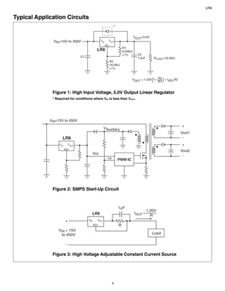
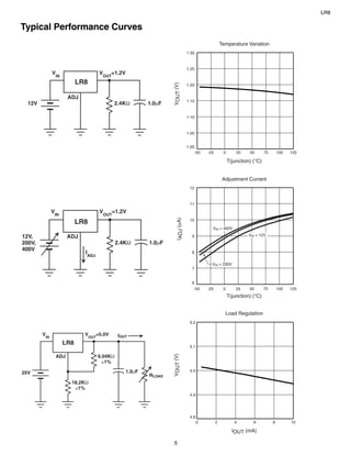
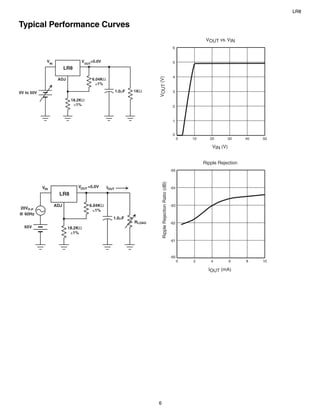
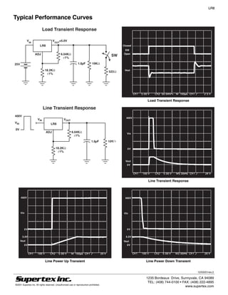

The LR8 is a high voltage, adjustable linear regulator that can regulate output voltages from 1.2V to 440V provided the input voltage is at least 10V greater than the output voltage. It has a wide input voltage range of 12V to 450V and can source output currents from 0.5mA to 10mA with 5% output voltage tolerance. The LR8 uses an external resistor divider to set the output voltage and includes current limiting, temperature limiting, and short circuit protection. It is well suited for applications requiring high input voltages such as off-line power supplies, battery chargers, and motor controls.