Download to read offline

![TPS62230, TPS62231, TPS62232, TPS62233, TPS62234
TPS62235, TPS62236, TPS62237, TPS62238, TPS62239
TPS622310, TPS622311, TPS622312, TPS622313, TPS622314
SLVS941C – APRIL 2009 – REVISED APRIL 2010 www.ti.com
These devices have limited built-in ESD protection. The leads should be shorted together or the device placed in conductive foam
during storage or handling to prevent electrostatic damage to the MOS gates.
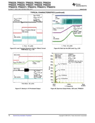
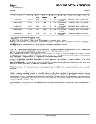
ORDERING INFORMATION
(1) FREQUENCY PACKAGE PACKAGE
TA PART NUMBER OUTPUT VOLTAGE (2) ORDERING
[MHz] DESIGNATOR MARKING
TPS62230 2.5 V 3 DRY TPS62230DRY GV
TPS62231 1.8 V 3 DRY TPS62231DRY GW
TPS62232 1.2 V 3 DRY TPS62232DRY GX
TPS62239 1.0 V 3 DRY TPS62239DRY OP
TPS622311 1.1V 2 DRY TPS622311DRY PA
TPS62235 1.2V 2 DRY TPS62235DRY OQ
TPS622313 1.3 V 3 DRY TPS62213DRY QG
TPS622314 1.5 V 3 DRY TPS622314DRY QF
–40°C to 85°C TPS62236 1.85V 2 DRY TPS62236DRY OR
TPS622312 2.0 V 3 DRY TPS622312DRY QE
TPS62234 2.1 V 3 DRY TPS62234DRY OH
TPS62238 2.25 V 3 DRY TPS62238DRY ON
TPS622310 2.3 V 3 DRY TPS622310DRY OT
(3)
TPS6223-2.7 2.7 V 3 DRY
TPS6223-2.9 (3) 2.9 V 3 DRY
TPS62233 3.0 V 3 DRY TPS62233DRY OG
TPS62237 3.3V 2 DRY TPS62237DRY OS
(1) The DRY package is available in tape on reel. Add R suffix to order quantities of 3000 parts per reel, T suffix for 250 parts per reel.
(2) Contact TI for other fixed output voltage options
(3) Device status is product preview, contact TI for more details
ABSOLUTE MAXIMUM RATINGS
(1)
over operating free-air temperature range (unless otherwise noted)
VALUE UNIT
Voltage at VIN and SW Pin (2) –0.3 to 7 V
VI Voltage at EN, MODE Pin (2) –0.3 to VIN +0.3, ≤7 V
(2)
Voltage at FB Pin –0.3 to 3.6 V
Peak output current internally limited A
HBM Human body model 2
kV
ESD rating (3) CDM Charge device model 1
Machine model 200 V
Power dissipation Internally limited
TJ Maximum operating junction temperature –40 to 125 °C
Tstg Storage temperature range –65 to 150 °C
(1) Stresses beyond those listed under absolute maximum ratings may cause permanent damage to the device. These are stress ratings
only and functional operation of the device at these or any other conditions beyond those indicated under recommended operating
conditions is not implied. Exposure to absolute–maximum–rated conditions for extended periods may affect device reliability.
(2) All voltage values are with respect to network ground terminal.
(3) The human body model is a 100-pF capacitor discharged through a 1.5-kΩ resistor into each pin. The machine model is a 200-pF
capacitor discharged directly into each pin.
2 Submit Documentation Feedback Copyright © 2009–2010, Texas Instruments Incorporated](https://image.slidesharecdn.com/tps62230-110621231637-phpapp02/85/Datasheet-of-TPS62230-2-320.jpg)
![TPS62230, TPS62231, TPS62232, TPS62233, TPS62234
TPS62235, TPS62236, TPS62237, TPS62238, TPS62239
TPS622310, TPS622311, TPS622312, TPS622313, TPS622314
www.ti.com SLVS941C – APRIL 2009 – REVISED APRIL 2010
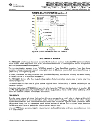
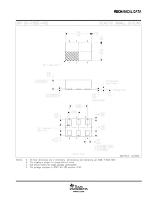
DISSIPATION RATINGS (1)
POWER RATING DERATING FACTOR
PACKAGE RqJA
FOR TA ≤ 25°C ABOVE TA = 25°C
1 × 1.5 SON 234°C/W (2) 420 mW 4.2 mW/°C
(1) Maximum power dissipation is a function of TJ(max), qJA and TA. The maximum allowable power dissipation at any allowable ambient
temperature is PD = [TJ(max) – TA] /qJA.
(2) This thermal data is measured with high-K board (4 layers board according to JESD51-7 JEDEC standard).
RECOMMENDED OPERATING CONDITIONS
operating ambient temperature TA = –40 to 85°C (unless otherwise noted) (1)
MIN NOM MAX UNIT
(2)
Supply voltage VIN 2.05 6 V
Effective inductance 2.2 mH
Effective capacitance 2.0 4.7 mF
VOUT ≤ VIN -1 V (3) 500 mA maximum IOUT (4)
3.0 3.6
Recommended minimum (5)
350mA maximum IOUT 2.5 2.7 V
supply voltage
VOUT ≤ 1.8V 60 mA maximum output current (5) 2.05
Operating virtual junction temperature range, TJ –40 125 °C
(1) In applications where high power dissipation and/or poor package thermal resistance is present, the maximum ambient temperature may
have to be derated. Maximum ambient temperature (TA(max)) is dependent on the maximum operating junction temperature (TJ(max)), the
maximum power dissipation of the device in the application (PD(max)), and the junction-to-ambient thermal resistance of the part/package
in the application (qJA), as given by the following equation: TA(max) = TJ(max) – (qJA × PD(max)).
(2) The minimum required supply voltage for startup is 2.05 V. The part is functional down to the falling UVL (Under Voltage Lockout)
threshold.
(3) For a voltage difference between minimum VIN and VOUT of ≥ 1 V
(4) Typical value applies for TA = 25°C, maximum value applies for TA = 70°C with TJ ≤ 125°C, PCB layout needs to support proper thermal
performance.
(5) Typical value applies for TA = 25°C, maximum value applies for TA = 85°C with TJ ≤ 125°C, PCB layout needs to support proper thermal
performance.
Copyright © 2009–2010, Texas Instruments Incorporated Submit Documentation Feedback 3](https://image.slidesharecdn.com/tps62230-110621231637-phpapp02/85/Datasheet-of-TPS62230-3-320.jpg)
![TPS62230, TPS62231, TPS62232, TPS62233, TPS62234
TPS62235, TPS62236, TPS62237, TPS62238, TPS62239
TPS622310, TPS622311, TPS622312, TPS622313, TPS622314
SLVS941C – APRIL 2009 – REVISED APRIL 2010 www.ti.com
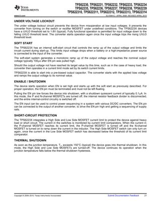
POWER SAVE MODE
Connecting the MODE pin to GND enables the automatic PWM and power-save mode operation. The converter
operates in quasi fixed frequency PWM mode at moderate to heavy loads and in the PFM (Pulse Frequency
Modulation) mode during light loads, which maintains high efficiency over a wide load current range.
In PFM Mode, the device starts to skip switch pulses and generates only single pulses with an on time of tONmin.
The PFM Mode frequency depends on the load current and the external inductor and output capacitor values.
The PFM Mode of TPS6223X is optimized for low output voltage ripple if small external components are used.
Even at low output currents, the PFM frequency is above the audible noise spectrum and makes this operation
mode suitable for audio applications.
The on time tONmin can be estimated to:
V
t ONmin = OUT ´ 260 ns
VIN (1)
Therefore, the peak inductor current in PFM mode is approximately:
(V - VOUT )
ILPFMpeak = IN ´ t ONmin
L (2)
With
tON: High side switch on time [ns]
VIN: Input voltage [V]
VOUT: Output voltage [V]
L : Inductance [mH]
ILPFMpeak : PFM inductor peak current [mA]
FORCED PWM MODE
Pulling the MODE pin high forces the converter to operate in a continuous conduction PWM mode even at light
load currents. The advantage is that the converter operates with a quasi fixed frequency that allows simple
filtering of the switching frequency for noise-sensitive applications. In this mode, the efficiency is lower compared
to the power-save mode during light loads.
For additional flexibility, it is possible to switch from power-save mode to forced PWM mode during operation.
This allows efficient power management by adjusting the operation of the converter to the specific system
requirements.
100% DUTY CYCLE LOW DROPOUT OPERATION
The device starts to enter 100% duty cycle mode once the input voltage comes close to the nominal output
voltage. In order to maintain the output voltage, the High Side switch is turned on 100% for one or more cycles.
With further decreasing VIN the High Side MOSFET switch is turned on completely. In this case the converter
offers a low input-to-output voltage difference. This is particularly useful in battery-powered applications to
achieve longest operation time by taking full advantage of the whole battery voltage range.
The minimum input voltage to maintain regulation depends on the load current and output voltage, and can be
calculated as:
VINmin = VOUT max + IOUT max ´ RDS(on)max+ RL
( ) (3)
With:
IOUTmax = maximum output current plus inductor ripple current
RDS(on)max = maximum P-channel switch RDSon.
RL = DC resistance of the inductor
VOUTmax = nominal output voltage plus maximum output voltage tolerance
20 Submit Documentation Feedback Copyright © 2009–2010, Texas Instruments Incorporated](https://image.slidesharecdn.com/tps62230-110621231637-phpapp02/85/Datasheet-of-TPS62230-20-320.jpg)
![TPS62230, TPS62231, TPS62232, TPS62233, TPS62234
TPS62235, TPS62236, TPS62237, TPS62238, TPS62239
TPS622310, TPS622311, TPS622312, TPS622313, TPS622314
www.ti.com SLVS941C – APRIL 2009 – REVISED APRIL 2010
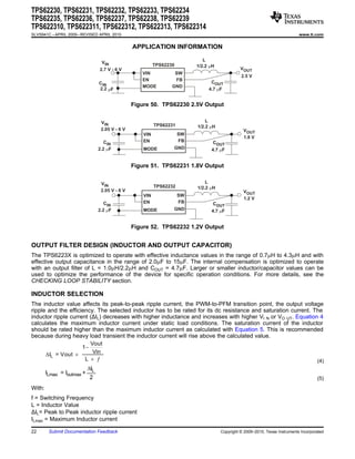
In high-frequency converter applications, the efficiency is essentially affected by the inductor AC resistance (i.e.,
quality factor) and to a smaller extent by the inductor DCR value. To achieve high efficiency operation, care
should be taken in selecting inductors featuring a quality factor above 25 at the switching frequency. Increasing
the inductor value produces lower RMS currents, but degrades transient response. For a given physical inductor
size, increased inductance usually results in an inductor with lower saturation current.
The total losses of the coil consist of both the losses in the DC resistance, R(DC), and the following
frequency-dependent components:
• The losses in the core material (magnetic hysteresis loss, especially at high switching frequencies)
• Additional losses in the conductor from the skin effect (current displacement at high frequencies)
• Magnetic field losses of the neighboring windings (proximity effect)
• Radiation losses
The following inductor series from different suppliers have been used with the TPS6223X converters.
Table 1. List of inductors
INDUCTANCE DIMENSIONS INDUCTOR TYPE SUPPLIER
[mH] [mm3]
1.0/2.2 2.5 × 2.0 × 1.2 LQM2HPN1R0MJ0 Murata
2.2 2.0 × 1.2 × 0.55 LQM21PN2R2 Murata
1.0/2.2 2.0 × 1.2 × 1.0 MIPSZ2012 FDK
1.0/2.2 2.0 × 2.5 × 1.2 MIPSA2520 FDK
1.0/2.2 2.0 × 1.2 × 1.0 KSLI2012 series Hitachi Metal
OUTPUT CAPACITOR SELECTION
The unique hysteretic PWM control scheme of the TPS62230 allows the use of tiny ceramic capacitors. Ceramic
capacitors with low ESR values have the lowest output voltage ripple and are recommended. The output
capacitor requires either an X7R or X5R dielectric. Y5V and Z5U dielectric capacitors, aside from their wide
variation in capacitance over temperature, become resistive at high frequencies.
At light load currents the converter operate in Power Save Mode and the output voltage ripple is dependent on
the output capacitor value and the PFM peak inductor current. Higher output capacitor values minimize the
voltage ripple in PFM Mode and tighten DC output accuracy in PFM Mode.
INPUT CAPACITOR SELECTION
Because of the nature of the buck converter having a pulsating input current, a low ESR input capacitor is
required for best input voltage filtering and minimizing the interference with other circuits caused by high input
voltage spikes. For most applications a 2.2mF to 4.7mF ceramic capacitor is recommended. The input capacitor
can be increased without any limit for better input voltage filtering. Because ceramic capacitor loses up to 80% of
its initial capacitance at 5V, it is recommended to use 4.7mF input capacitors for input voltages > 4.5V.
Take care when using only small ceramic input capacitors. When a ceramic capacitor is used at the input and the
power is being supplied through long wires, such as from a wall adapter, a load step at the output or VIN step on
the input can induce ringing at the VIN pin. This ringing can couple to the output and be mistaken as loop
instability or could even damage the part by exceeding the maximum ratings.
Table 2 shows a list of tested input/output capacitors.
Table 2. List of Capacitor
CAPACITANCE [mF] SIZE CAPACITOR TYPE SUPPLIER
2.2 0402 GRM155R60J225 Murata
4.7 0402 AMK105BJ475MV Taiyo Yuden
4.7 0402 GRM155R60J475 Murata
4.7 0402 CL05A475MQ5NRNC Samsung
4.7 0603 GRM188R60J475 Murata
Copyright © 2009–2010, Texas Instruments Incorporated Submit Documentation Feedback 23](https://image.slidesharecdn.com/tps62230-110621231637-phpapp02/85/Datasheet-of-TPS62230-23-320.jpg)

The TPS6223X device family is a high frequency synchronous step down DC-DC converter optimized for battery powered portable applications. It supports up to 500mA output current and allows the use of tiny and low cost chip inductors and capacitors. With a wide input voltage range of 2.05V to 6V the device supports applications powered by Li-Ion batteries with extended voltage range. The minimum input voltage of 2.05V allows as well the operation from Li-primary or two alkaline batteries. Different fixed output voltage versions are available from 1.0V to 3.3V.