This paper presents two new designs for single bit full adders using 12 transistors that reduce power consumption and output delay through varying supply voltage and utilizing reverse body bias techniques. The adder design demonstrates significant improvements in power dissipation compared to previous circuits, achieving power consumption as low as 1067.6μw and maximum output delay of 0.2316ns with reverse body bias. Simulations using TSMC 0.35μm process technology validate the performance enhancement of the proposed circuit in low-power applications.
![International Journal of Information Technology Convergence and Services (IJITCS) Vol.2, No.6, December 2012
DOI:10.5121/ijitcs.2012.2602 11
LOW POWER CMOS FULL ADDER DESIGN WITH 12
TRANSISTORS
Manoj Kumar1
, Sandeep K. Arya1
, Sujata Pandey2
1
Department of Electronics & Communication Engineering
Guru Jambheshwar University of Science & Technology, Hisar, India,
manojtaleja@yahoo.com, arya1sandeep@rediffmail.com
2
Amity University, Noida, India
spandey@amity.edu
ABSTRACT
In present work two new designs for single bit full adders have been presented using three transistors
XOR gates. Adder having twelve transistors shows power consumption of 1274µW with maximum output
delay of 0.2049ns. Power consumption and maximum output delay shows variation [1274 - 141.77] µW
& [0.2049 – 0.4167] ns with varying supply voltage from [3.3 - 1.8] V. Further, reverse body bias
technique for power reduction has been applied to adder. Adder with reverse body bias shows power
consumption variations of [1270 - 1067.60] µW with varying NMOS reverse bias from [0.0 to - 2.0] V.
Delay of adder shows variations [0.2049 - 0.2316] ns with reverse bias variation [0.0 to 2.0] V.
Simulations have been carried out at different supply voltage with increasing reverse biased applied to
NMOS transistor and results shows improvements in power consumption of adder. A comparison with
earlier reported circuits have been presented and proposed circuit’s shows less power dissipation.
KEYWORDS
CMOS, Exclusive-OR (XOR), full adder, low power design and reverse body bias.
1. INTRODUCTION
With continuous increase in complexity and number of components on integrated circuits,
power consumption of VLSI (very large scale integration) circuits is increasing at a rapid rate.
The demand and popularity of hand held battery operated devices further added research efforts
in the field of low power CMOS design. Large power consumption affects the circuit operation
and reliability by increasing temperature of circuits. Packaging and cooling costs of VLSI
system also goes up with increase in power consumptions. Three major source of power
consumption exists in CMOS circuits: 1) switching power due to output transitions 2) short
circuit power due to current between VDD and ground during switching 3) static power due to
leakage and static currents. Full adders being core building blocks in different VLSI circuits like
comparators, parity checkers, compressors. Performance of adder circuit highly affects the
overall capability of the system. Improvement in performance of full adder in terms of power
consumption, delay and other parameters will affect system capability as a whole.
Many logic styles have been used in past for designing the full adder circuits. Standard static
CMOS full adder with pull up and pull-down networks used 28 transistors [1]. Complementary
pass-transistor logic (CPL) with 32 transistors shows better driving capability but dissipates
large power [2].Transmission gate CMOS adder (TGA) was based on transmission gates and
used 20 transistors [3]. Main disadvantage of TGA was that it requires double transistors that of
pass transistor logic for implementations same logic function. A transmission function full adder
(TFA) was based on transmission function theory and used 16 transistors [4]. A full adder cell
implemented with 14 transistor using XOR design and transmission gates [5]. Multiplexer based
adder (MBA) used 12 transistors with elimination of direct path to power supply were reported
[6]. Static energy recovery full (SERF) adder with 10 transistors with reduced power](https://image.slidesharecdn.com/2612ijitcs02-241113094405-ba9a8f64/75/Low-Power-CMOS-Full-Adder-Design-with-12-Transistors-1-2048.jpg)
![International Journal of Information Technology Convergence and Services (IJITCS) Vol.2, No.6, December 2012
12
consumption at the cost of large delay had been presented [7]. Another design with 10
transistors full adder by using XOR/XNOR gates had been reported [8]. Performance analysis of
different tree structured arithmetic circuits had been presented [9]. A hybrid CMOS logic style
adder with 22 transistors had been reported [10]. A full adder using 22 transistors based on
hybrid pass logic with output drive had been presented [11]. Full adder for embedded
applications using three inputs XOR have been reported [12]. A 16 transistor full adder cell with
XOR/XNOR, pass transistors and transmission gate have been reported [13]. Structured
approach for implementation of single bit full adders using XOR/XNOR has been reported [14]
as shown in figure 1. With partitioning the full adder module into minor module, equations (1)
and equations (2) can be written as
Sum = H xor Cin = H. Cin’+ H’ Cin (1)
Cout = A. H’+ Cin. H (2)
Where H is half sum (A xor B) and H’ is complement of H.
Figure 1. Structure of single bit full adder
To reduce the standby leakage in CMOS circuits, a reverse body biasing is generally used.
Body biasing techniques make use of body terminal bias as another control mechanism to
dynamically tune threshold voltages [16]. Threshold voltage (Vth) is related by the square root
of the bias voltage implying that a significant voltage level would be needed to raise the Vth.
An optimized design is highly desirable at circuit level to avoid large power dissipation, large
delay and to achieve sufficient output level. Here, an energy efficient single bit full adders with
12 transistors using three transistor XOR gate [15], inverters and multiplexer blocks have been
presented., which shows better results in term of power dissipation. The paper is organized as
follows: In Section II, new single bit full adders using 12 transistors have been reported. In
section III results of power consumptions, maximum output delay results for the proposed full
adder’s cell have been presented and compared with earlier reported circuits. Conclusions have
been drawn in Section IV.
2. SYSTEM DESCRIPTION
New single bit adders using three transistor XOR gate [15] and multiplexer blocks are presented
in this paper. Sum and carry out (Cout) are generated by equations (1) and (2). Circuit diagram of
first proposed adder (adder-I) with two XOR gates, two inverters and two multiplexers has been
shown in figure 2. In Adder-I, Cout (carry out) signal has been generated by two transistor
multiplexer block with Cin, A and XNOR signal. Sum signal is generated with XNOR signal
generated by inverter and Cin signal. Gate lengths of all transistors have been taken as 0.35µm.
In XOR gates widths of [P1-P4] have been taken as 4.0µm whereas width of [N1-N2] has been
taken as 0.5µm. Widths of all NMOS [N3-N6] have been taken as 1.0µm whereas widths of
[P5-P7] have been taken as 2.5µm.
MODULE-I
MODULE-III
MODULE-II
Full Adder structure
Cin
B
A
H
H’
S
Cout](https://image.slidesharecdn.com/2612ijitcs02-241113094405-ba9a8f64/75/Low-Power-CMOS-Full-Adder-Design-with-12-Transistors-2-2048.jpg)
![International Journal of Information Technology Convergence and Services (IJITCS) Vol.2, No.6, December 2012
13
Figure 2. Adder-I with 12 transistors
A further improvement in above circuit has been made with reverse body bias. As CMOS
inverter is responsible for major portion of power consumption in this adder circuit. Reverse
bias voltage (V1) has been applied to two NMOS [N3 & N4] used in CMOS inverters. Substrate
terminal of PMOS [P5 & P6] transistor used in inverter are connected to VDD. By application of
reverse body bias, the Vt is increased as given in equation (3), which subsequently reduces the
sub threshold leakage currents [16], [17].
( )
f
sb
f
t
t V
V
V φ
φ
γ 2
2
0 −
+
+
= (3)
Where 0
t
V is threshold voltage for V
Vsb 0
= ; f
φ is Fermi potential and γ is substrate bias
coefficient.
Figure 3. Adder-II with reverse body bias
3. RESULTS AND DISCUSSIONS
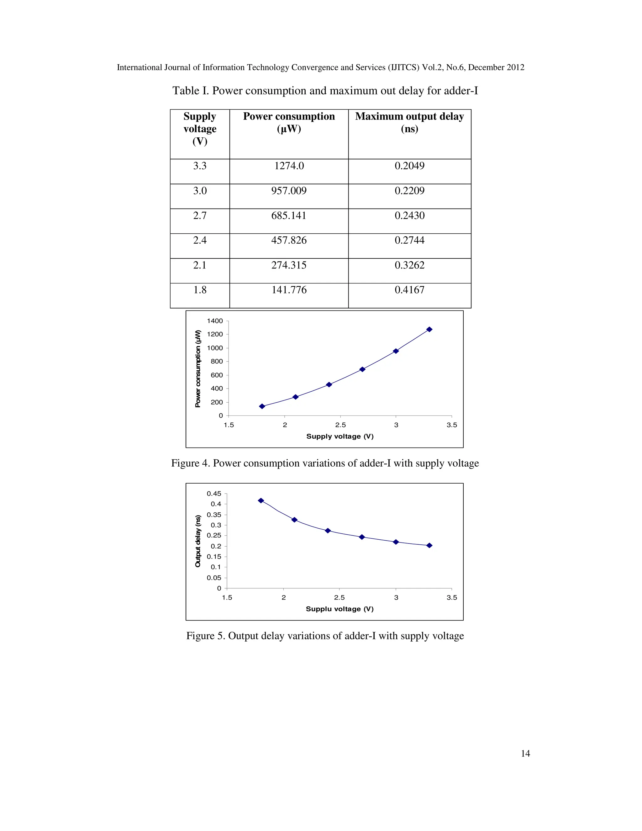
Simulations have been carried out in SPICE with TSMC 0.35µm process technology with
supply voltage of 3.3V. Table-I shows results of power consumption and maximum output
delay for adder with 12 transistors (adder-I) without reverse body bias. Supply voltage has been
varied from [3.3 - 1.8] V and power consumption and maximum output delay results have been
obtained. Figure 4 shows power consumption variation for the adder-I with varying supply
voltage. Figure 5 show effects of supply voltage on maximum out put delay. Figure 6 shows
input and output waveforms results for adder-I with supply voltage of 3.3V.
P7
P6
P5
P4 P3
P2
P1 N5
N4
N3
N2
N1
Sum
Cin
A
Cin
Cout
XOR
B
A
V1
P7
P6
P5
P4
P3
P2
P1 N5
N4
N3
N2
N1
Sum
Cin
A
Cin
Cout
XOR
B
A](https://image.slidesharecdn.com/2612ijitcs02-241113094405-ba9a8f64/75/Low-Power-CMOS-Full-Adder-Design-with-12-Transistors-3-2048.jpg)
![International Journal of Information Technology Convergence and Services (IJITCS) Vol.2, No.6, December 2012
15
Figure 6. Input and out waveforms results for adder-I
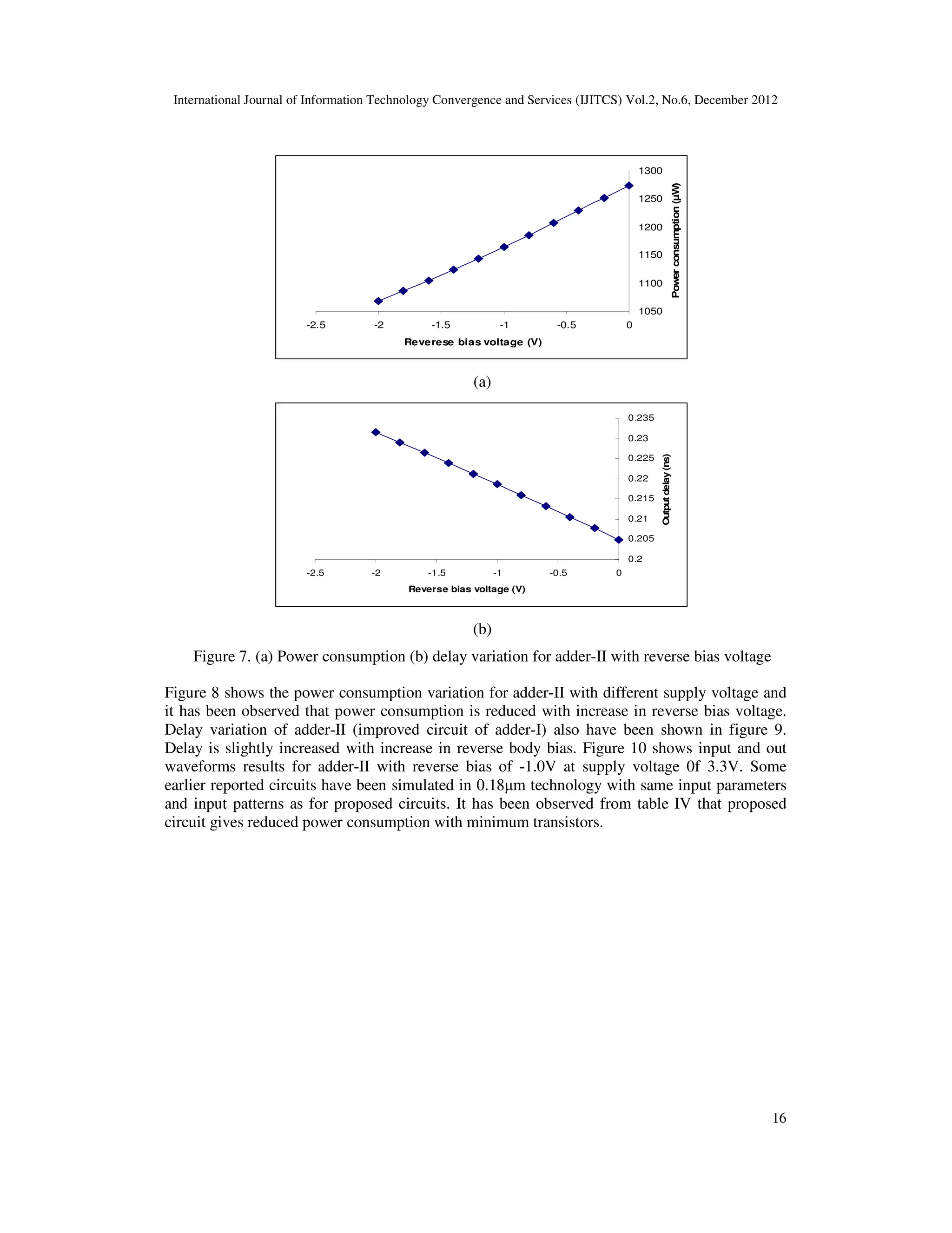
Table-II shows the power consumption and delay results for adder (adder-II) with reverse
body bias. Reverse body bias voltage has been varied from [0.0 to -2.0] V and power
consumption and delay values have been obtained. Figure 7(a) & (b) shows power
consumption and delay variation with reverse bias voltage for adder-II at 3.3V supply voltage.
Table II. Power consumption and delay with reverse bias for adder-II at 3.3 V supply
voltage
Reverse body bias voltage
(V)
Power consumption
(µW)
Maximum output delay
(ns)
0.0 1274.0 0.2049
-0.2 1252.0 0.2078
-0.4 1229.9 0.2105
-0.6 1207.9 0.2132
-0.8 1185.6 0.2159
-1.0 1164.4 0.2186
-1.2 1143.8 0.2213
-1.4 1123.9 0.2239
-1.6 1104.8 0.2265
-1.8 1086.4 0.2290
-2.0 1067.6 0.2316](https://image.slidesharecdn.com/2612ijitcs02-241113094405-ba9a8f64/75/Low-Power-CMOS-Full-Adder-Design-with-12-Transistors-5-2048.jpg)
![International Journal of Information Technology Convergence and Services (IJITCS) Vol.2, No.6, December 2012
18
0
0.05
0.1
0.15
0.2
0.25
0.3
0.35
0.4
0.45
0.5
-2.5 -2 -1.5 -1 -0.5 0
Reverse body bias (V)
Output
delay
(ns)
Vdd = 3.0V
Vdd = 2.7V
Vdd = 2.4V
Vdd = 2.1V
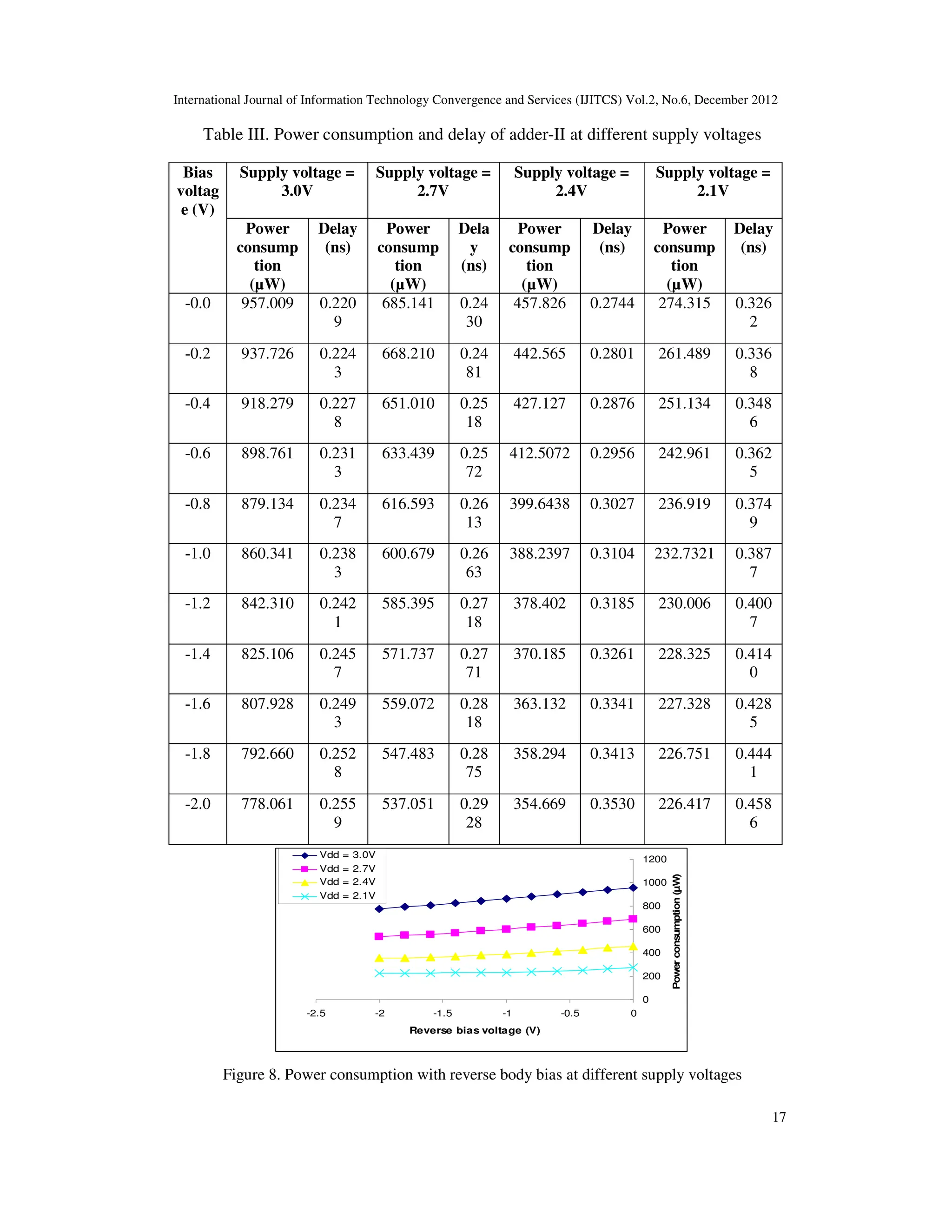
Figure 9. Output delay with reverse body bias at different supply voltages
Figure 10. Input and output waveforms for adder-II with reverse bias of -1.0Vat 3.3V supply
voltage
Table-IV. Comparison of power consumption with other circuits
Adder configuration Power consumption(µW) Number of transistors for
design
TGA20T [4] 1255.54 20
22T hybrid adder [7] 1836.4 22
22T HPSC [11] 1533.9 22
18T [3] 617.23 18
Present work adder-I 1274.0 12
Present work adder-II 1067.6 12](https://image.slidesharecdn.com/2612ijitcs02-241113094405-ba9a8f64/75/Low-Power-CMOS-Full-Adder-Design-with-12-Transistors-8-2048.jpg)
![International Journal of Information Technology Convergence and Services (IJITCS) Vol.2, No.6, December 2012
19
Power efficient adders have been designed with different combination of XOR and XNOR gates
and pass transistor multiplexer concept. Power consumption has been reduced further with
reverse body biasing of transistors. Reverse body biasing technique provides the way to reduce
power consumption without adding any extra hardware on circuit. This work gives new design
of single bit full adder with 12 transistors and extends the concept of body bias for optimized
adder design. Results show that proper selection of bias voltage reduces the power consumption
with little compromise in delay and contribute to overall performance of system.
4. CONCLUSIONS
In reported work two new circuits for single bit full adders have been reported. First circuit
designed with 12 transistors shows power consumption of 1274.0µW with delay of 0.2049 ns at
3.3V supply voltage. Adder circuit has been improved with reverse body bias technique and
gives reduced power consumption. Adder-II shows power consumption variations [1274.0 -
1067.6] µW of with varying reverse bias voltage from [0.0 to -2.0] V. Delay of adder-II shows
variation [0.2049 - 0.2316] ns with varying substrate bias from [0.0 to 2.0] V. Further, power
consumption and delay results obtained with different supply voltage shows that power
consumption has been improved in adder-II with slight increase in delay. Comparisons with
earlier reported circuits show that proposed circuits shows lesser power consumption with
reduced transistor count.
REFERENCES
[1] Y. Leblebici, S.M. Kang, CMOS Digital Integrated Circuits, Singapore: Mc Graw Hill, 2nd edition,
1999.
[2] R. Zimmermann, and W. Fichtner, “Low-power logic styles: CMOS versus pass-transistor logic,”
IEEE J. Solid State Circuits, vol. 32, no. 7, pp. 1079-1090, Jul. 1997.
[3] N. Weste and K. Eshraghian, “Principles of CMOS VLSI Design, A System Perspective,” Addison-
Wesley, 1993.
[4] N. Zhuang and H. Wu, “A new design of the CMOS full adder,” IEEE J. Solid-State Circuits, vol. 27,
no. 5, pp. 840–844, May 1992.
[5] E.Adu-Shama and M.Bayoumi, “A new cell for low power adders,” IEEE International Symposium
on Circuits and systems, vol.4, pp.49-52, May, 1996.
[6] Yingtao Jiang Al-Sheraidah, A. Yuke Wang Sha, E. and Jin-Gyun Chung, “A novel multiplexer-based
low-power full adder,” IEEE Transactions on Circuits and Systems: Express Briefs, vol. 51, no. 7,
pp.345-348, Jul. 2004.
[7] R. Shalem, E. John, and L. K. John, “A novel low-power energy recovery full adder cell,” IEEE Great
Lakes Symposium on VLSI, pp. 380 - 383, March 1999.
[8] H. T. Bui, Y. Wang, and Y. Jiang, “Design and analysis of low-power 10-transistor full adders using
XOR-XNOR gates,” IEEE Trans. Circuits Systems II, Analog Digital Signal Process, vol. 49, no. 1, pp.
25– 30, Jan. 2002.
[9] Chip-Hong Chang, Jiangmin Gu and Mingyan Zhang, “A review of 0.18µm full adder performances
for tree structured arithmetic circuits,” IEEE Transactions on Very Large Scale Integration (VLSI)
Systems, vol.13,no.6,pp.686-695, Jun.2005.
[10] S. Goel. A. Kumar, M. A. Bayoumi, “Design of robust, energy efficient full adders for deep sub
micrometer design using hybrid-CMOS logic style,” IEEE Transactions on Very Large Scale Integration
(VLSI) Systems, vol.14, no.12, pp.1309-1321, Dec. 2006.
[11] Zhang, M., J. Gu and C.H. Chang, “A novel hybrid pass logic with static CMOS output drive full-
adder cell,” IEEE International Symposium on Circuits Systems, vol. 5, pp. 317-320, May 2003.](https://image.slidesharecdn.com/2612ijitcs02-241113094405-ba9a8f64/75/Low-Power-CMOS-Full-Adder-Design-with-12-Transistors-9-2048.jpg)
![International Journal of Information Technology Convergence and Services (IJITCS) Vol.2, No.6, December 2012
20
[12] Chiou-Kou Tung, Yu-Cherng Hung, Shao-Hui Shieh, and Guo-Shing Huang, “ A Low-Power High-
Speed Hybrid CMOS Full Adder for Embedded System,” IEEE conference on Design and Diagnostics of
Electronic Circuits and Systems, pp.1-4, April, 2007.
[13] A. M. Shams and M. Bayoumi, “A novel high-performance CMOS1-bit full adder cell,” IEEE Trans.
Circuits System II, Analog Digital Signal Process, vol. 47, no. 5, pp. 478–481, May 2000.
[14] Ahmed M. Shams and Magdy A, “A structured approach for designing low power adders,” Thirty-
First Asilomar Conference on Signals, Systems & Computers, vol. 1, pp.757-761, Nov. 1997.
[15] Manoj Kumar, Sandeep K. Arya and Sujata Pandey,” A new low power single bit full adder design
with 14 transistors using novel 3 transistors XOR gate,” IEEE international conference on computer
modeling and simulation, vol.2, pp. 222-226,Jan.7-9, 2011.
[16] Keivan Navi, Omid Kavehie, Mahnoush Rouholamini, Amir Sahafi, and Shima Mehrabi, “A novel
CMOS full adder,” IEEE International Conference on VLSI Design, pp. 303-307, Jan. 2007.
[17] Dong Whee Kim, Jeong Beom Kim, “Low-power carry look-ahead adder with multi-threshold
voltage CMOS technology,” International Semiconductor Conference (CAS), vol.2, pp. 537-540, Sept.
2008.
[19] Keivan navi and Omid Kavehei, “Low-power and high-performance 1-bit CMOS full-adder cell,”
Journal of Computers, vol. 3, no. 2, pp. 48-54, Feb. 2008.
[20] Nima Taherinejad and Adib Abrishamifar, “A new high speed, low power adder; using hybrid
analog-digital circuits,” European Conference on circuit Theory and Design (ECCTD), pp. 623-626, Aug.
2009.
[21] Shiv Shankar Mishra, S. Wairya, R.K. Nagaria and S. Tiwari, “New design methodologies for high
speed low power XOR-XNOR circuits,” World Academy of Science, Engineering and Technology,
vol.55, pp. 200-206, 2009.
[22] M.Hosseinghadiry, H. Mohammadi, M. Nadisenejani, “Two new low power high performance full
adders with minimum gates,” World Academy of Science, Engineering and Technology, vol. 52, pp. 1077-
1084, 2009.
[23] Farshad Moradi, Dag.T. Wisland, Hamid Mahmoodi,Snorre Aunet,Tuan Vu Cao, Ali Peiravi, “Ultra
low power full adder topologies,” IEEE International Symposium on Circuits and Systems, pp. 3158 –
3161, May 2009.
[24] Dan Wang, Maofeng Yang, Wu Cheng, Xuguang Guan, Zhangming Zhu, Yintang Yang, “Novel low
power full adder cells in 180nm CMOS technology,” IEEE Conference on Industrial Electronics and
Applications (ICIEA), pp. 430-433, May 2009.
[25] Chuen-Yau Chen and Yung-Pei Chou, “Novel low-power 1-bit full adder design,” International
Symposium on Communications and Information Technology, pp. 1348-1349, Sept. 2009.
[26] Reza Faghih Mirzaee, Mohammad Hossein Moaiyeri, Keivan Navi, “High speed np-CMOS and
multi-output dynamic full adder cells,” International Journal of Electrical and Electronics Engineering,
vol. 4, pp. 304-310, 2010
[16] Adel S. Sedra and K. C. Smith, Microelectronics circuits, Oxford University press, New York, 1998.
[17] Kaushik Roy, Sharat C. Prasad, Low power CMOS circuit design, India: Wiely Pvt Ltd, Feb. 2002.
Authors
Dr. Manoj Kumar is working as assistant professor in Electronics & Communication Engineering, Guru
Jambheshwar University of Science & Technology, Hisar, INDIA. He has published more than 15
research papers in international/national journals. His research interests include low power CMOS
system, Integrated circuit designs and microelectronics. He is a Life Member of IETE (India), ISTE
(India) and member of Semiconductor Society of India.](https://image.slidesharecdn.com/2612ijitcs02-241113094405-ba9a8f64/75/Low-Power-CMOS-Full-Adder-Design-with-12-Transistors-10-2048.jpg)