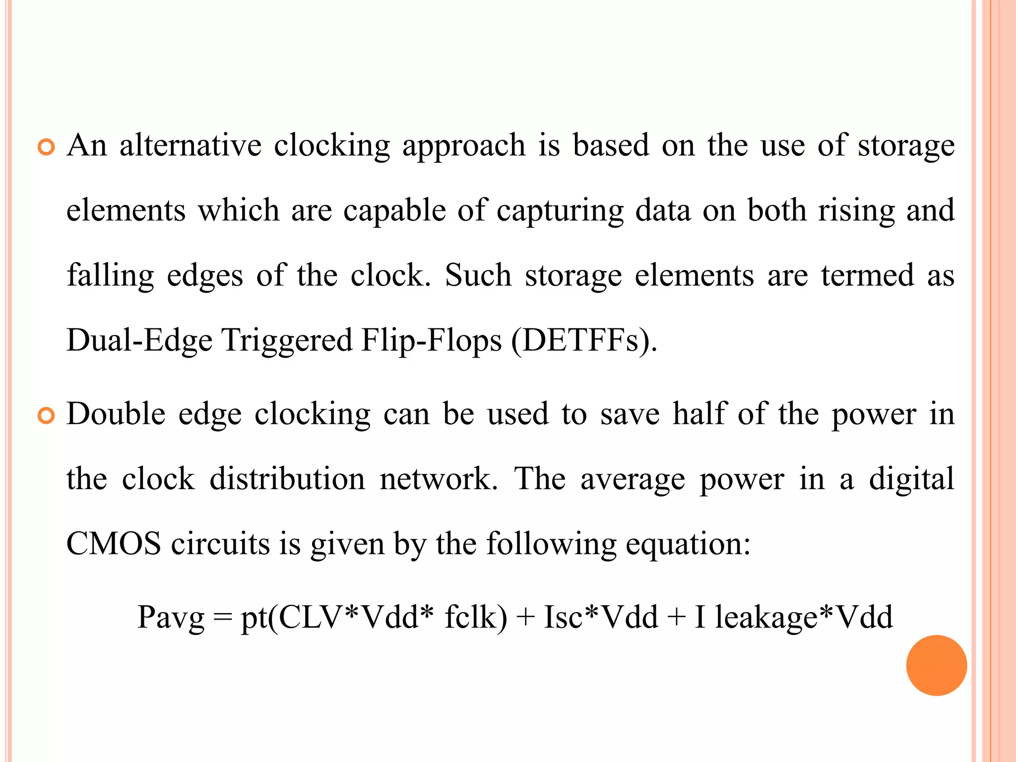
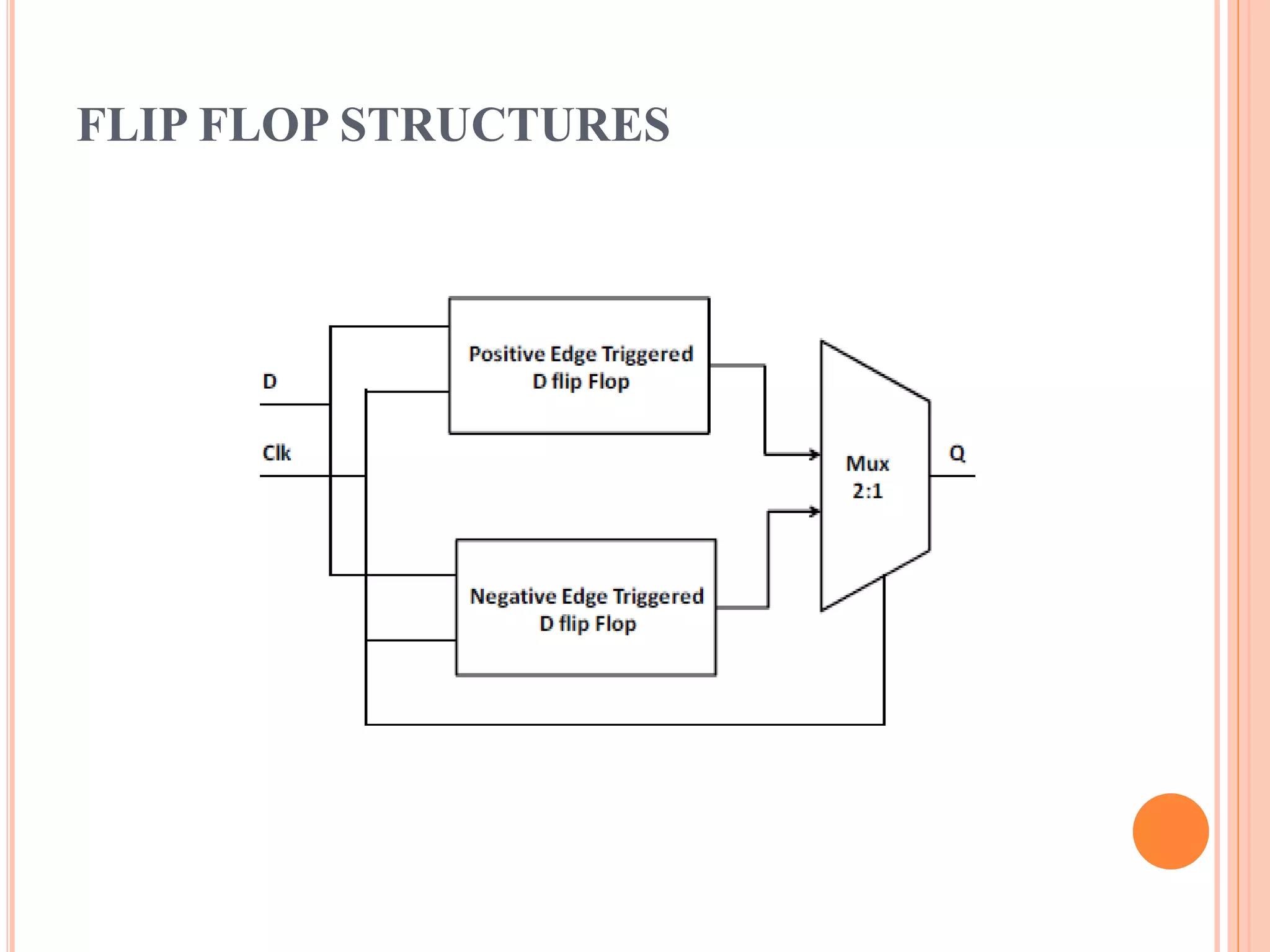
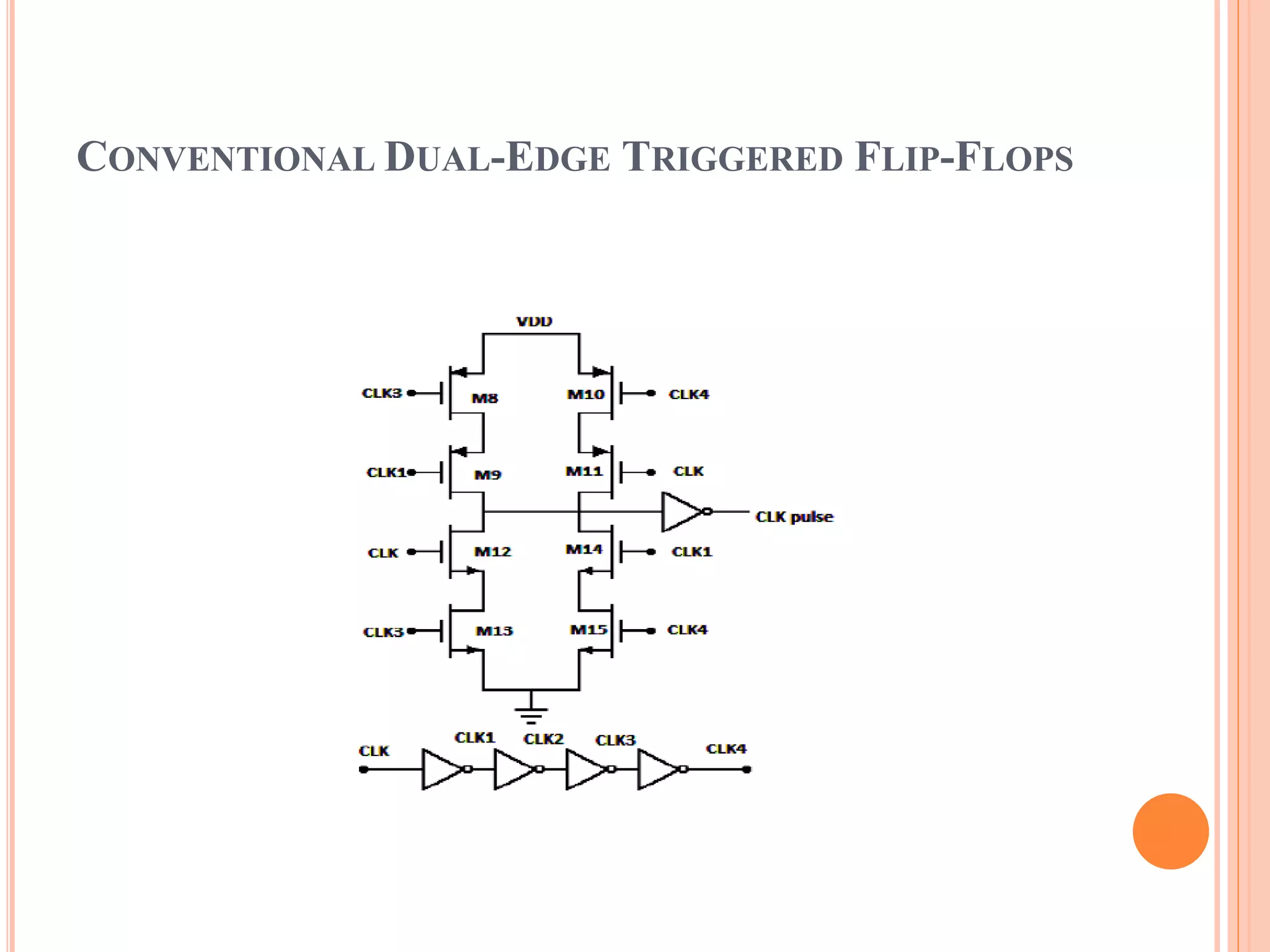
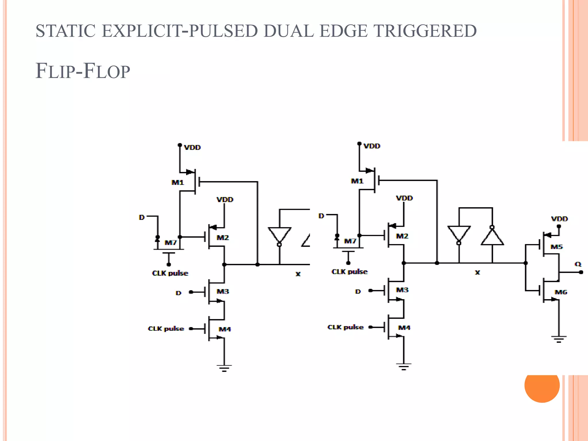
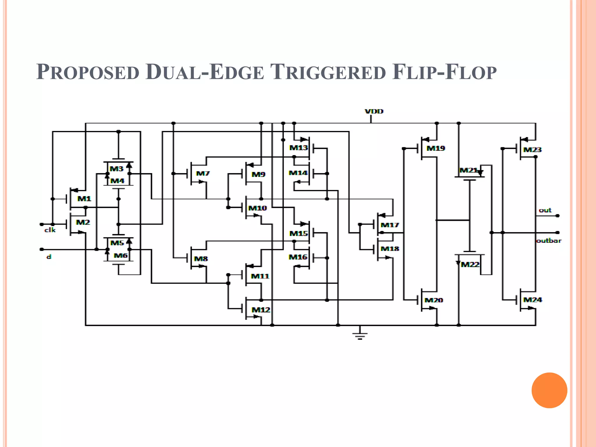
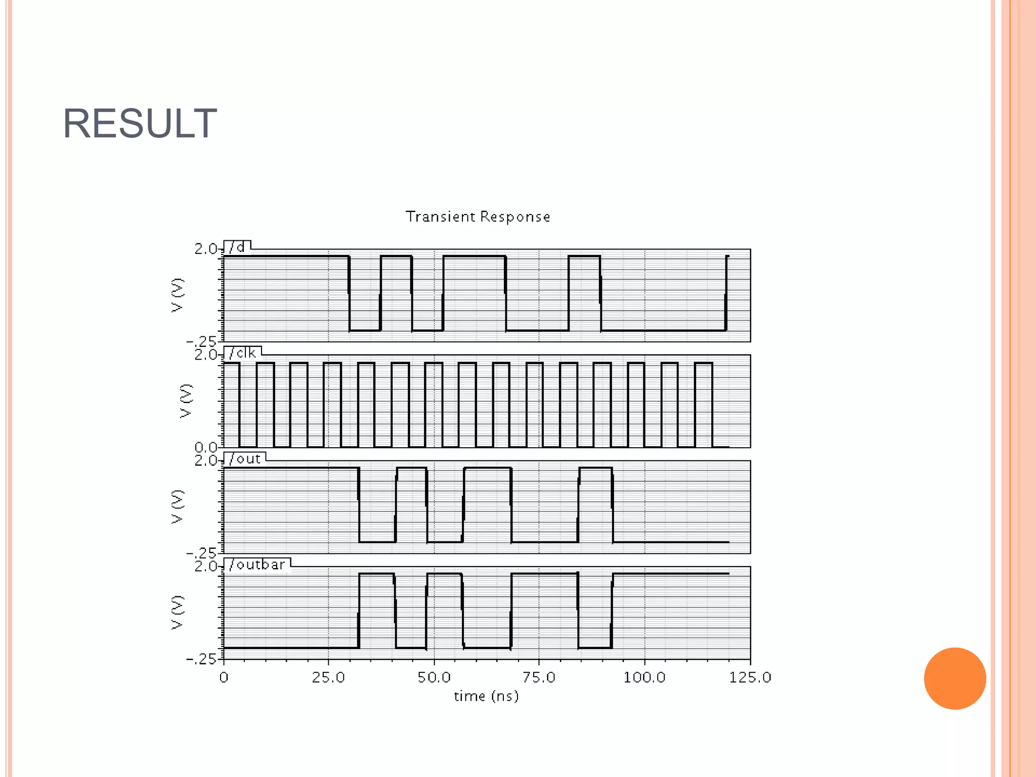
LOW POWER DUAL EDGE -
TRIGGERED STATIC D FLIP-FLOP
By
B.Nagajyothi
 Flip-Flop have a great impact on circuit power
consumption and speed.
 improving the performance one innovating approach is to
increase the clock frequency.
 using high clock frequency Power consumption of the
clock system increases.
 An alternative clocking approach is based on the use of storage
elements which are capable of capturing data on both rising and
falling edges of the clock. Such storage elements are termed as
Dual-Edge Triggered Flip-Flops (DETFFs).
 Double edge clocking can be used to save half of the power in
the clock distribution network. The average power in a digital
CMOS circuits is given by the following equation:
Pavg = pt(CLV*Vdd* fclk) + Isc*Vdd + I leakage*Vdd
FLIP FLOP STRUCTURES
 DETFF approach is preferred to reduce power
dissipation Unlike SETFF, data is captured by both edges
of the clock.
 Both positive and negative edges are used to sample the
D input at alternate clock edges, and the appropriate
sample is selected for the Q output by a clocked
multiplexer (MUX).
CONVENTIONAL DUAL-EDGE TRIGGERED FLIP-FLOPS
STATIC EXPLICIT-PULSED DUAL EDGE TRIGGERED
FLIP-FLOP
PROPOSED DUAL-EDGE TRIGGERED FLIP-FLOP
 In the proposed DETFF, positive latch and negative latch are
connected in parallel.
 These latches are designed using one transmission gate and two
inverters connected back to back and the output of both the
latches are connected to 2:1Mux as input.
 Mux is designed using one PMOS and one NMOS connected in
series and gates are connected together and derived by the
inverted CLK. Output of Mux is connected to the inverter for
strengthening the output.
 Back to back connected inverters hold the data when
transmission gate is OFF and at the same time Mux sends the
latched data to the inverter to get the correct D at the output.
 The proposed DETFF works as follows. When the CLK is low
M3, M4 and M18 are ON and M5,M6 and M17 are OFF. Hence
data hold by negative latch is transparent to Q. When CLK is
high.
 The proposed DETFF works as follows. When the CLK is low
M3, M4 and M18 are ON and M5,M6 and M17 are OFF. Hence
data hold by negative latch is transparent to Q.
 When CLK is high M5, M6 and M17 are ON and M3,
M4 and M18 are OFF. If input D remains the same, Q
also remains unchanged.
 On the other hand, if D is changed before the CLK then
D will be hold by positive latch and the same value will
be send to the output when CLK changes from Low to
high and similarly for the transition of CLK from high to
low.
RESULT

LOW POWER DUAL EDGE - TRIGGERED STATIC D FLIP-FLOP

  • 1.
    LOW POWER DUALEDGE - TRIGGERED STATIC D FLIP-FLOP By B.Nagajyothi
  • 2.
     Flip-Flop havea great impact on circuit power consumption and speed.  improving the performance one innovating approach is to increase the clock frequency.  using high clock frequency Power consumption of the clock system increases.
  • 3.
     An alternativeclocking approach is based on the use of storage elements which are capable of capturing data on both rising and falling edges of the clock. Such storage elements are termed as Dual-Edge Triggered Flip-Flops (DETFFs).  Double edge clocking can be used to save half of the power in the clock distribution network. The average power in a digital CMOS circuits is given by the following equation: Pavg = pt(CLV*Vdd* fclk) + Isc*Vdd + I leakage*Vdd
  • 4.
  • 5.
     DETFF approachis preferred to reduce power dissipation Unlike SETFF, data is captured by both edges of the clock.  Both positive and negative edges are used to sample the D input at alternate clock edges, and the appropriate sample is selected for the Q output by a clocked multiplexer (MUX).
  • 6.
  • 7.
    STATIC EXPLICIT-PULSED DUALEDGE TRIGGERED FLIP-FLOP
  • 8.
  • 9.
     In theproposed DETFF, positive latch and negative latch are connected in parallel.  These latches are designed using one transmission gate and two inverters connected back to back and the output of both the latches are connected to 2:1Mux as input.  Mux is designed using one PMOS and one NMOS connected in series and gates are connected together and derived by the inverted CLK. Output of Mux is connected to the inverter for strengthening the output.
  • 10.
     Back toback connected inverters hold the data when transmission gate is OFF and at the same time Mux sends the latched data to the inverter to get the correct D at the output.  The proposed DETFF works as follows. When the CLK is low M3, M4 and M18 are ON and M5,M6 and M17 are OFF. Hence data hold by negative latch is transparent to Q. When CLK is high.  The proposed DETFF works as follows. When the CLK is low M3, M4 and M18 are ON and M5,M6 and M17 are OFF. Hence data hold by negative latch is transparent to Q.
  • 11.
     When CLKis high M5, M6 and M17 are ON and M3, M4 and M18 are OFF. If input D remains the same, Q also remains unchanged.  On the other hand, if D is changed before the CLK then D will be hold by positive latch and the same value will be send to the output when CLK changes from Low to high and similarly for the transition of CLK from high to low.
  • 12.