Downloaded 141 times
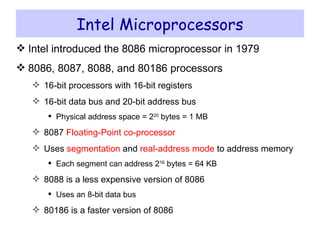
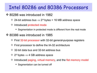
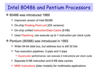
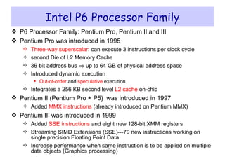

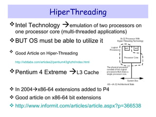
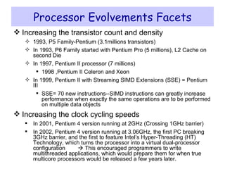


The document provides an overview of the evolution of Intel microprocessors from 8-bit to 64-bit architectures over several decades. It describes key processors such as the 8086, 80286, 80386 which introduced 32-bit architecture and protected mode. Subsequent processors increased performance through features like pipelining, superscalar, and integration of memory controllers and caches on-die. Modern multi-core processors support 64-bit architecture and virtualization.