This paper presents the design and implementation of an Advanced Modified Booth Encoding (AMBE) multiplier capable of performing multiplication for both signed and unsigned 32-bit numbers, addressing the limitations of existing multipliers which typically handle only signed or unsigned operations. The proposed design uses a modified booth algorithm to generate partial products efficiently and incorporates carry save adders and carry look-ahead adders to enhance speed and reduce power consumption. The result is a high-speed multiplier architecture that minimizes chip area and power dissipation while maintaining a high performance suitable for modern computing systems.
![International Journal of Engineering Science Invention
ISSN (Online): 2319 – 6734, ISSN (Print): 2319 – 6726
www.ijesi.org Volume 2 Issue 8 ǁ August. 2013 ǁ PP.60-68
www.ijesi.org 60 | Page
Design and Implementation of Advanced Modified Booth
Encoding Multiplier
Shaik.Kalisha Baba1
, D.Rajaramesh2
1,2, (ECE, Mvgr College Of Engineering, India)
ABSTRACT:- This paper presents the design and implementation of Advanced Modified Booth Encoding
(AMBE) multiplier for both signed and unsigned 32 - bit numbers multiplication. The already existed Modified
Booth Encoding multiplier and the Baugh-Wooley multiplier perform multiplication operation on signed
numbers only. Where as the array multiplier and Braun array multipliers perform multiplication operation on
unsigned numbers only. Thus, the requirement of the modern computer system is a dedicated and very high
speed unique multiplier unit for signed and unsigned numbers. Therefore, this paper presents the design and
implementation of AMBE multiplier. The modified Booth Encoder circuit generates half the partial products in
parallel. By extending sign bit of the operands and generating an additional partial product the AMBE
multiplier is obtained. The Carry Save Adder (CSA) tree and the final Carry Look ahead (CLA) adder used to
speed up the multiplier operation. Since signed and unsigned multiplication operation is performed by the same
multiplier unit the required hardware and the chip area reduces and this in turn reduces power dissipation and
cost of a system.
KEY WORDS: Modified Booth Encoding multiplier, CSA,CLA, Signed-unsigned.
I. INTRODUCTION
Multiplication is a most commonly used operation in many computing systems. Infact multiplication is
nothing but addition since, multiplicand adds to itself multiplier no.of times gives the multiplication value
between multiplier and multiplicand. But considering the fact that this kind of implementation really takes huge
hardware resources and the circuit operates at utterly low speed. In order to address this so many ideas have
been presented so far for the last three decades. Each one is aimed at particular improvement according to the
requirement. One may be aimed at high clock speeds and another mayb e aimed for low power or less area
occupation. Either way ultimate job is to come up with an efficient architecture which can address three
constraints of VLSI speed, area, and power. Among these three speed is the one which requires special attention.
If we observe closely multiplication operation involves two steps one is producing partial products and adding
these partial products [3]. Thus, the speed of a multiplier hardly depends on how fast generate the partial
products and how fast we can add them together. If the number of partial products to be generated are of less
then it is indirectly means that we have achieved the speed in generating partial products. Booth’s algorithms are
meant for this only. To speed up the addition among the partial products we need fast adder architectures.
Since the multipliers have a significant impact on the performance of the entire system, many high performance
algorithms and architectures have been proposed [1-12]. The very high speed and dedicated multipliers are used
in pipeline and vector computers.
The high speed Booth multipliers and pipelined Booth multipliers are used for digital signal processing
(DSP) applications such as for multimedia and communication systems. High speed DSP computation
applications such as Fast Fourier transform (FFT) require additions and multiplications. The conventional
modified Booth encoding (MBE) generates an irregular partial product array because of the extra partial product
bit at the least significant bit position of each partial product row. Therefore papers [4] presents a simple
approach to generate a regular partial product array with fewer partial product rows and negligible overhead,
there by lowering the complexity of partial product reduction and reducing the area, delay, and power of MBE
multipliers. But the drawback of this multiplier is that it function only for signed number operands.
The modified-Booth algorithm is extensively used for high-speed multiplier circuits. Once, when array
multipliers were used, the reduced number of generated partial products significantly improved multiplier
performance. In designs based on reduction trees with logarithmic logic depth, however, the reduced number of
partial products has a limited impact on overall performance. The Baugh-Wooley algorithm [7,8,9] is a different
scheme for signed multiplication, but is not so widely adopted because it may be complicated to deploy on](https://image.slidesharecdn.com/j0281060068-130926021134-phpapp01/85/International-Journal-of-Engineering-and-Science-Invention-IJESI-1-320.jpg)
![Design And Implementation Of…
www.ijesi.org 61 | Page
irregular reduction trees. Again the Baugh-Wooley algorithm is for only signed number multiplication. The
array multipliers and Braun array multipliers [10] operates only on the unsigned numbers. Thus, the requirement
of the modern computer system is a dedicated and very high speed multiplier unit that can perform
multiplication operation on signed as well as unsigned numbers. In this paper we designed and implemented a
dedicated multiplier unit that can perform multiplication operation on both signed and unsigned numbers, and
this multiplier is called as AMBE multiplier.
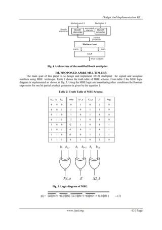
II. CONVENTIONAL MODIFIED BOOTH MULTIPLIER
2.1. Algorithm of the Modified Booth Multiplier :-
Multiplication consists of three steps: 1) the first step to generate the partial products; 2) the second
step to add the generated partial products until the last two rows are remained; 3) the third step to compute the
final multiplication results by adding the last two rows. The modified Booth algorithm reduces the number of
partial products by half in the first step. We used the modified Booth encoding (MBE) scheme proposed in [2].
It is known as the most efficient Booth encoding and decoding scheme. To multiply X by Y using the modified
Booth algorithm starts from grouping Y by three bits and encoding into one of {-2, -1, 0, 1, 2}. Table I shows
the rules to generate the encoded signals by MBE scheme and Fig. 1 (a) shows the corresponding logic diagram.
The Booth decoder generates the partial products using the encoded signals as shown in Fig. 1(b).
Table 1: TRUTH TABLE OF MBE SCHEME.
Fig. 1. The Encoder and Decoder for the new MBE scheme.
(a) Simple encoder (b) Decoder.
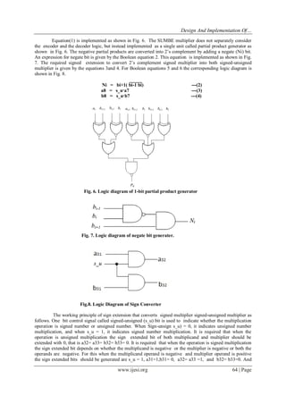
The new MBE recorder [2] was designed according to the following analysis. Table (1) presents the
truth table of the new encoding scheme. The Z signal makes the output zero to compensate the incorrect X2_b
and Neg signals. Fig. 1 presents the circuit diagram of the encoder and decoder. The encoder generates X1_b,](https://image.slidesharecdn.com/j0281060068-130926021134-phpapp01/85/International-Journal-of-Engineering-and-Science-Invention-IJESI-2-320.jpg)
![Design And Implementation Of…
www.ijesi.org 62 | Page
X2_b, and Z signals by encoding the three x-signals. The y LSB signal is the LSB of the y signal and is
combined with x-signals to determine the Row_LSB and the Neg_cin signals. Similarly, yMSB is combined
with x- signals to determine the sign extension signals.
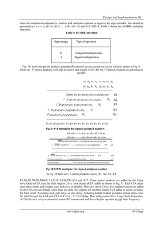
Fig. 2. 8× 8 MBE partial product array. (a) Traditional MBE partialproduct
array. (b) New MBE partial product array.
The Fig. 2(a) has widely been adopted in parallel multipliers since it can reduce the number of partial
product rows to be added by half, thus reducing the size and enhancing the speed of the reduction tree.
However, as shown in Fig. 1(a), the conventional MBE algorithm generates n/2 + 1 partial product rows rather
than n/2 due to the extra partial product bit (neg bit) at the least significant bit position of each partial product
row for negative encoding, leading to an irregular partial product array and a complex reduction tree. Therefore,
the Modified Booth multipliers with a regular partial product array [4] produce a very regular partial product
array, as shown in Fig. 3. Not only each negi is shifted left and replaced by ci but also the last neg bit is
removed. This approach reduces the partial product rows from n/2 + 1 to n/2 by incorporating the last neg bit
into the sign extension bits of the first partial product row, and almost no overhead is introduced to the partial
product generator. More regular partial product array and fewer partial product rows result in a small and fast
reduction tree, so that the area, delay, and power of MBE multipliers can further be reduced.
Fig. 3 Generated partial products and sign extension scheme
Fig. 3 shows the generated partial products and sign extension scheme of the 8-bit modified
Booth multiplier. The partial products generated by the modified Booth algorithm are added in parallel using
the Wallace tree until the last two rows are remained. The final multiplication results are generated by
adding the last two rows. The carry propagation adder is usually used in this step.
2.2. Architecture of the Modified Booth Multiplier :-
Fig. 4 shows the architecture of the commonly used modified Booth multiplier. The inputs of the
multiplier are multiplicand X and multiplier Y. The Booth encoder encodes input Y and derives the
encoded signals as shown in Fig. 1 (a). The Booth decoder generates the partial products according to the
logic diagram in Fig. 1 (b) using the encoded signals and the other input X. The Wallace tree computes the
last two rows by adding the generated partial products. The last two rows are added to generate the final
multiplication results using the carry look-ahead adder (CLA).](https://image.slidesharecdn.com/j0281060068-130926021134-phpapp01/85/International-Journal-of-Engineering-and-Science-Invention-IJESI-3-320.jpg)
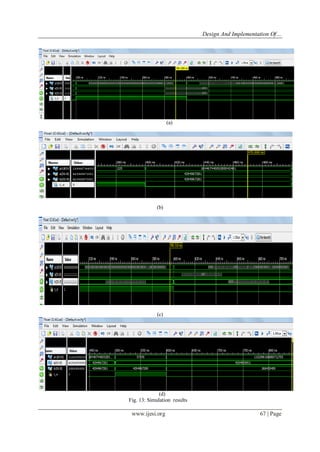
![Design And Implementation Of…
www.ijesi.org 68 | Page
V. CONCLUSION
In this paper, we present a 32-bit×32-bit advanced multiplier capable of carrying out both signed and
unsigned operations. The proposed novel unified signed/unsigned multiplier was optimized in terms of speed,
power consumption and silicon area by exploiting more regular partial product array, developing more efficient
compression methods and combining several types of fast adders
REFERENCES
[1] W. –C. Yeh and C. –W. Jen, “High Speed Booth encoded Parallel Multiplier Design,” IEEE transactions on computers, vol. 49,
no. 7, pp. 692-701, July 2000.
[2] Shiann-Rong Kuang, Jiun-Ping Wang, and Cang-Yuan Guo, “Modified Booth multipliers with a Regular Partial Product Array,”
IEEE Transactions on circuits and systems-II, vol 56, No 5, May 2009.
[3] Li-Rong Wang, Shyh-Jye Jou and Chung-Len Lee, “A well-tructured Modified Booth Multiplier Design” 978-1-4244-1617-
2/08/$25.00 ©2008 IEEE.
[4] Soojin Kim and Kyeongsoon Cho “Design of High-speed Modified Booth Multipliers Operating at GHz Ranges” World
Academy of Science, Engineering and Technology 61 2010.
[5] Magnus Sjalander and Per Larson-Edefors. “The Case for HPM-Based Baugh-Wooley Multipliers,” Chalmers University of
Technology, Sweden, March 2008
[6] J. Fadavi-Ardekani, ªM×N Booth Encoded Multiplier Generator Using Optimized Wallace Trees,º IEEE Trans. VLSI Systems,
vol. 1,no. 2, June 1993.
[7] Wang, G., “A unified unsigned/signed binary multiplier”, TheThirty-Eighth Asilomar Conference on Signals, Systems
andComputers, 2004, Vol. 1, pp.:513 - 516, Nov 7-10, 2004.
[8] Kim J. Y., “Multiplier to selectively perform unsigned magnitude multiplication or signed magnitude multiplication”,USpatent
5,870,322, Feb 9, 1999.
[9] Hwang-Cherng Chow and I-Chyn Wey, “A 3.3V 1GHz high speed pipelined Booth multiplier,” Proc. of IEEE ISCAS, vol.
1, pp. 457-460, May 2002.
[10] M. Aguirre-Hernandez and M. Linarse-Aranda, “Energy-efficient high-speed CMOS pipelined multiplier,” Proc. of IEEE
CCE, pp. 460-464, Nov. 2008.
[11] A. D. Booth, “A signed binary multiplication technique,” Quarterly J. Mechanical and Applied Math, vol. 4, pp.236-240,
1951.
[12] Kuang S. R., Wang J. P., Guo C. Y., “Modified Booth Multipliers With a Regular Partial Product Array”,IEEETransactions on
Circuits and Systems II: Express Briefs,Vol.56, Issue 5, pp.:404 - 408, May, 2009.
[13] Jung-Yup Kang and Jean-Luc Gaudiot, “A simple high-speed multiplier design,” IEEE Trans. on Computers, vol. 55, issue
10, Oct. pp. 1253-1258, 2006.](https://image.slidesharecdn.com/j0281060068-130926021134-phpapp01/85/International-Journal-of-Engineering-and-Science-Invention-IJESI-9-320.jpg)