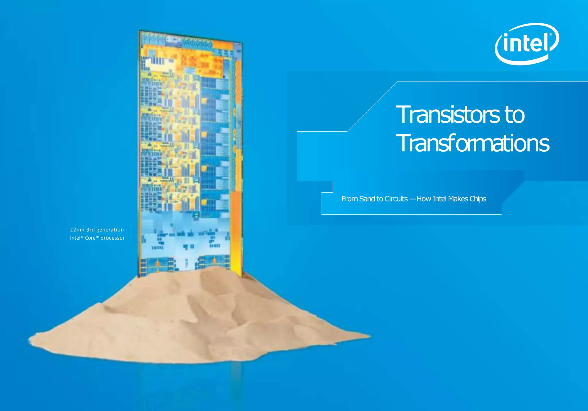
The document discusses Intel's development of 22nm 3rd generation Core processors using 3-D Tri-Gate transistors. It summarizes Moore's Law of transistors doubling every couple years, and how Intel innovations like strained silicon and high-k/metal gate technologies have allowed continued advancement. The document outlines Intel's advanced chip design and manufacturing processes, from obtaining pure silicon to photolithography patterning on wafers to produce chips with billions of transistors.
An Introduction to Semiconductors and IntelDESMOND YUEN
Did you know that...
The average American adult spends over 12 hours a day engaged with electronics — computers, mobile devices, TVs, cars, to name just a few — powered by semiconductors.
A common chip the size of your smallest fingernail is only about 1-millimeter thick but contains roughly 30 different layers of components and wires (called interconnects) that make up its complex circuitry.
Intel owns nearly 70,000 active patents worldwide. Its first — “Resistor for Integrated Circuit,” #3,631,313 — was granted to Gordon Moore on Dec. 28, 1971.
Those are a few fun facts in a high-level presentation that provides an easy-to-understand look at the world of semiconductors, why they matter and the role Intel plays in their creation.
Very-large-scale integration (VLSI) is the process of creating an integrated circuit (IC) by combining thousands of transistors into a single chip. VLSI began in the 1970s when complex semiconductor and communication technologies were being developed. The microprocessor is a VLSI device.
Before the introduction of VLSI technology, most ICs had a limited set of functions they could perform. An electronic circuit might consist of a CPU, ROM, RAM and other glue logic. VLSI lets IC designers add all of these into one chip.
The electronics industry has achieved a phenomenal growth over the last few decades, mainly due to the rapid advances in large scale integration technologies and system design applications. With the advent of very large scale integration (VLSI) designs, the number of applications of integrated circuits (ICs) in high-performance computing, controls, telecommunications, image and video processing, and consumer electronics has been rising at a very fast pace.
The current cutting-edge technologies such as high resolution and low bit-rate video and cellular communications provide the end-users a marvelous amount of applications, processing power and portability. This trend is expected to grow rapidly, with very important implications on VLSI design and systems design.
Applications of various latest coprocessorsSejal Anand
A coprocessor is a chip that works side-by-side with the computer's main processor (the chip called the central processing unit, or CPU).
Math processor can perform high-level mathematical operations such as logarithms, roots, trigonometry functions much faster than the main processor. It also performs floating point math. The instruction set of the math processor is different from the instruction set of the main processor.
Network processor handles incoming and outgoing network traffic in high-end systems. It is optimized to process a large number of incoming and outgoing network packets.
Crypto-processor is a special processor that supports cryptography. It performs message encryption and decryption for secure data transmission.
Graphics Processing Unit handles high-resolution graphics processing. It consists of multiple cores with small instruction sets.
Given on Back to the Future Day, this presentation showcased the latest and greatest new tech gadgets, discoveries, and inventions for addressing quality of life and societal issues, as well as others for business effectiveness, personal productivity, and just plain fun. It shares a forward-looking view of emerging tech innovations illuminating what they portent for individuals, projecting evolving market opportunities, and gauging the impact on society at large from the present on into our future. Contemporary science fiction and that of the past often influences and anticipates the technological advances we see today and what we hope and fear for tomorrow. View and/or download this rollicking ride through the technology roller coaster of our times.
See latest version (10/21/15) at http://www.slideshare.net/markgirc/wfs-az-todays-gadgets-emerging-technology-innovations-102115 (or http://bit.ly/1GrghpU) given to the World Future Society Arizona on Back to the Future Day.
Today’s Gadgets & Emerging Technology Innovations 4/1/15:
In a presentation to the IEEE Computer Society Phoenix, Mark Goldstein, International Research Center (http://www.researchedge.com/) showcased the latest and greatest new tech gadgets for business effectiveness, personal productivity, improving quality of living, and just plain fun. He shared a forward-looking view of emerging technology innovations and analysis of what they portent for information technology professionals, evolving market opportunities, and society at large from the present on into our future. Contemporary science fiction and that of the past often influences and anticipates the technological advances we see today and what we hope and fear for tomorrow. View/download and share a rollicking ride through the technology roller coaster of our times.
Internet of Things Connectivity for Embedded Devicesmentoresd
Slides presented at "Internet of Things Connectivity for Embedded Devices" live event by Mentor Graphics Embedded Software and Nano Power Communication. See the live event here: https://plus.google.com/u/0/events/cfgduqagg4r5l871uogca4ujea0
Please contact embedded_software@mentor.com for any questions or inquiries.
System-On-Chip Market Outlook, Trends, Forecast of Top Countries 2023Adhiraj Kumar
The system on chip is a type of integrated circuit which synchronize all the component of the computer peripherals and electronics devices. The system on chip is composed of microprocessor, microcontroller, memory blocks, timing sources and many power integrated circuits.
Get Complete Report @ https://www.marketresearchfuture.com/reports/system-on-chip-market-2207
it is all about the generation of computer. explained in a detailed way. helpful for those students who is seeking information about computer generation.it is available in one place
A Dell lança uma peça chave para projetos IoT: o “Edge Gateway”. Vamos apresentá-lo pessoalmente, mencionaremos os demais elementos que a Dell oferece na área e lembraremos todos os elementos, próprios e de terceiros, que devem compor um projeto IoT. Também discutiremos os fatores críticos de sucesso e mostraremos como um projeto IoT pode ser iniciado, com sucesso, hoje mesmo!
Global Technology Trends - Electronic SystemsIan Phillips
The practical application of a couple of centuries of scientific study has brought huge advances to almost everything we value; but none more so than those touched by Electronic Systems whose power to transform and animate is truly phenomenal. Surely with such powerful magic, anything is within our power: Mend climates, solve energy problems and cure society's ills?! Alas not; our tricks are not magic, but the results of painstaking global enterprise, of immense scale, detail and precision. And whilst our technologies are evolving at a prodigious rate; they are only capable of achieving so-much at any given time. The consumers insatiable appetite spurs us endlessly on. Perceive the reality of Electronic Systems and we can cauterise our vulnerabilities, whilst capitalising the many and varied business and economic opportunities they present as they deliver the 21st century.
“Change is the only constant in life. Ones ability to adapt to those changes will determine your success in life.” — Benjamin Franklin
We are confronted by exponential technological changes, and unless we are aware of these and start aligning our companies with the inevitable, we could find ourselves becoming irrelevant soon. Francois will take the audience through some of the fundamental driving forces for technological change.
The Implementing AI: Running AI at the Edge, hosted by KTN and eFutures, is the second event of the Implementing AI webinar series.
To make products more intelligent, more responsive and to reduce the data generated, it is advantageous to run AI on the product itself, as opposed to in the cloud.
The focus of this webinar was the opportunities and challenges of moving the AI processing to “the Edge”. The webinar had four presentations from experts covering overviews of the opportunity, implementation techniques and case studies.
Find out more: https://ktn-uk.co.uk/news/just-launched-implementing-ai-webinar-series
Report on evolution of processor by sandesh agrawalSandesh Agrawal
a best place to the beginners n seekers n for those which are very keen to learn on the topic - processor & automation.
The brain or engine of the PC is the processor (sometimes called microprocessor), or central processing unit (CPU). The CPU performs the system’s calculating and processing. The processor is easily the most expensive single component in the system, costing up to four or more times greater than the motherboard it plugs into. Intel is generally credited with creating the first microprocessor in 1971 with the introduction of a chip called the 4004. Today Intel still has control over the processor market, at least for PC systems. This means that all PC-compatible systems use either Intel processors or Intel-compatible processors from a handful of competitors (such as AMD or Cyrix).
This PDF tells the basic Concept of ICs (Integrated Circuit) in Embedded System . This pdf also contain some examples including application of ICs in Solar Panel .
Design and implementation of microcontroller in fpga for io tIJARIIT
One of the buzz words in the Information Technology is the Internet of Things (IoT). In coming years, IoT will
transform the objects which are present in the real world into virtual objects. IoT keep us informed about the status of objects
and controls of things in a sensor network. Sensor node comprises of the sensor, microcontroller and RF transceiver. A
microcontroller is an integrated circuit which basically performs one task and executes a particular application. It contains
programmable in/out peripherals, memory, and processor. Microcontrollers are mostly designed in view of embedded and are
used to automatically controllable systems. In digital system design microcontrollers and field programmable gate arrays
(FPGAs), both are widely used. Microcontroller based devices are becoming increasingly widespread. On one hand, high speed,
power, and falling prices make them an obvious choice whereas fast growing popularity of FPGAs, the availability of powerful
development tools and the increase in speed and high density have made FPGA based systems an alternative choice. Sensor node
controller is going to develop using VHDL with behavioral modeling which is an abstract model of the controller and breaks
down of the system into subcomponents and functional blocks.
NO1 Uk best vashikaran specialist in delhi vashikaran baba near me online vas...Amil Baba Dawood bangali
Contact with Dawood Bhai Just call on +92322-6382012 and we'll help you. We'll solve all your problems within 12 to 24 hours and with 101% guarantee and with astrology systematic. If you want to take any personal or professional advice then also you can call us on +92322-6382012 , ONLINE LOVE PROBLEM & Other all types of Daily Life Problem's.Then CALL or WHATSAPP us on +92322-6382012 and Get all these problems solutions here by Amil Baba DAWOOD BANGALI
#vashikaranspecialist #astrologer #palmistry #amliyaat #taweez #manpasandshadi #horoscope #spiritual #lovelife #lovespell #marriagespell#aamilbabainpakistan #amilbabainkarachi #powerfullblackmagicspell #kalajadumantarspecialist #realamilbaba #AmilbabainPakistan #astrologerincanada #astrologerindubai #lovespellsmaster #kalajaduspecialist #lovespellsthatwork #aamilbabainlahore#blackmagicformarriage #aamilbaba #kalajadu #kalailam #taweez #wazifaexpert #jadumantar #vashikaranspecialist #astrologer #palmistry #amliyaat #taweez #manpasandshadi #horoscope #spiritual #lovelife #lovespell #marriagespell#aamilbabainpakistan #amilbabainkarachi #powerfullblackmagicspell #kalajadumantarspecialist #realamilbaba #AmilbabainPakistan #astrologerincanada #astrologerindubai #lovespellsmaster #kalajaduspecialist #lovespellsthatwork #aamilbabainlahore #blackmagicforlove #blackmagicformarriage #aamilbaba #kalajadu #kalailam #taweez #wazifaexpert #jadumantar #vashikaranspecialist #astrologer #palmistry #amliyaat #taweez #manpasandshadi #horoscope #spiritual #lovelife #lovespell #marriagespell#aamilbabainpakistan #amilbabainkarachi #powerfullblackmagicspell #kalajadumantarspecialist #realamilbaba #AmilbabainPakistan #astrologerincanada #astrologerindubai #lovespellsmaster #kalajaduspecialist #lovespellsthatwork #aamilbabainlahore #Amilbabainuk #amilbabainspain #amilbabaindubai #Amilbabainnorway #amilbabainkrachi #amilbabainlahore #amilbabaingujranwalan #amilbabainislamabad
Industrial Training at Shahjalal Fertilizer Company Limited (SFCL)MdTanvirMahtab2
This presentation is about the working procedure of Shahjalal Fertilizer Company Limited (SFCL). A Govt. owned Company of Bangladesh Chemical Industries Corporation under Ministry of Industries.
Overview of the fundamental roles in Hydropower generation and the components involved in wider Electrical Engineering.
This paper presents the design and construction of hydroelectric dams from the hydrologist’s survey of the valley before construction, all aspects and involved disciplines, fluid dynamics, structural engineering, generation and mains frequency regulation to the very transmission of power through the network in the United Kingdom.
Author: Robbie Edward Sayers
Collaborators and co editors: Charlie Sims and Connor Healey.
(C) 2024 Robbie E. Sayers
Hybrid optimization of pumped hydro system and solar- Engr. Abdul-Azeez.pdffxintegritypublishin
Advancements in technology unveil a myriad of electrical and electronic breakthroughs geared towards efficiently harnessing limited resources to meet human energy demands. The optimization of hybrid solar PV panels and pumped hydro energy supply systems plays a pivotal role in utilizing natural resources effectively. This initiative not only benefits humanity but also fosters environmental sustainability. The study investigated the design optimization of these hybrid systems, focusing on understanding solar radiation patterns, identifying geographical influences on solar radiation, formulating a mathematical model for system optimization, and determining the optimal configuration of PV panels and pumped hydro storage. Through a comparative analysis approach and eight weeks of data collection, the study addressed key research questions related to solar radiation patterns and optimal system design. The findings highlighted regions with heightened solar radiation levels, showcasing substantial potential for power generation and emphasizing the system's efficiency. Optimizing system design significantly boosted power generation, promoted renewable energy utilization, and enhanced energy storage capacity. The study underscored the benefits of optimizing hybrid solar PV panels and pumped hydro energy supply systems for sustainable energy usage. Optimizing the design of solar PV panels and pumped hydro energy supply systems as examined across diverse climatic conditions in a developing country, not only enhances power generation but also improves the integration of renewable energy sources and boosts energy storage capacities, particularly beneficial for less economically prosperous regions. Additionally, the study provides valuable insights for advancing energy research in economically viable areas. Recommendations included conducting site-specific assessments, utilizing advanced modeling tools, implementing regular maintenance protocols, and enhancing communication among system components.
Hierarchical Digital Twin of a Naval Power SystemKerry Sado
A hierarchical digital twin of a Naval DC power system has been developed and experimentally verified. Similar to other state-of-the-art digital twins, this technology creates a digital replica of the physical system executed in real-time or faster, which can modify hardware controls. However, its advantage stems from distributing computational efforts by utilizing a hierarchical structure composed of lower-level digital twin blocks and a higher-level system digital twin. Each digital twin block is associated with a physical subsystem of the hardware and communicates with a singular system digital twin, which creates a system-level response. By extracting information from each level of the hierarchy, power system controls of the hardware were reconfigured autonomously. This hierarchical digital twin development offers several advantages over other digital twins, particularly in the field of naval power systems. The hierarchical structure allows for greater computational efficiency and scalability while the ability to autonomously reconfigure hardware controls offers increased flexibility and responsiveness. The hierarchical decomposition and models utilized were well aligned with the physical twin, as indicated by the maximum deviations between the developed digital twin hierarchy and the hardware.
Immunizing Image Classifiers Against Localized Adversary Attacksgerogepatton
This paper addresses the vulnerability of deep learning models, particularly convolutional neural networks
(CNN)s, to adversarial attacks and presents a proactive training technique designed to counter them. We
introduce a novel volumization algorithm, which transforms 2D images into 3D volumetric representations.
When combined with 3D convolution and deep curriculum learning optimization (CLO), itsignificantly improves
the immunity of models against localized universal attacks by up to 40%. We evaluate our proposed approach
using contemporary CNN architectures and the modified Canadian Institute for Advanced Research (CIFAR-10
and CIFAR-100) and ImageNet Large Scale Visual Recognition Challenge (ILSVRC12) datasets, showcasing
accuracy improvements over previous techniques. The results indicate that the combination of the volumetric
input and curriculum learning holds significant promise for mitigating adversarial attacks without necessitating
adversary training.
CFD Simulation of By-pass Flow in a HRSG module by R&R Consult.pptxR&R Consult
CFD analysis is incredibly effective at solving mysteries and improving the performance of complex systems!
Here's a great example: At a large natural gas-fired power plant, where they use waste heat to generate steam and energy, they were puzzled that their boiler wasn't producing as much steam as expected.
R&R and Tetra Engineering Group Inc. were asked to solve the issue with reduced steam production.
An inspection had shown that a significant amount of hot flue gas was bypassing the boiler tubes, where the heat was supposed to be transferred.
R&R Consult conducted a CFD analysis, which revealed that 6.3% of the flue gas was bypassing the boiler tubes without transferring heat. The analysis also showed that the flue gas was instead being directed along the sides of the boiler and between the modules that were supposed to capture the heat. This was the cause of the reduced performance.
Based on our results, Tetra Engineering installed covering plates to reduce the bypass flow. This improved the boiler's performance and increased electricity production.
It is always satisfying when we can help solve complex challenges like this. Do your systems also need a check-up or optimization? Give us a call!
Work done in cooperation with James Malloy and David Moelling from Tetra Engineering.
More examples of our work https://www.r-r-consult.dk/en/cases-en/
Student information management system project report ii.pdfKamal Acharya
Our project explains about the student management. This project mainly explains the various actions related to student details. This project shows some ease in adding, editing and deleting the student details. It also provides a less time consuming process for viewing, adding, editing and deleting the marks of the students.
Sachpazis:Terzaghi Bearing Capacity Estimation in simple terms with Calculati...Dr.Costas Sachpazis
Terzaghi's soil bearing capacity theory, developed by Karl Terzaghi, is a fundamental principle in geotechnical engineering used to determine the bearing capacity of shallow foundations. This theory provides a method to calculate the ultimate bearing capacity of soil, which is the maximum load per unit area that the soil can support without undergoing shear failure. The Calculation HTML Code included.
2. “For years we have seen
limits to how small
transistor can get this
change in the basic
structure is a truly
revolutionary approach,
3. And one that should
allow MOORE’S law
and the historic
pace of innovation
to be continued”
- Gordan E Moore , cofounder, intel corporation .,
4. REVOLUTIONARY
For decades, Intel’s research anddevelopment,
advanced silicon chips, and manufacturing
have brought together the best of computing,
communications, and consumer electronics to
enable valuable benefits fromtechnology.
Intel continues to introduce new process
technologies that deliver more energy-efficient,
secure, and higher-performance products, which
are then designed into your increasinglyconnected,
smarterdevices.
MOORE’S LAW
According to Moore’s Law, the number of
transistors on achip roughly doubles every
couple of years. As aresult, the transistor scale
gets smaller and smaller. As the transistor count
climbs, so does the ability to integrate more
capabilities onto achip and increase device
complexity.
The cumulative impact of these spiralingincreases
in capabilities enables today’s mobile devices, fuels
the increasingly Internet-connected and
information-rich digital experiences weseek,
and powers industries and our globaleconomy.
Delivering Moore’s Law requires numerous
innovations. Intel’s world-first, advanced transistor
design introductionsinclude strained silicon (2003),
45nmwith high-k/metal gate silicon technology
(2007),followed by the 32nm2ndgeneration
high-k/metal gate silicon technology (2009).
Recently, Intel introduced another radical design
change—22nm3-D Tri-Gate transistors (2011),
which entered high-volume productionin 2012.
YOUR WORLD CONNECTED
“Our vision is very simple:if it consumes electricity,
it’s going to end up computing,and if it’s computing,
it will be connected to the Internet,” stated Kirk B.
Skaugen,Intel Vice President and General Manager
of the PCClient Group.He was describing server
cloud computing capabilities and connected device
growth expected within the next decade at the
Web2.0 Summitin November2011.
1
Forecasts call for 15 billion connected devices and
2
over three billion connected users by 2015.The
growthofglobaldatathrough2015isexpectedto
3
surpass4.8zettabytes peryear. Attheselevels,
eachconnected user will generate morethan four
GB ofdatatrafficeveryday.That’s the equivalent
of a4-hour HDmovie.
THE POWER TO TRANSFORM
From Ultrabook™ devices, datacenters, and high
performance computing, to applications, security,
and Intel-powered smartphones and tablets, the
only thing more amazingthan Intel’s technology is
whatyoudowithit.
Find definitions of italicized words in the “Terminology”
sectionat the end of this brochure.
A SmartWorld
5. 2008*
Intel® Core™2 Duo processor die
45nmhigh-k/metalgate silicontechnology)
2010*
2nd generation Intel® Core™ processor die
(32nmprocesstechnology)
2012*
3rd generation Intel® Core™ processor die
(manufactured onindustry-leading 22nmprocess
technology with 3-DTri-Gatetransistors)
Die not shown to scale.
*Date of high volumeproduction
20155th generation intel core processor die
(14nm process technology)
20177th generation intel core processor die
(4.2GHz clock speed)
6. ADVANCED DESIGN
Intel creates industry-leading and world-first
silicon products that introduce more capabilities,
are smaller,more powerful, and use less energy.
While advancing technology, Intel incorporates
environmental principles into each step of the
productlife cycle. Andby anticipatingthe needs for
the next generation, Intel’s success at advanced
chip design has helped drive other innovations in
almost allindustries.
WHAT IS A CHIP?
A chip, also known as adie or processor, is a
microelectronic device that can process information
in the form of electrical current traveling along a
circuit. Although they look flat, today’s chips may
have more than 30 layers of complex circuitry
compared to five layers on the 4004, Intel’s first
processor, introduced in1971.
HOW CHIPS WORK
The way achip works is aresult of how achip’s
transistors and gates are designed and the
use ofthe chip. A chip can contain millions or
billions of transistors interconnected in acertain
manner.These transistors act as switches, either
preventing or allowing electrical current to pass
through. A gate turns the transistors on and off,
allowing electrical currents to send, receive, and
process digital data(1sand 0s)as instructions and
information.Chips today can have multiplecores.
THE ULTIMATE PUZZLE
How would you organize something with
1,000,000,000 pieces, and then create aplan
so it can be put together correctly and on time?
Worldwide teamwork is critical. Precision counts.
Rules matter.Many types of engineerswork closely
together to design chips and translate circuit
schematics into mask layers formanufacturing.
Before Intel makeschips, engineers ensure the
accuracy of the specification. They begin with a
design or blueprint and consider manyfactors:
What type of chip is needed and why? How many
transistors can be built on the chip? What is the
optimal chip size? What technology will beavailable
to createthe chip? When does the chip need to
be ready? Where will it be manufactured and
tested? To answer these questions, Intel teams
work with customers, software companies, and
Intel’s marketing, manufacturing, and testing staff.
The design teamstake this input and begin the
monumental task of defining achip’sfeatures
anddesign.
Whenthe specifications for the chip areready, Intel
creates alogic design, an abstract representation
of the hundreds of millions of transistors and
interconnections that control the flow ofelectricity
through achip. After this phase is complete,
designers prepare physical representationsof
each layer of the chip and its transistors. They
then develop stencil-like patterns, or masks, for
each layer of the chip that are used with ultraviolet
(UV)light during afabrication process called
photolithography.
To complete the design, testing, and simulation of
achip, Intel uses computer-aided design (CAD)
tools. CADhelps designers create very complex
designs that meet functional, performance, and
power goals.After extensive modeling, simulation,
and verification, the chip is ready forfabrication.
It can take hundreds of engineersworking multiple
years to design, test, and ready anew chip design
forfabrication.
7.
8. Global.Connected.
MissionCritical.
FABRICATION
The process of makingchips is called fabrication.
Inside Intel’s ultra-clean fabs, the world’s most
complex, tiniest machines —processors and other
silicon chips —are built in asustainable manner.
Intel fabs are amongthemost technically advanced
manufacturing facilities in the world. Within these
sophisticated fabs, Intel makeschips in aspecial
area called acleanroom.
Because particles of dust can ruin the complex
circuitry on achip, cleanroom air must be ultra-
clean. Purified air is constantly recirculated,
entering through the ceiling and exiting through
floor tiles. Technicians put on aspecial suit,
commonly called abunny suit, before they entera
cleanroom. This helps keep contaminants such as
lint and hair off the wafers.
Inacleanroom, acubic foot of air contains lessthan
one particle measuring about 0.5 micron (millionth
of ameter) across. That’s thousands of times
cleaner than ahospital operatingroom.
Automation has acritical role in afab. Batches of
wafers are kept clean and are processed quickly
and efficiently by traveling through the fab inside
front-opening unified pods (FOUPs) on an
overhead monorail. Each FOUP receives abarcode
tag that identifies the recipe that will be used to
makethe chips inside. This labeling ensures the
correct processing at each step of fabrication.Each
FOUP contains up to 25 wafers and weighs more
than 25 pounds. Production automationmachinery
allows for this FOUP weight, which is too heavy to
be handled manually bytechnicians. Above: 3rd generation Intel®Core™wafer
Intel’smanufacturingleadershipincludesaglobalnetworkof high-volume,
technicallyadvancedwaferfabricationfacilities,orfabs,thatrun24hours
aday,7 daysaweek,365daysayear.
9. Top left:OrangeFOUPscarry300mmwafersin anautomated fab.
Top right: Highly-trained technicians monitor eachphaseofchip fabrication.
Bottom left: Purified air enters from the ceiling and exits through perforated floor tiles.
Bottom right:The 32nmplanartransistor(onleft) illustratescurrent(representedbyyellow dots)
flowing in a flat plane under the gate, while Intel’s smaller 22nm 3-D Tri-Gatetransistor (onright)
illustrates increased current flow over three sides of a vertical fin.
10. SAND TO INGOT
Sand
Sandhas ahigh percentage of silicon—the
starting material forcomputer chips. Silicon is a
semiconductor,meaning that it can be turned into
an excellent conductor or insulator of electricity
with minor amounts of impuritiesadded.
Melted Silicon
Silicon is purified to less than one alien atom per
billion. It is melted and cooled into a solid crystal
lattice cylinder, called aningot.
Monocrystalline Silicon Ingot
The silicon ingot has adiameterof 300 millimeters
(mm)and weighs about 100 kilograms(kg).
PHOTOLITHOGRAPHY
Applying Photoresist
Photolithography is aprocess that imprints a
specific pattern on the wafer.It starts by applying
alight-sensitive, etch-resistant materialcalled
photoresist onto the wafersurface.
Exposing Photoresist
The photoresist is hardened and parts of it are
exposed to ultraviolet light, makingit soluble. The
light passes through amask(similar to astencil),
and then through alens to shrink and print circuit
patterns on each layer of every chip on the wafer.
Developing Resist
A chemical process removes the soluble
photoresist, leaving apatterned photoresist
imageas determinedby what was on themask.
INGOT TO WAFER
Slicing Ingots
The ingotis cut into individual silicon discs called
wafers. Each wafer is about onemmthick.
Polishing Wafers
The wafers are polished to aflawless,
mirror-smooth surface. Intel buysthese
manufacturing-readywafers.
HowIntelMakesChips
11. ION IMPLANTATION
Implanting Ions
Ions(positively or negatively charged atoms)
are embedded beneath the surface of the
wafer in regions not covered by photoresist.
This alters the conductive properties of the
silicon in selectedlocations.
Removing Photoresist
After the ion implantation, the photoresist is
removed, resulting in certain regions beingdoped
with alien atoms(green in theimage).
The Transistor
Although hundreds of chips are usually built on a
single wafer,the next steps focus on asmall piece
of achip—atransistor.
TEMPORARY GATE FORMATION
Creating a Gate Dielectric
Photoresist is appliedto portions of the transistor,
and athin silicon dioxide layer (red in the image)is
created by inserting the wafer in an oxygen-filled
tube-furnace. This layer becomes atemporarygate
dielectric.
Creating a Gate Electrode
Using photolithography, atemporary layer of
polycrystalline silicon (yellow in the image)is
created.This becomes atemporary gateelectrode.
Insulating the Transistor
Inanother oxidation step, asilicon dioxide layer
is created over the entire wafer (transparent
red in the image)to insulate the transistor from
otherelements.
ETCHING
Etching
To create afin for atri-gate transistor, Intel applies
ahard maskmaterial(blue in the image)using
photolithography.Then achemical is appliedtoetch
away unwanted silicon, leaving behind afin with a
layer of hard maskontop.
Removing Hard Mask
The hard maskis chemically removed, leaving a
tall, thin siliconfin that will contain the channel of
atransistor.
CHIPS ARE THREE-DIMENSIONAL STRUCTURES
built simultaneously on batches of wafers in a
fab. Making chips is a complex processrequiring
hundreds of precisely controlled steps that
result in patterned layers ofvarious materials
built one on top of another. These layers form
the circuits, which include electrical pathways
and transistors (switches). Follow some of the
keysteps illustrating Intel’s chipmanufacturing
process for the 22nm 3rd generation Intel®
Core™processors.
12. “GATE-LAST” HIGH-K/METAL
GATE FORMATION
Removing the Temporary Gate
The temporary gate electrode and gatedielectric
are etched away in preparation for forming the
final gate.This procedure is called gate-last.
Applying High-k Dielectric Material
Multiple layers of high-k dielectric material
(yellow in the image)are applied to the wafer
surface using amethodcalled atomic layer
deposition. This materialis etchedawayin some
areas, such as the silicon dioxidelayer.
Forming a MetalGate
A metal gate electrode (blue in the image)is
formed over the wafer and removed fromregions
other than the gate electrode. The combination
of this and the high-k dielectric materialimproves
performance and reducesleakage.
METAL LAYERS
Polishing
The excess materialis polished off, revealing
aspecific pattern ofcopper.
Connecting with Metal Layers
Like amulti-level highway, metal layers
interconnect the transistors in achip
(middleand right images).The designof
the chip determines how the connections are
made.Although chips look flat, they can have
more than 30 layersof this complexcircuitry.
METAL DEPOSITION
Preparing to Connect the Transistor
Three holes are etched into the insulation layer
(red in the image)above the transistor. Theholes
are filled with copper or another materialthat
creates metal connections to othertransistors.
Electroplating
The wafers are put into a copper sulphate solution.
Copper ions are deposited onto the transistor using
aprocess calledelectroplating.
After Electroplating
Copperions settle as athin layer of copperon the
transistorsurface.
HowIntelMakesChips
13. WAFER SORT TEST
AND SINGULATION
Sort Testing
Afterwafer processing is complete,each chip
on awafer is testedfor its functionality.
Slicing Wafers
The wafer is cut into pieces called die.
Moving to Packaging
Based on the responses received in the wafer
sort test, die are selected for packaging.
CLASS TESTING AND
COMPLETED PROCESSOR
Package Testing
Processors undergo final testing for functionality,
performance, andpower.
Binning
Based on final test results, processors with the
same capabilities are grouped into transporting
trays.
Retail Packaging
Intel®processors, such as the 3rd generation
Intel Core processor shown here, are sent to
system manufacturers in trays, or they are
boxed for retailstores.
PACKAGING DIE
Individual Die
The silicondie shown here is a3rd generationIntel®
Core™processor, Intel’s first 22nm microprocessor
using 3-Dtransistors.
Packaging
The substrate, the die, and aheat spreader are put
together to form acompleted processor. Thegreen
substrate creates the electrical and mechanical
connections so that the processor can interact
with the system. The silver-colored heat spreader
is athermalinterface that helps dissipateheat.
Completed Processor
A completed processor, such as the 3rdgeneration
Intel Core processor, is one of the most complex
manufactured products onEarth.
17. NEW LEVELS OF SECURITY
The full benefits of technologycan only be realized
when the computing experience is secure—when
individuals can be certain that personalinformation
remains personal, and when businesses can ensure
that data and systems integrity isnever breached.
To enable this vision, Intel is delivering anew level
of security that builds protection and safety into
the heart of computing technology. From silicon,to
software, to services, Intel is building security into
everything wedo.
Oneexample isthe Ultrabook, which delivers asafer
experience with security technology features built
into the chip.Intel®Anti-Theft6
and Intel®Identity
Protection7
technologies, coupled with software and
services, protect your identity and data for greater
peace-of-mind.
THE ULTIMATE MOBILE DEVICE
Intel Capitalis investing to help accelerate
innovation and the adoption ofnew technology and
services in the automotiveindustry. The funding is
part of Intel’s ongoing work with automakers and
in-vehicle infotainment suppliers to help integrate
advanced technologies into cars. Ultimately,the
connected car will have the intelligenceand context
awareness to offer the right information,at the
right time, and in the right way to keep drivers and
passengers informed, entertained, and productive
while maintaining optimal safety. Aconnected
car could then communicate with the cloud, the
transportation infrastructure, and even other
vehicles to provide additional services such as
advanced driver assistance and real-timetraffic
informationto optimizethe flow of traffic.
THE HEART OF INNOVATION
Throughout Intel’s history, we have pushedthe
boundaries of what’s possible. Our vision for
the next decade is evenmore ambitious.
Intel believes that education, innovation, and
entrepreneurship are the keys todriving economic
growth and improving social conditions. Skills such
as digital literacy, problemsolving, criticalthinking,
and collaboration are best developedin active
learning environments supported by technology
to inspire the nextgeneration.
This Next Decade
Intelwillcreate and extend computing technology to connect and enrichthe
lives of everypersononEarth.Webelieve fundamentallythat computing
technology will haveapositive impactoneveryindividual,business,and
communityaroundtheworld.