
Download to read offline


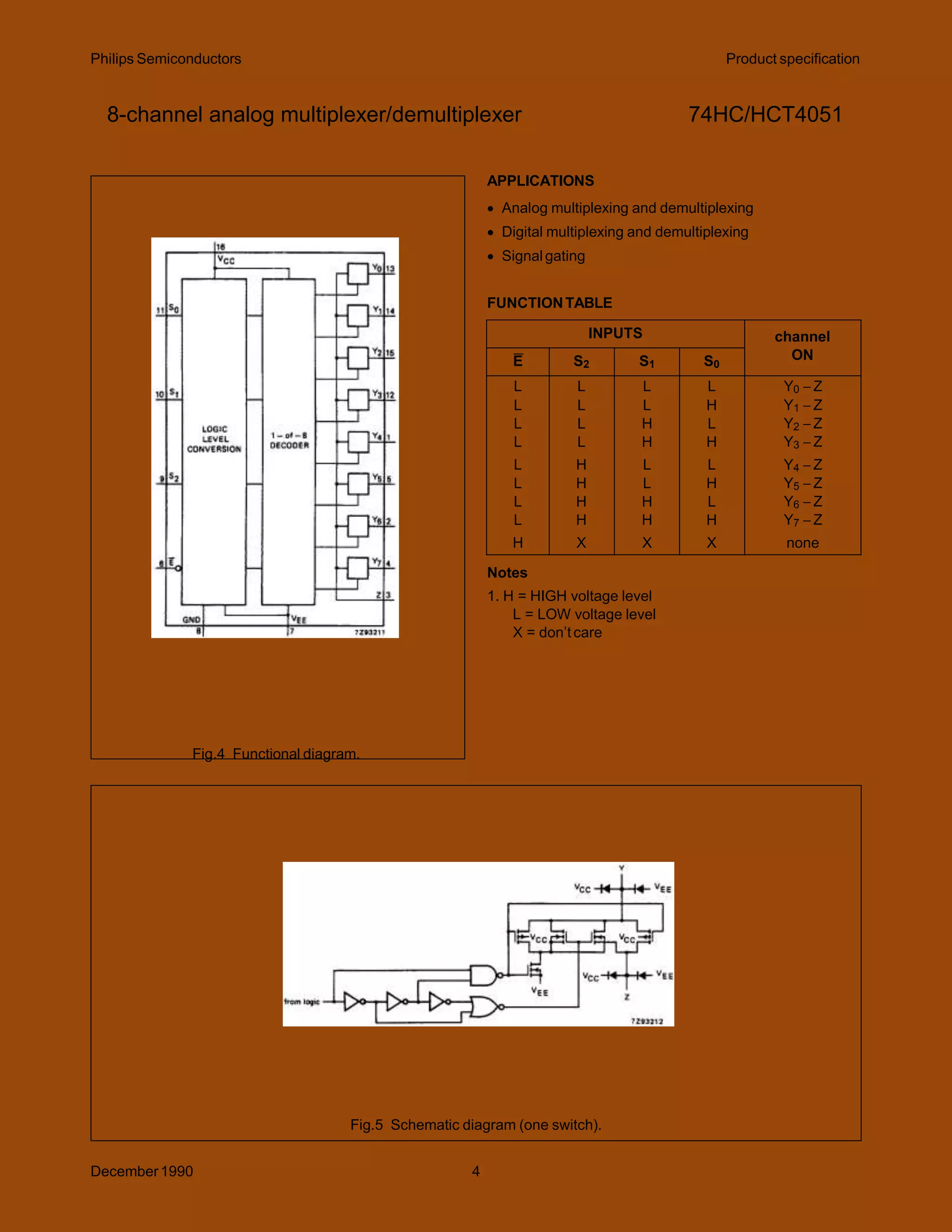
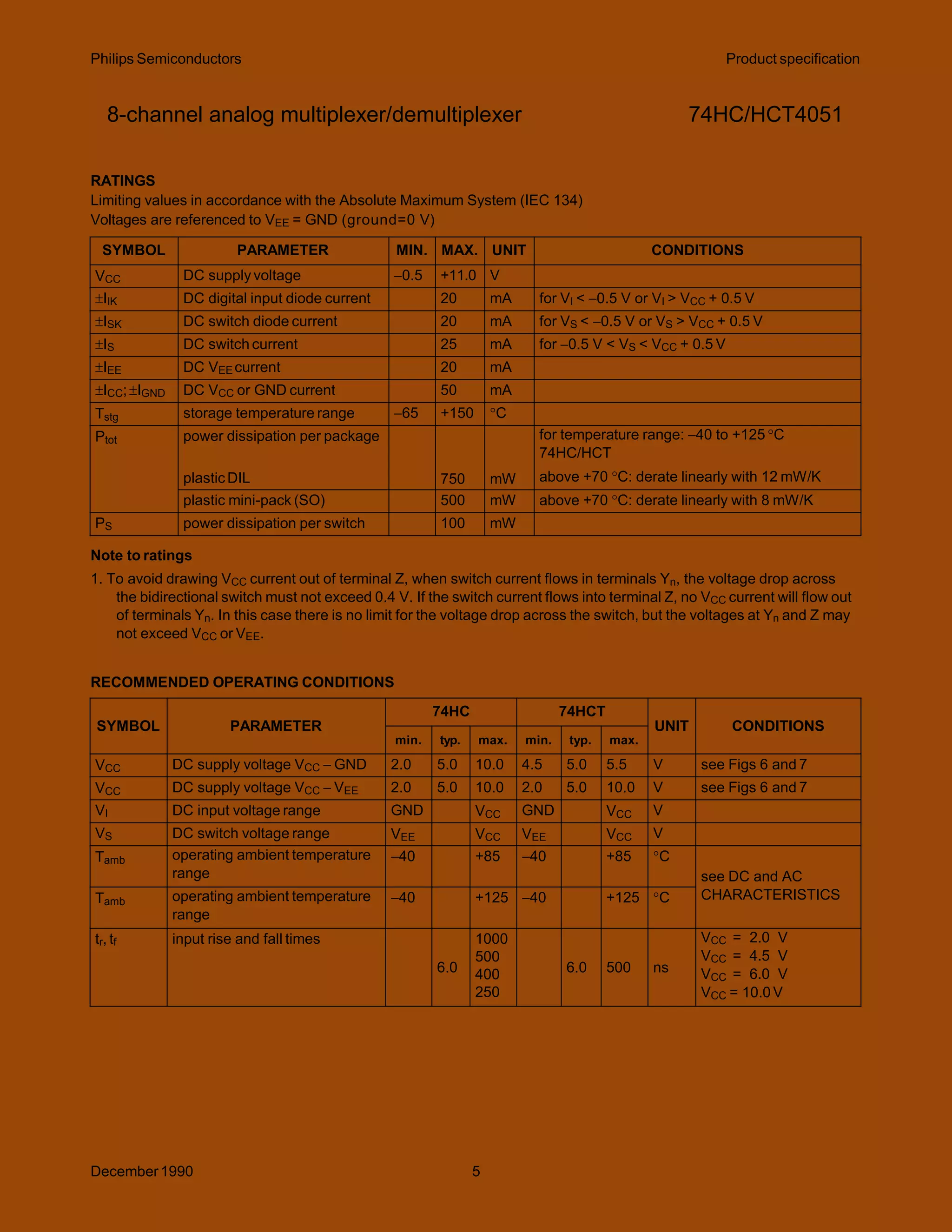
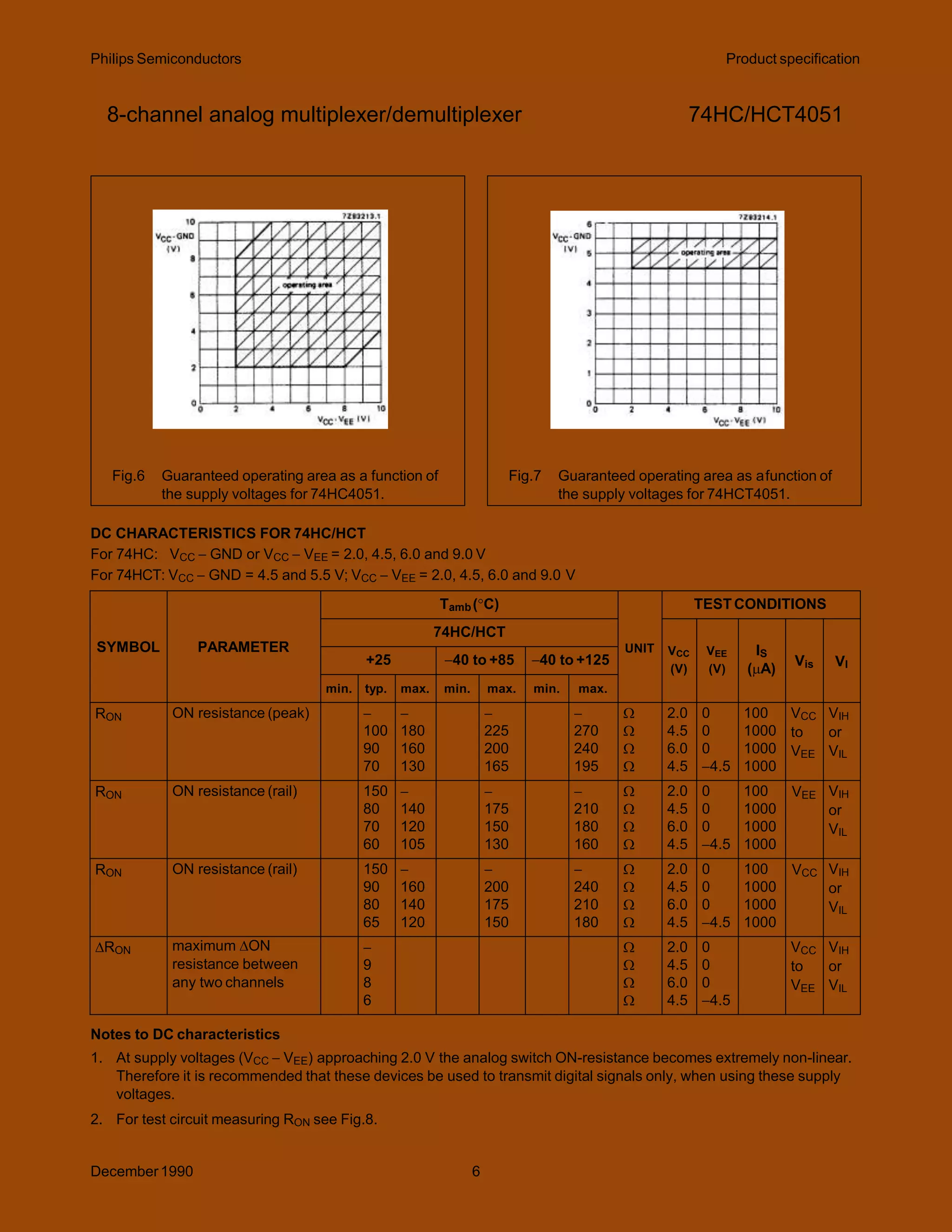
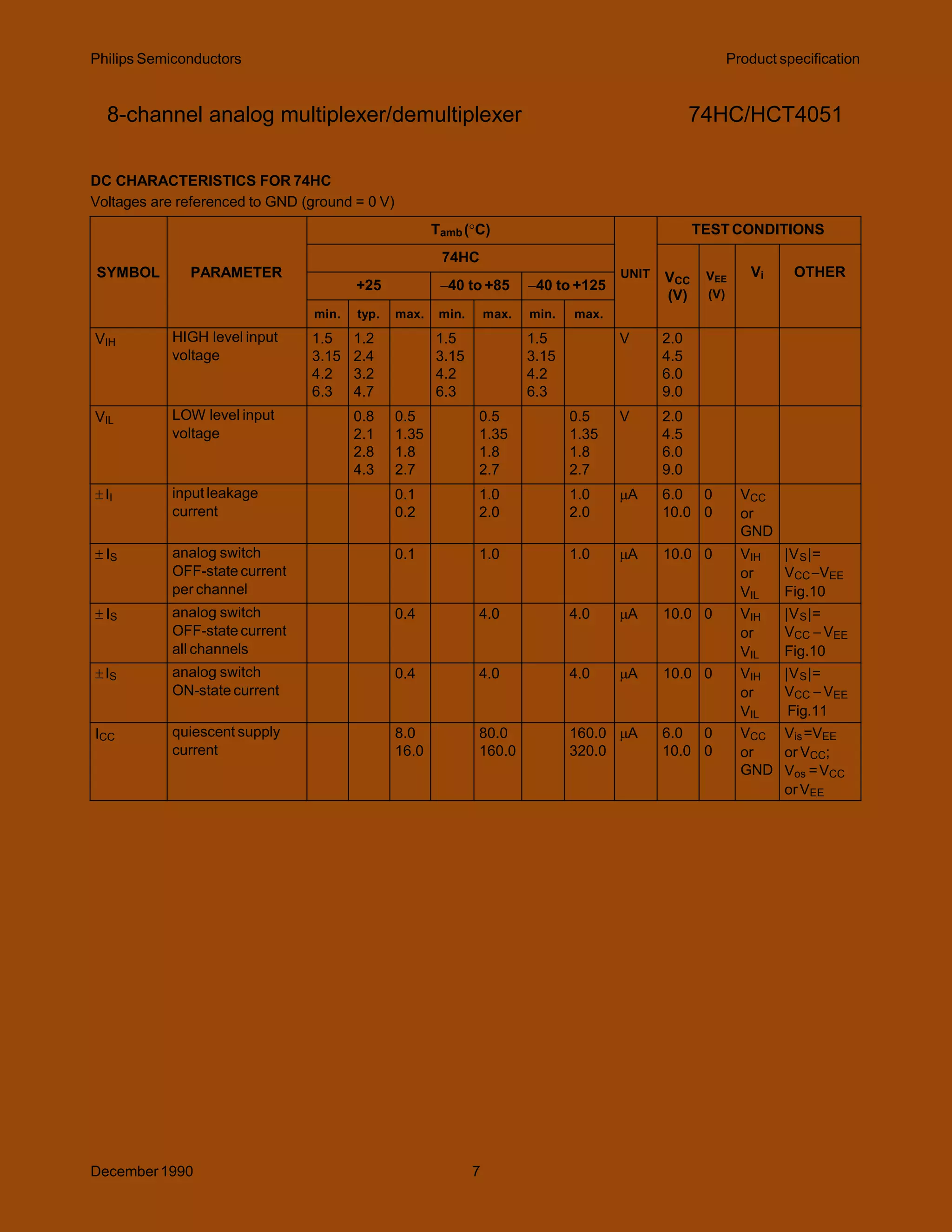
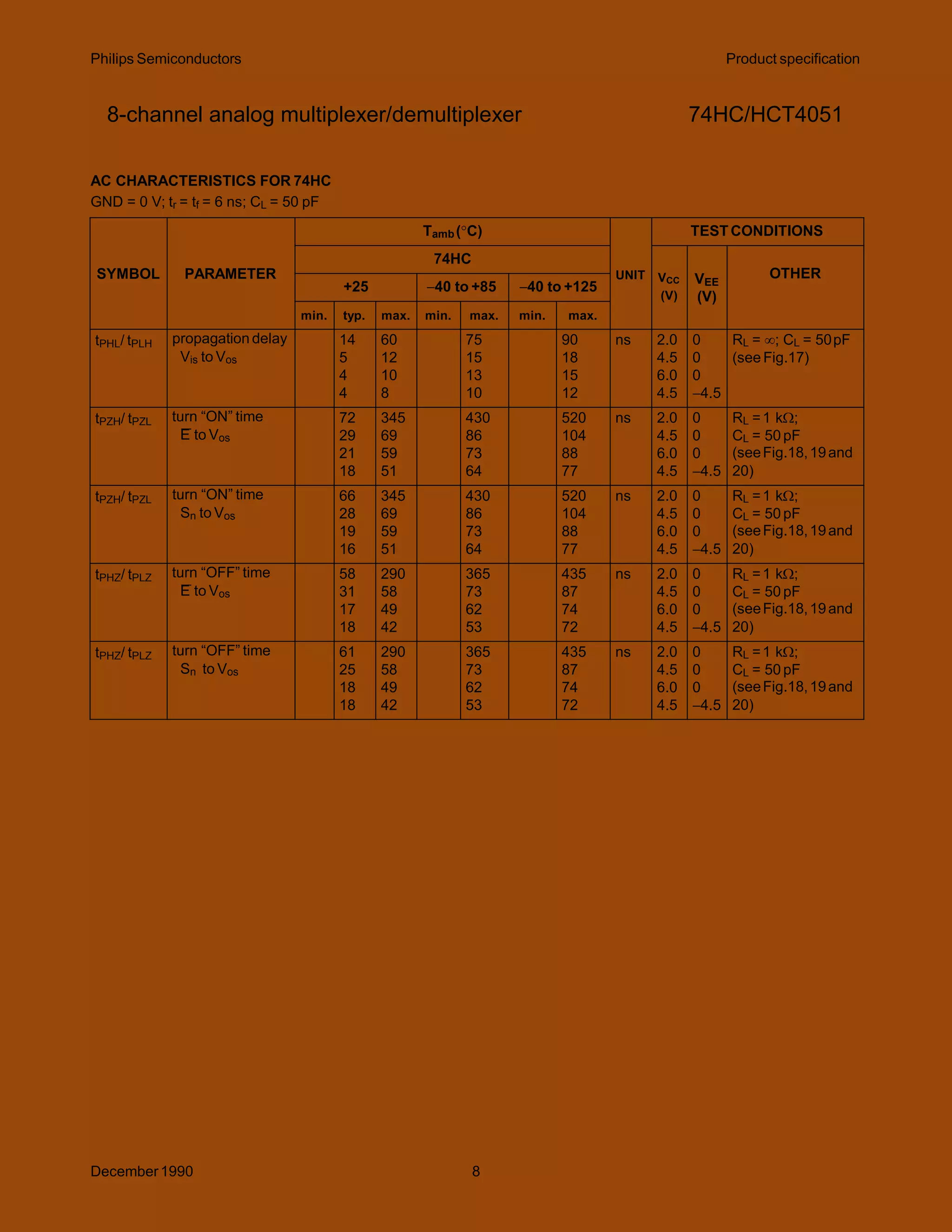
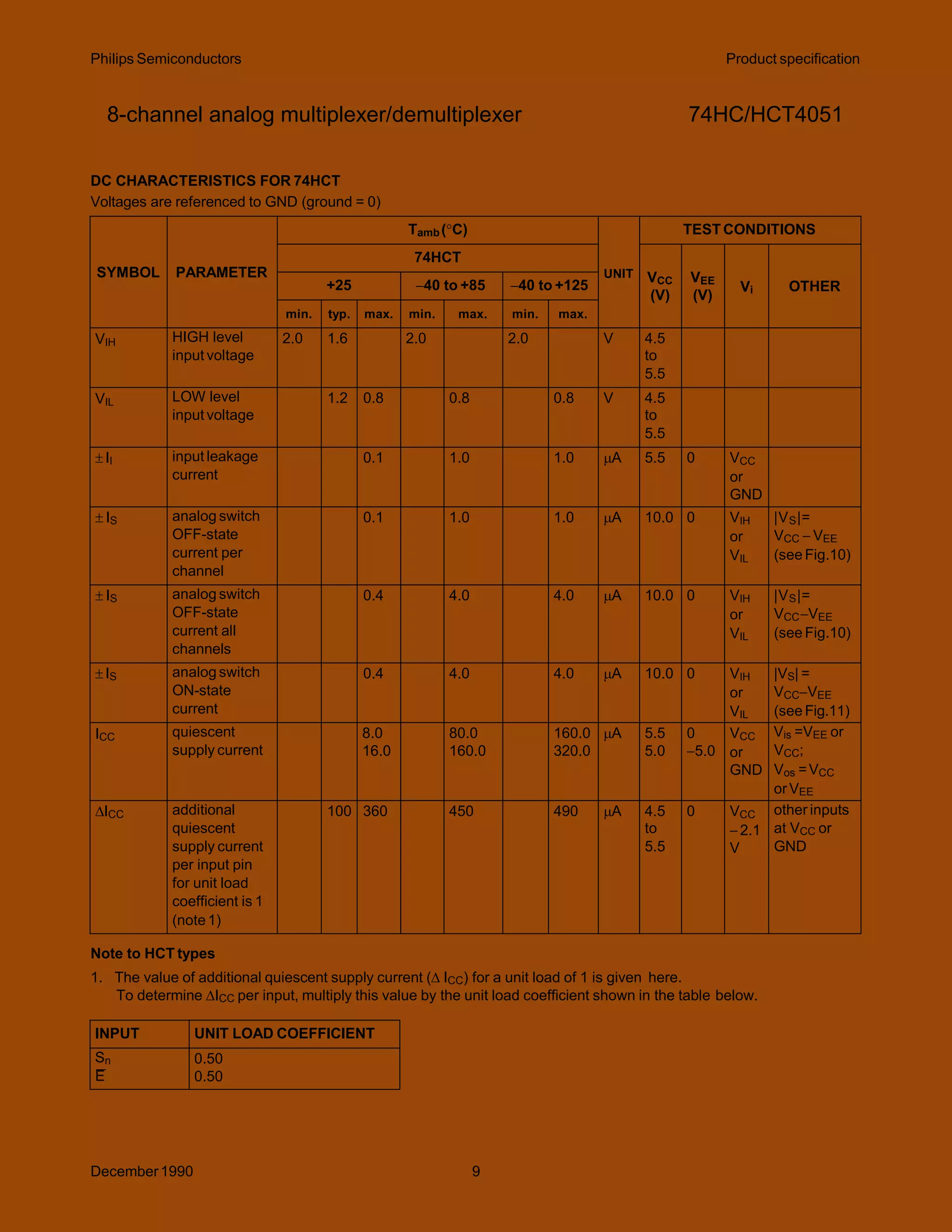


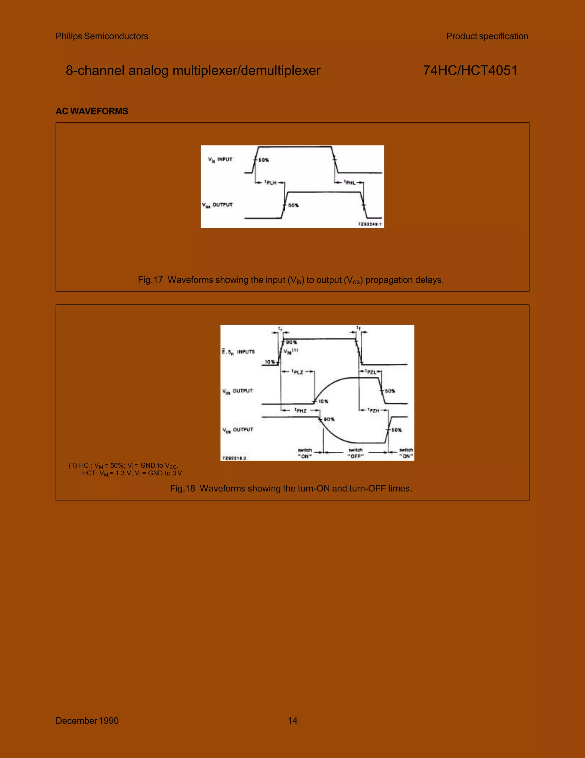


The document provides specifications for the 74HC/HCT4051 8-channel analog multiplexer/demultiplexer integrated circuit. It describes the key features and applications of the IC, which allows one of eight analog input channels to be selected via three digital select lines. Tables provide timing parameters and electrical characteristics for the analog switches and digital control inputs over operating temperature and voltage ranges. Diagrams depict the pinout, logic symbol, functional operation and truth table of the multiplexer/demultiplexer device.


