SlideShare a Scribd company logo
HCC/HCF4017B
HCC/HCF4022B
COUNTERS/DIVIDERS
.FULLY STATIC OPERATION
.MEDIUM SPEEDOPERATION-12MHz (typ.) AT
VDD = 10V
.STANDARDIZED SYMMETRICAL OUTPUT
CHARACTERISTICS
.QUIESCENT CURRENT SPECIFIED TO 20V
FOR HCC DEVICE
.INPUT CURRENT OF 100nA AT 18V AND 25°C
FOR HCC DEVICE
.100% TESTED FOR QUIESCENT CURRENT
.5V, 10V, AND 15V PARAMETRIC RATINGS
.MEETS ALLREQUIREMENTS OF JEDECTEN-
TATIVE STANDARD N° 13A, ”STANDARD
SPECIFICATIONS FOR DESCRIPTION OF ”B”
SERIES CMOS DEVICES”
June 1989
EY
(Plastic Package)
F
(Ceramic Frit Seal Package)
C1
(Plastic Chip Carrier)
ORDER CODES :
HCC40XXBF HCF40XXBM1
HCF40XXBEY HCF40XXBC1
PIN CONNECTIONS
4017B DECADE COUNTER WITH 10
DECODED OUTPUTS
4022B OCTAL COUNTER WITH 8
DECODED OUTPUTS
4017B
4022B
M1
(Micro Package)
DESCRIPTION
The HCC4017B/4022B (extended temperature
range) and HCF4017B/4022B (intermediate tem-
perature range) are monolithic integrated circuits,
available in 16-lead dual in-line plastic or ceramic
package and plastic micro package.
The HCC/HCF4017B and HCC/HCF4022B are 5-
stage and 4-stage Johnson counters having 10 and
8 decoded outputs, respectively. Inputs include a
CLOCK, a RESET, and a CLOCK INHIBIT signal.
Schmitt trigger action in the CLOCK input circuit pro-
videspulse shaping that allows unlimited clockinput
pulse rise and fall times. These counters are ad-
vanced one count at the positive clock signal tran-
sition if the CLOCK INHIBIT signal is low. Counter
advancement via the clock line is inhibited when the
CLOCKINHIBIT signalishigh. A high RESET signal
clears the counter to its zero count. Use of the
Johnson decade-counter configuration permits
high-speed operation, 2-input decimal-decode gat-
ing, and spike-free decoded outputs. Anti-lock gat-
ing is provided, thus assuring proper counting
sequence. The decoded outputs are normally low
and go high only at their respective decoded time
slot. Each decoded output remains high for one full
clock cycle. A CARRY-OUT signal completes one
1/12
FUNCTIONAL DIAGRAM
ABSOLUTE MAXIMUM RATINGS
Symbol Parameter Value Unit
VDD* Supply Voltage : HCC Types
HCF Types
– 0.5 to + 20
– 0.5 to + 18
V
V
VI Input Voltage – 0.5 to VDD + 0.5 V
II DC Input Current (any one input) ± 10 mA
Pt ot Total Power Dissipation (per package)
Dissipation per Output Transistor
for Top = Full Package-temperature Range
200
100
mW
mW
To p Operating Temperature : HCC Types
HCF Types
– 55 to + 125
– 40 to + 85
°C
°C
Tstg Storage Temperature – 65 to + 150 °C
RECOMMENDED OPERATING CONDITIONS
Symbol Parameter Value Unit
VDD Supply Voltage : HCC Types
HCF Types
3 to 18
3 to 15
V
V
VI Input Voltage 0 to VDD V
To p Operating Temperature : HCC Types
HCF Types
– 55 to + 125
– 40 to + 85
°C
°C
4022B
Stresses above those listed under ”Absolute Maximum Ratings” may cause permanent damage to the device. This is a stress
rating only and functional operation of the device at these or any other conditions above those indicated in the operational sec-
tions of this specification is not implied. Exposure to absolute maximum rating conditions for external periods may affect device
reliability.
* All voltages values are referred to VSS pin voltage.
4017B
cycle every 10 clock input cycles in the
HCC/HCF4017B or every 8 clockinput cycles in the
HCC/HCF4022B and isusedto ripple-clock the suc-
ceeding device in a multi-device counting chain.
HCC/HCF4017B/4022B
2/12
LOGIC DIAGRAMS
4017B
4022
HCC/HCF4017B/4022B
3/12
TIMING DIAGRAMS
4017B
4022B
HCC/HCF4017B/4022B
4/12
STATIC ELECTRICAL CHARACTERISTICS (over recommended operating conditions)
Test Conditions Value
VI VO | IO| VDD TLow* 25°C THigh*Symbol Parameter
(V) (V) (µA) (V) Min. Max. Min. Typ. Max. Min. Max.
Unit
IL Quiescent
Current
HCC
Types
0/ 5 5 5 0.04 5 150
µA
0/10 10 10 0.04 10 300
0/15 15 20 0.04 20 600
0/20 20 100 0.08 100 3000
HCF
Types
0/ 5 5 20 0.04 20 150
0/10 10 40 0.04 40 300
0/15 15 80 0.04 80 600
VOH Output High
Voltage
0/ 5 < 1 5 4.95 4.95 4.95
V0/10 < 1 10 9.95 9.95 9.95
0/15 < 1 15 14.95 14.95 14.95
VOL Output Low
Voltage
5/0 < 1 5 0.05 0.05 0.05
V10/0 < 1 10 0.05 0.05 0.05
15/0 < 1 15 0.05 0.05 0.05
VIH Input High
Voltage
0.5/4.5 < 1 5 3.5 3.5 3.5
V1/9 < 1 10 7 7 7
1.5/13.5 < 1 15 11 11 11
VIL Input Low
Voltage
4.5/0.5 < 1 5 1.5 1.5 1.5
V9/1 < 1 10 3 3 3
13.5/1.5 < 1 15 4 4 4
IOH Output
Drive
Current
HCC
Types
0/ 5 2.5 5 – 2 – 1.6 – 3.2 –
1.15
mA
0/ 5 4.6 5 –
0.64
–
0.51
– 1 –
0.36
0/10 9.5 10 – 1.6 – 1.3 – 2.6 – 0.9
0/15 13.5 15 – 4.2 – 3.4 – 6.8 – 2.4
HCF
Types
0/ 5 2.5 5 –
1.53
–
1.36
– 3.2 – 1.1
0/ 5 4.6 5 –
0.52
–
0.44
– 1 –
0.36
0/10 9.5 10 – 1.3 – 1.1 – 2.6 – 0.9
0/15 13.5 15 – 3.6 – 3.0 – 6.8 – 2.4
IOL Output
Sink
Current
HCC
Types
0/ 5 0.4 5 0.64 0.51 1 0.36
mA
0/10 0.5 10 1.6 1.3 2.6 0.9
0/15 1.5 15 4.2 3.4 6.8 2.4
HCF
Types
0/ 5 0.4 5 0.52 0.44 1 0.36
0/10 0.5 10 1.3 1.1 2.6 0.9
0/15 1.5 15 3.6 3.0 6.8 2.4
IIH, IIL Input
Leakage
Current
HCC
Types
0/18
Any Input
18 ± 0.1 ±10–5
± 0.1 ± 1
µA
HCF
Types
0/15 15 ± 0.3 ±10–5
± 0.3 ± 1
CI Input Capacitance Any Input 5 7.5 pF
* TLow = – 55°C for HCC device : – 40°C for HCF device.
* THigh = + 125°C for HCC device : + 85°C for HCF device.
The Noise Margin for both ”1” and ”0” level is : 1V min. width VDD = 5V, 2V min. width VDD = 10V, 2.5V min. width VDD =
15V.
HCC/HCF4017B/4022B
5/12
DYNAMIC ELECTRICAL CHARACTERISTICS (Tamb = 25°C, CL = 50pF, RL = 200kΩ,
typical temperature coefficient for all VDD = 0.3%/°C values, all input rise and fall time = 20ns)
Value
Symbol Parameter
Test Conditions
VDD (V) Min. Typ. Max.
Unit
CLOCKED OPERATION
tPLH, tPHL Propagation Delay Time
Decode Out
5 325 650
ns10 135 270
15 85 170
Carry Out 5 300 600
ns10 125 250
15 80 160
tTHL, tTLH Transition Time
Carry Out or Decoded Out Line
5 100 200
ns10 50 100
15 40 80
fCL* Maximum Clock Input Frequency 5 2.5 5 5
MHz10 5 10
15 5.5 11
tW Minimum Clock Pulse Width 5 100 200
ns10 45 90
15 30 60
tr, tf Clock Input Rise or Fall Time 5
Unlimited µs10
15
tsetup Data Setup Time
Minimum Clock Inhibit
5 115 230
ns10 50 100
15 35 7.5
RESET OPERATION
tPLH, tPHL Propagation Delay Time
Carry Out or Decode Out Lines
5 265 530
ns10 115 230
15 85 170
tW Minimum Reset Pulse Width 5 130 260
ns10 55 110
15 30 60
trem Minimum Reset Removal Time 5 200 400
ns10 140 280
15 75 150
* Measured with respect to carry output line.
HCC/HCF4017B/4022B
6/12
Typical Output Low (sink) Current Characteristics. Minimum Output Low(sink) Current Characteristics.
Typical Output High (source) Current Charac-
teristics.
Minimum Output High (source ) Current Charac-
teristics.
TYPICAL APPLICATIONS
Divide by N Counter (N ≤ 10) with N Decoded Out-
puts.
When the Nth
decoded output is reached (Nth
clock pulse) the S-R flip-flop (constructed from
two NOR gates of the HCC/HCF4001B) gener-
ates a reset pulse which clears the
HCC/HCF4017B to its zero count. At this time, if
the Nth
decoded output is greater than or equal
to 6, the COUT line goes high to clock the next
HCC/HCF4017B counter section. The ”0”
decoded output also goes high at this time. Coin-
cidence of the clock low and decoded ”0” output
high resets the S-R flip flop to enable the
HCC/HCF4017B. If the N
th
decoded output is
less than 6, the COUT line will not go high and,
therefore, cannot be used. In this case ”0”
decoded output may be used to perform the
clocking function for the next counter.
HCC/HCF4017B/4022B
7/12
Plastic DIP16 (0.25) MECHANICAL DATA
DIM.
mm inch
MIN. TYP. MAX. MIN. TYP. MAX.
a1 0.51 0.020
B 0.77 1.65 0.030 0.065
b 0.5 0.020
b1 0.25 0.010
D 20 0.787
E 8.5 0.335
e 2.54 0.100
e3 17.78 0.700
F 7.1 0.280
I 5.1 0.201
L 3.3 0.130
Z 1.27 0.050
P001C
HCC/HCF4017B/4022B
8/12
Ceramic DIP16/1 MECHANICAL DATA
DIM.
mm inch
MIN. TYP. MAX. MIN. TYP. MAX.
A 20 0.787
B 7 0.276
D 3.3 0.130
E 0.38 0.015
e3 17.78 0.700
F 2.29 2.79 0.090 0.110
G 0.4 0.55 0.016 0.022
H 1.17 1.52 0.046 0.060
L 0.22 0.31 0.009 0.012
M 0.51 1.27 0.020 0.050
N 10.3 0.406
P 7.8 8.05 0.307 0.317
Q 5.08 0.200
P053D
HCC/HCF4017B/4022B
9/12
SO16 (Narrow) MECHANICAL DATA
DIM.
mm inch
MIN. TYP. MAX. MIN. TYP. MAX.
A 1.75 0.068
a1 0.1 0.2 0.004 0.007
a2 1.65 0.064
b 0.35 0.46 0.013 0.018
b1 0.19 0.25 0.007 0.010
C 0.5 0.019
c1 45° (typ.)
D 9.8 10 0.385 0.393
E 5.8 6.2 0.228 0.244
e 1.27 0.050
e3 8.89 0.350
F 3.8 4.0 0.149 0.157
G 4.6 5.3 0.181 0.208
L 0.5 1.27 0.019 0.050
M 0.62 0.024
S 8° (max.)
P013H
HCC/HCF4017B/4022B
10/12
PLCC20 MECHANICAL DATA
DIM.
mm inch
MIN. TYP. MAX. MIN. TYP. MAX.
A 9.78 10.03 0.385 0.395
B 8.89 9.04 0.350 0.356
D 4.2 4.57 0.165 0.180
d1 2.54 0.100
d2 0.56 0.022
E 7.37 8.38 0.290 0.330
e 1.27 0.050
e3 5.08 0.200
F 0.38 0.015
G 0.101 0.004
M 1.27 0.050
M1 1.14 0.045
P027A
HCC/HCF4017B/4022B
11/12
Information furnished is believed to be accurate and reliable. However, SGS-THOMSON Microelectronics assumes no responsability for the
consequences of use of such information nor for any infringement of patents or other rights of third parties which may results from its use. No
license is granted by implication or otherwise under any patent or patent rights of SGS-THOMSON Microelectronics. Specificationsmentioned
in this publication are subject to change without notice. This publication supersedes and replaces all information previously supplied.
SGS-THOMSON Microelectronicsproductsare notauthorized foruse ascritical componentsin life support devices or systems without express
written approval of SGS-THOMSON Microelectonics.
© 1994 SGS-THOMSON Microelectronics - All Rights Reserved
SGS-THOMSON Microelectronics GROUP OF COMPANIES
Australia - Brazil - France - Germany - Hong Kong - Italy - Japan - Korea - Malaysia - Malta - Morocco - The Netherlands -
Singapore - Spain - Sweden - Switzerland - Taiwan - Thailand - United Kingdom - U.S.A
HCC/HCF4017B/4022B
12/12

More Related Content

What's hot

Puente h
Puente hPuente h
sensores y actuadores
sensores y actuadoressensores y actuadores
sensores y actuadores
FranSimp
 
Lec 03 - Combinational Logic Design
Lec 03 - Combinational Logic DesignLec 03 - Combinational Logic Design
Lec 03 - Combinational Logic Design
Vajira Thambawita
 
Manual positron1
Manual positron1Manual positron1
Manual positron1
Leandro Concatto
 
Gerbang Universal NAND dan NOR
Gerbang Universal NAND dan NORGerbang Universal NAND dan NOR
Gerbang Universal NAND dan NOR
Anarstn
 
1.3 programacion cnc.pdf
1.3 programacion cnc.pdf1.3 programacion cnc.pdf
1.3 programacion cnc.pdf
AtemexOax
 
Questões clp-automação
Questões clp-automaçãoQuestões clp-automação
Questões clp-automação
Carlos Melo
 
Linguagens De ProgramaçãO Clp
Linguagens De ProgramaçãO ClpLinguagens De ProgramaçãO Clp
Linguagens De ProgramaçãO Clp
JÚLIO PEIXOTO
 
Corrientes eléctricas estacionarias 3
Corrientes eléctricas estacionarias 3Corrientes eléctricas estacionarias 3
Corrientes eléctricas estacionarias 3
eddanohelia
 
Clp completa
Clp completaClp completa
Clp completa
panelada
 
Controlador pid para posición de un motor dc
Controlador pid para posición de un motor dcControlador pid para posición de un motor dc
Controlador pid para posición de un motor dc
Ever chipana
 
Funcionamiento de transmisor de nivel por ultrasonido
Funcionamiento de transmisor de nivel por ultrasonidoFuncionamiento de transmisor de nivel por ultrasonido
Funcionamiento de transmisor de nivel por ultrasonido
Clishman Félix Villavicencio
 
Microcontroladores: Microcontroladores PIC fundamentos y aplicaciones didácticos
Microcontroladores: Microcontroladores PIC fundamentos y aplicaciones didácticosMicrocontroladores: Microcontroladores PIC fundamentos y aplicaciones didácticos
Microcontroladores: Microcontroladores PIC fundamentos y aplicaciones didácticos
SANTIAGO PABLO ALBERTO
 
Flip Flops Parte 1
Flip Flops Parte 1Flip Flops Parte 1
Flip Flops Parte 1
Elaine Cecília Gatto
 
Laboratorio 1 Electronica de Potencia
Laboratorio 1 Electronica de PotenciaLaboratorio 1 Electronica de Potencia
Laboratorio 1 Electronica de Potencia
gino machuca
 
CLP S7 300 E S7 400
CLP S7 300 E S7 400CLP S7 300 E S7 400
CLP S7 300 E S7 400
confidencial
 
Trabajo de circuito logico restador
Trabajo de circuito logico restadorTrabajo de circuito logico restador
Trabajo de circuito logico restador
Jesus Jimenez
 
Erros e controle de malhas
Erros e controle de malhasErros e controle de malhas
Erros e controle de malhas
jomartg
 
Signal conditioning
Signal conditioningSignal conditioning
Signal conditioning
Fani Hakim
 
Eletronica digital lista i
Eletronica digital   lista iEletronica digital   lista i
Eletronica digital lista iCarlos Melo
 

What's hot (20)

Puente h
Puente hPuente h
Puente h
 
sensores y actuadores
sensores y actuadoressensores y actuadores
sensores y actuadores
 
Lec 03 - Combinational Logic Design
Lec 03 - Combinational Logic DesignLec 03 - Combinational Logic Design
Lec 03 - Combinational Logic Design
 
Manual positron1
Manual positron1Manual positron1
Manual positron1
 
Gerbang Universal NAND dan NOR
Gerbang Universal NAND dan NORGerbang Universal NAND dan NOR
Gerbang Universal NAND dan NOR
 
1.3 programacion cnc.pdf
1.3 programacion cnc.pdf1.3 programacion cnc.pdf
1.3 programacion cnc.pdf
 
Questões clp-automação
Questões clp-automaçãoQuestões clp-automação
Questões clp-automação
 
Linguagens De ProgramaçãO Clp
Linguagens De ProgramaçãO ClpLinguagens De ProgramaçãO Clp
Linguagens De ProgramaçãO Clp
 
Corrientes eléctricas estacionarias 3
Corrientes eléctricas estacionarias 3Corrientes eléctricas estacionarias 3
Corrientes eléctricas estacionarias 3
 
Clp completa
Clp completaClp completa
Clp completa
 
Controlador pid para posición de un motor dc
Controlador pid para posición de un motor dcControlador pid para posición de un motor dc
Controlador pid para posición de un motor dc
 
Funcionamiento de transmisor de nivel por ultrasonido
Funcionamiento de transmisor de nivel por ultrasonidoFuncionamiento de transmisor de nivel por ultrasonido
Funcionamiento de transmisor de nivel por ultrasonido
 
Microcontroladores: Microcontroladores PIC fundamentos y aplicaciones didácticos
Microcontroladores: Microcontroladores PIC fundamentos y aplicaciones didácticosMicrocontroladores: Microcontroladores PIC fundamentos y aplicaciones didácticos
Microcontroladores: Microcontroladores PIC fundamentos y aplicaciones didácticos
 
Flip Flops Parte 1
Flip Flops Parte 1Flip Flops Parte 1
Flip Flops Parte 1
 
Laboratorio 1 Electronica de Potencia
Laboratorio 1 Electronica de PotenciaLaboratorio 1 Electronica de Potencia
Laboratorio 1 Electronica de Potencia
 
CLP S7 300 E S7 400
CLP S7 300 E S7 400CLP S7 300 E S7 400
CLP S7 300 E S7 400
 
Trabajo de circuito logico restador
Trabajo de circuito logico restadorTrabajo de circuito logico restador
Trabajo de circuito logico restador
 
Erros e controle de malhas
Erros e controle de malhasErros e controle de malhas
Erros e controle de malhas
 
Signal conditioning
Signal conditioningSignal conditioning
Signal conditioning
 
Eletronica digital lista i
Eletronica digital   lista iEletronica digital   lista i
Eletronica digital lista i
 

Similar to Hcf4017 be

Original Analog Switch IC CD74HC4066PWR SN74HC4066DR 4066DR 4066PWR 4066 SOP...
Original Analog Switch IC CD74HC4066PWR  SN74HC4066DR 4066DR 4066PWR 4066 SOP...Original Analog Switch IC CD74HC4066PWR  SN74HC4066DR 4066DR 4066PWR 4066 SOP...
Original Analog Switch IC CD74HC4066PWR SN74HC4066DR 4066DR 4066PWR 4066 SOP...
AUTHELECTRONIC
 
Cd4051 ti
Cd4051 tiCd4051 ti
Cd4051 ti
Hugo Alaniz
 
Voltage to-frequency and frequency-to-voltage converter
Voltage to-frequency and frequency-to-voltage converterVoltage to-frequency and frequency-to-voltage converter
Voltage to-frequency and frequency-to-voltage converter
The Hoa Nguyen
 
ACPL-K49T - Datasheet - Broadcom Corporation
ACPL-K49T - Datasheet - Broadcom CorporationACPL-K49T - Datasheet - Broadcom Corporation
ACPL-K49T - Datasheet - Broadcom Corporation
MarioFarias18
 
Hdd15 5-ag-power-one
Hdd15 5-ag-power-oneHdd15 5-ag-power-one
Hdd15 5-ag-power-onePawar Chander
 
2600T Series Pressure Transmitter Model 261GS Gauge Model 261AS Absolute stan...
2600T Series Pressure Transmitter Model 261GS Gauge Model 261AS Absolute stan...2600T Series Pressure Transmitter Model 261GS Gauge Model 261AS Absolute stan...
2600T Series Pressure Transmitter Model 261GS Gauge Model 261AS Absolute stan...
Michael Sun
 
2600T Series Pressure Transmitter Model 261GS Gauge Model 261AS Absolute stan...
2600T Series Pressure Transmitter Model 261GS Gauge Model 261AS Absolute stan...2600T Series Pressure Transmitter Model 261GS Gauge Model 261AS Absolute stan...
2600T Series Pressure Transmitter Model 261GS Gauge Model 261AS Absolute stan...
Michael Sun
 
110 MSPS/140 MSPS Analog Interface
110 MSPS/140 MSPS Analog Interface110 MSPS/140 MSPS Analog Interface
110 MSPS/140 MSPS Analog Interface
Hua Duy Tien
 
Datasheet H164
Datasheet  H164Datasheet  H164
Datasheet H164
Emanuel Manuel
 
RT7257E Datasheet PDF
RT7257E Datasheet PDFRT7257E Datasheet PDF
RT7257E Datasheet PDF
Datasheet Bank
 
Integrated circuit (data sheet)
Integrated circuit (data sheet)Integrated circuit (data sheet)
Integrated circuit (data sheet)
St. Xavier's college, maitighar,Kathmandu
 
SFH6916_08 - Datasheet - VISHAY
SFH6916_08 - Datasheet - VISHAYSFH6916_08 - Datasheet - VISHAY
SFH6916_08 - Datasheet - VISHAY
MarioFarias18
 
Advanced motion controls b100a400ac
Advanced motion controls b100a400acAdvanced motion controls b100a400ac
Advanced motion controls b100a400ac
Electromate
 
Original Opto PC957L PC957 P957 957 DIP-8 New Sharp
Original Opto PC957L PC957 P957 957 DIP-8 New SharpOriginal Opto PC957L PC957 P957 957 DIP-8 New Sharp
Original Opto PC957L PC957 P957 957 DIP-8 New Sharp
authelectroniccom
 
Advanced motion controls azbh60a8
Advanced motion controls azbh60a8Advanced motion controls azbh60a8
Advanced motion controls azbh60a8
Electromate
 
Advanced motion controls azxbe15a8
Advanced motion controls azxbe15a8Advanced motion controls azxbe15a8
Advanced motion controls azxbe15a8
Electromate
 

Similar to Hcf4017 be (20)

Original Analog Switch IC CD74HC4066PWR SN74HC4066DR 4066DR 4066PWR 4066 SOP...
Original Analog Switch IC CD74HC4066PWR  SN74HC4066DR 4066DR 4066PWR 4066 SOP...Original Analog Switch IC CD74HC4066PWR  SN74HC4066DR 4066DR 4066PWR 4066 SOP...
Original Analog Switch IC CD74HC4066PWR SN74HC4066DR 4066DR 4066PWR 4066 SOP...
 
Cd4051 ti
Cd4051 tiCd4051 ti
Cd4051 ti
 
74164
7416474164
74164
 
Voltage to-frequency and frequency-to-voltage converter
Voltage to-frequency and frequency-to-voltage converterVoltage to-frequency and frequency-to-voltage converter
Voltage to-frequency and frequency-to-voltage converter
 
Ucc 3895 dw
Ucc 3895 dwUcc 3895 dw
Ucc 3895 dw
 
ACPL-K49T - Datasheet - Broadcom Corporation
ACPL-K49T - Datasheet - Broadcom CorporationACPL-K49T - Datasheet - Broadcom Corporation
ACPL-K49T - Datasheet - Broadcom Corporation
 
Hdd15 5-ag-power-one
Hdd15 5-ag-power-oneHdd15 5-ag-power-one
Hdd15 5-ag-power-one
 
2600T Series Pressure Transmitter Model 261GS Gauge Model 261AS Absolute stan...
2600T Series Pressure Transmitter Model 261GS Gauge Model 261AS Absolute stan...2600T Series Pressure Transmitter Model 261GS Gauge Model 261AS Absolute stan...
2600T Series Pressure Transmitter Model 261GS Gauge Model 261AS Absolute stan...
 
2600T Series Pressure Transmitter Model 261GS Gauge Model 261AS Absolute stan...
2600T Series Pressure Transmitter Model 261GS Gauge Model 261AS Absolute stan...2600T Series Pressure Transmitter Model 261GS Gauge Model 261AS Absolute stan...
2600T Series Pressure Transmitter Model 261GS Gauge Model 261AS Absolute stan...
 
110 MSPS/140 MSPS Analog Interface
110 MSPS/140 MSPS Analog Interface110 MSPS/140 MSPS Analog Interface
110 MSPS/140 MSPS Analog Interface
 
38 hc43ym
38 hc43ym38 hc43ym
38 hc43ym
 
Datasheet H164
Datasheet  H164Datasheet  H164
Datasheet H164
 
RT7257E Datasheet PDF
RT7257E Datasheet PDFRT7257E Datasheet PDF
RT7257E Datasheet PDF
 
Tl 2844 b
Tl 2844 bTl 2844 b
Tl 2844 b
 
Integrated circuit (data sheet)
Integrated circuit (data sheet)Integrated circuit (data sheet)
Integrated circuit (data sheet)
 
SFH6916_08 - Datasheet - VISHAY
SFH6916_08 - Datasheet - VISHAYSFH6916_08 - Datasheet - VISHAY
SFH6916_08 - Datasheet - VISHAY
 
Advanced motion controls b100a400ac
Advanced motion controls b100a400acAdvanced motion controls b100a400ac
Advanced motion controls b100a400ac
 
Original Opto PC957L PC957 P957 957 DIP-8 New Sharp
Original Opto PC957L PC957 P957 957 DIP-8 New SharpOriginal Opto PC957L PC957 P957 957 DIP-8 New Sharp
Original Opto PC957L PC957 P957 957 DIP-8 New Sharp
 
Advanced motion controls azbh60a8
Advanced motion controls azbh60a8Advanced motion controls azbh60a8
Advanced motion controls azbh60a8
 
Advanced motion controls azxbe15a8
Advanced motion controls azxbe15a8Advanced motion controls azxbe15a8
Advanced motion controls azxbe15a8
 

Recently uploaded

一比一原版SDSU毕业证圣地亚哥州立大学毕业证成绩单如何办理
一比一原版SDSU毕业证圣地亚哥州立大学毕业证成绩单如何办理一比一原版SDSU毕业证圣地亚哥州立大学毕业证成绩单如何办理
一比一原版SDSU毕业证圣地亚哥州立大学毕业证成绩单如何办理
kywwoyk
 
web-tech-lab-manual-final-abhas.pdf. Jer
web-tech-lab-manual-final-abhas.pdf. Jerweb-tech-lab-manual-final-abhas.pdf. Jer
web-tech-lab-manual-final-abhas.pdf. Jer
freshgammer09
 
NO1 Uk Amil Baba In Lahore Kala Jadu In Lahore Best Amil In Lahore Amil In La...
NO1 Uk Amil Baba In Lahore Kala Jadu In Lahore Best Amil In Lahore Amil In La...NO1 Uk Amil Baba In Lahore Kala Jadu In Lahore Best Amil In Lahore Amil In La...
NO1 Uk Amil Baba In Lahore Kala Jadu In Lahore Best Amil In Lahore Amil In La...
Amil baba
 
Drugs used in parkinsonism and other movement disorders.pptx
Drugs used in parkinsonism and other movement disorders.pptxDrugs used in parkinsonism and other movement disorders.pptx
Drugs used in parkinsonism and other movement disorders.pptx
ThalapathyVijay15
 
MATHEMATICS BRIDGE COURSE (TEN DAYS PLANNER) (FOR CLASS XI STUDENTS GOING TO ...
MATHEMATICS BRIDGE COURSE (TEN DAYS PLANNER) (FOR CLASS XI STUDENTS GOING TO ...MATHEMATICS BRIDGE COURSE (TEN DAYS PLANNER) (FOR CLASS XI STUDENTS GOING TO ...
MATHEMATICS BRIDGE COURSE (TEN DAYS PLANNER) (FOR CLASS XI STUDENTS GOING TO ...
PinkySharma900491
 
一比一原版UVM毕业证佛蒙特大学毕业证成绩单如何办理
一比一原版UVM毕业证佛蒙特大学毕业证成绩单如何办理一比一原版UVM毕业证佛蒙特大学毕业证成绩单如何办理
一比一原版UVM毕业证佛蒙特大学毕业证成绩单如何办理
kywwoyk
 
一比一原版SDSU毕业证圣地亚哥州立大学毕业证成绩单如何办理
一比一原版SDSU毕业证圣地亚哥州立大学毕业证成绩单如何办理一比一原版SDSU毕业证圣地亚哥州立大学毕业证成绩单如何办理
一比一原版SDSU毕业证圣地亚哥州立大学毕业证成绩单如何办理
eemet
 
Cyber Sequrity.pptx is life of cyber security
Cyber Sequrity.pptx is life of cyber securityCyber Sequrity.pptx is life of cyber security
Cyber Sequrity.pptx is life of cyber security
perweeng31
 
F5 LTM TROUBLESHOOTING Guide latest.pptx
F5 LTM TROUBLESHOOTING Guide latest.pptxF5 LTM TROUBLESHOOTING Guide latest.pptx
F5 LTM TROUBLESHOOTING Guide latest.pptx
ArjunJain44
 

Recently uploaded (9)

一比一原版SDSU毕业证圣地亚哥州立大学毕业证成绩单如何办理
一比一原版SDSU毕业证圣地亚哥州立大学毕业证成绩单如何办理一比一原版SDSU毕业证圣地亚哥州立大学毕业证成绩单如何办理
一比一原版SDSU毕业证圣地亚哥州立大学毕业证成绩单如何办理
 
web-tech-lab-manual-final-abhas.pdf. Jer
web-tech-lab-manual-final-abhas.pdf. Jerweb-tech-lab-manual-final-abhas.pdf. Jer
web-tech-lab-manual-final-abhas.pdf. Jer
 
NO1 Uk Amil Baba In Lahore Kala Jadu In Lahore Best Amil In Lahore Amil In La...
NO1 Uk Amil Baba In Lahore Kala Jadu In Lahore Best Amil In Lahore Amil In La...NO1 Uk Amil Baba In Lahore Kala Jadu In Lahore Best Amil In Lahore Amil In La...
NO1 Uk Amil Baba In Lahore Kala Jadu In Lahore Best Amil In Lahore Amil In La...
 
Drugs used in parkinsonism and other movement disorders.pptx
Drugs used in parkinsonism and other movement disorders.pptxDrugs used in parkinsonism and other movement disorders.pptx
Drugs used in parkinsonism and other movement disorders.pptx
 
MATHEMATICS BRIDGE COURSE (TEN DAYS PLANNER) (FOR CLASS XI STUDENTS GOING TO ...
MATHEMATICS BRIDGE COURSE (TEN DAYS PLANNER) (FOR CLASS XI STUDENTS GOING TO ...MATHEMATICS BRIDGE COURSE (TEN DAYS PLANNER) (FOR CLASS XI STUDENTS GOING TO ...
MATHEMATICS BRIDGE COURSE (TEN DAYS PLANNER) (FOR CLASS XI STUDENTS GOING TO ...
 
一比一原版UVM毕业证佛蒙特大学毕业证成绩单如何办理
一比一原版UVM毕业证佛蒙特大学毕业证成绩单如何办理一比一原版UVM毕业证佛蒙特大学毕业证成绩单如何办理
一比一原版UVM毕业证佛蒙特大学毕业证成绩单如何办理
 
一比一原版SDSU毕业证圣地亚哥州立大学毕业证成绩单如何办理
一比一原版SDSU毕业证圣地亚哥州立大学毕业证成绩单如何办理一比一原版SDSU毕业证圣地亚哥州立大学毕业证成绩单如何办理
一比一原版SDSU毕业证圣地亚哥州立大学毕业证成绩单如何办理
 
Cyber Sequrity.pptx is life of cyber security
Cyber Sequrity.pptx is life of cyber securityCyber Sequrity.pptx is life of cyber security
Cyber Sequrity.pptx is life of cyber security
 
F5 LTM TROUBLESHOOTING Guide latest.pptx
F5 LTM TROUBLESHOOTING Guide latest.pptxF5 LTM TROUBLESHOOTING Guide latest.pptx
F5 LTM TROUBLESHOOTING Guide latest.pptx
 

Hcf4017 be

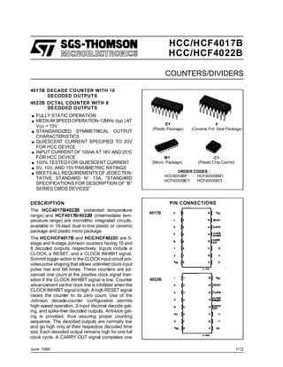
  • 1. HCC/HCF4017B HCC/HCF4022B COUNTERS/DIVIDERS .FULLY STATIC OPERATION .MEDIUM SPEEDOPERATION-12MHz (typ.) AT VDD = 10V .STANDARDIZED SYMMETRICAL OUTPUT CHARACTERISTICS .QUIESCENT CURRENT SPECIFIED TO 20V FOR HCC DEVICE .INPUT CURRENT OF 100nA AT 18V AND 25°C FOR HCC DEVICE .100% TESTED FOR QUIESCENT CURRENT .5V, 10V, AND 15V PARAMETRIC RATINGS .MEETS ALLREQUIREMENTS OF JEDECTEN- TATIVE STANDARD N° 13A, ”STANDARD SPECIFICATIONS FOR DESCRIPTION OF ”B” SERIES CMOS DEVICES” June 1989 EY (Plastic Package) F (Ceramic Frit Seal Package) C1 (Plastic Chip Carrier) ORDER CODES : HCC40XXBF HCF40XXBM1 HCF40XXBEY HCF40XXBC1 PIN CONNECTIONS 4017B DECADE COUNTER WITH 10 DECODED OUTPUTS 4022B OCTAL COUNTER WITH 8 DECODED OUTPUTS 4017B 4022B M1 (Micro Package) DESCRIPTION The HCC4017B/4022B (extended temperature range) and HCF4017B/4022B (intermediate tem- perature range) are monolithic integrated circuits, available in 16-lead dual in-line plastic or ceramic package and plastic micro package. The HCC/HCF4017B and HCC/HCF4022B are 5- stage and 4-stage Johnson counters having 10 and 8 decoded outputs, respectively. Inputs include a CLOCK, a RESET, and a CLOCK INHIBIT signal. Schmitt trigger action in the CLOCK input circuit pro- videspulse shaping that allows unlimited clockinput pulse rise and fall times. These counters are ad- vanced one count at the positive clock signal tran- sition if the CLOCK INHIBIT signal is low. Counter advancement via the clock line is inhibited when the CLOCKINHIBIT signalishigh. A high RESET signal clears the counter to its zero count. Use of the Johnson decade-counter configuration permits high-speed operation, 2-input decimal-decode gat- ing, and spike-free decoded outputs. Anti-lock gat- ing is provided, thus assuring proper counting sequence. The decoded outputs are normally low and go high only at their respective decoded time slot. Each decoded output remains high for one full clock cycle. A CARRY-OUT signal completes one 1/12
  • 2. FUNCTIONAL DIAGRAM ABSOLUTE MAXIMUM RATINGS Symbol Parameter Value Unit VDD* Supply Voltage : HCC Types HCF Types – 0.5 to + 20 – 0.5 to + 18 V V VI Input Voltage – 0.5 to VDD + 0.5 V II DC Input Current (any one input) ± 10 mA Pt ot Total Power Dissipation (per package) Dissipation per Output Transistor for Top = Full Package-temperature Range 200 100 mW mW To p Operating Temperature : HCC Types HCF Types – 55 to + 125 – 40 to + 85 °C °C Tstg Storage Temperature – 65 to + 150 °C RECOMMENDED OPERATING CONDITIONS Symbol Parameter Value Unit VDD Supply Voltage : HCC Types HCF Types 3 to 18 3 to 15 V V VI Input Voltage 0 to VDD V To p Operating Temperature : HCC Types HCF Types – 55 to + 125 – 40 to + 85 °C °C 4022B Stresses above those listed under ”Absolute Maximum Ratings” may cause permanent damage to the device. This is a stress rating only and functional operation of the device at these or any other conditions above those indicated in the operational sec- tions of this specification is not implied. Exposure to absolute maximum rating conditions for external periods may affect device reliability. * All voltages values are referred to VSS pin voltage. 4017B cycle every 10 clock input cycles in the HCC/HCF4017B or every 8 clockinput cycles in the HCC/HCF4022B and isusedto ripple-clock the suc- ceeding device in a multi-device counting chain. HCC/HCF4017B/4022B 2/12
  • 5. STATIC ELECTRICAL CHARACTERISTICS (over recommended operating conditions) Test Conditions Value VI VO | IO| VDD TLow* 25°C THigh*Symbol Parameter (V) (V) (µA) (V) Min. Max. Min. Typ. Max. Min. Max. Unit IL Quiescent Current HCC Types 0/ 5 5 5 0.04 5 150 µA 0/10 10 10 0.04 10 300 0/15 15 20 0.04 20 600 0/20 20 100 0.08 100 3000 HCF Types 0/ 5 5 20 0.04 20 150 0/10 10 40 0.04 40 300 0/15 15 80 0.04 80 600 VOH Output High Voltage 0/ 5 < 1 5 4.95 4.95 4.95 V0/10 < 1 10 9.95 9.95 9.95 0/15 < 1 15 14.95 14.95 14.95 VOL Output Low Voltage 5/0 < 1 5 0.05 0.05 0.05 V10/0 < 1 10 0.05 0.05 0.05 15/0 < 1 15 0.05 0.05 0.05 VIH Input High Voltage 0.5/4.5 < 1 5 3.5 3.5 3.5 V1/9 < 1 10 7 7 7 1.5/13.5 < 1 15 11 11 11 VIL Input Low Voltage 4.5/0.5 < 1 5 1.5 1.5 1.5 V9/1 < 1 10 3 3 3 13.5/1.5 < 1 15 4 4 4 IOH Output Drive Current HCC Types 0/ 5 2.5 5 – 2 – 1.6 – 3.2 – 1.15 mA 0/ 5 4.6 5 – 0.64 – 0.51 – 1 – 0.36 0/10 9.5 10 – 1.6 – 1.3 – 2.6 – 0.9 0/15 13.5 15 – 4.2 – 3.4 – 6.8 – 2.4 HCF Types 0/ 5 2.5 5 – 1.53 – 1.36 – 3.2 – 1.1 0/ 5 4.6 5 – 0.52 – 0.44 – 1 – 0.36 0/10 9.5 10 – 1.3 – 1.1 – 2.6 – 0.9 0/15 13.5 15 – 3.6 – 3.0 – 6.8 – 2.4 IOL Output Sink Current HCC Types 0/ 5 0.4 5 0.64 0.51 1 0.36 mA 0/10 0.5 10 1.6 1.3 2.6 0.9 0/15 1.5 15 4.2 3.4 6.8 2.4 HCF Types 0/ 5 0.4 5 0.52 0.44 1 0.36 0/10 0.5 10 1.3 1.1 2.6 0.9 0/15 1.5 15 3.6 3.0 6.8 2.4 IIH, IIL Input Leakage Current HCC Types 0/18 Any Input 18 ± 0.1 ±10–5 ± 0.1 ± 1 µA HCF Types 0/15 15 ± 0.3 ±10–5 ± 0.3 ± 1 CI Input Capacitance Any Input 5 7.5 pF * TLow = – 55°C for HCC device : – 40°C for HCF device. * THigh = + 125°C for HCC device : + 85°C for HCF device. The Noise Margin for both ”1” and ”0” level is : 1V min. width VDD = 5V, 2V min. width VDD = 10V, 2.5V min. width VDD = 15V. HCC/HCF4017B/4022B 5/12
  • 6. DYNAMIC ELECTRICAL CHARACTERISTICS (Tamb = 25°C, CL = 50pF, RL = 200kΩ, typical temperature coefficient for all VDD = 0.3%/°C values, all input rise and fall time = 20ns) Value Symbol Parameter Test Conditions VDD (V) Min. Typ. Max. Unit CLOCKED OPERATION tPLH, tPHL Propagation Delay Time Decode Out 5 325 650 ns10 135 270 15 85 170 Carry Out 5 300 600 ns10 125 250 15 80 160 tTHL, tTLH Transition Time Carry Out or Decoded Out Line 5 100 200 ns10 50 100 15 40 80 fCL* Maximum Clock Input Frequency 5 2.5 5 5 MHz10 5 10 15 5.5 11 tW Minimum Clock Pulse Width 5 100 200 ns10 45 90 15 30 60 tr, tf Clock Input Rise or Fall Time 5 Unlimited µs10 15 tsetup Data Setup Time Minimum Clock Inhibit 5 115 230 ns10 50 100 15 35 7.5 RESET OPERATION tPLH, tPHL Propagation Delay Time Carry Out or Decode Out Lines 5 265 530 ns10 115 230 15 85 170 tW Minimum Reset Pulse Width 5 130 260 ns10 55 110 15 30 60 trem Minimum Reset Removal Time 5 200 400 ns10 140 280 15 75 150 * Measured with respect to carry output line. HCC/HCF4017B/4022B 6/12
  • 7. Typical Output Low (sink) Current Characteristics. Minimum Output Low(sink) Current Characteristics. Typical Output High (source) Current Charac- teristics. Minimum Output High (source ) Current Charac- teristics. TYPICAL APPLICATIONS Divide by N Counter (N ≤ 10) with N Decoded Out- puts. When the Nth decoded output is reached (Nth clock pulse) the S-R flip-flop (constructed from two NOR gates of the HCC/HCF4001B) gener- ates a reset pulse which clears the HCC/HCF4017B to its zero count. At this time, if the Nth decoded output is greater than or equal to 6, the COUT line goes high to clock the next HCC/HCF4017B counter section. The ”0” decoded output also goes high at this time. Coin- cidence of the clock low and decoded ”0” output high resets the S-R flip flop to enable the HCC/HCF4017B. If the N th decoded output is less than 6, the COUT line will not go high and, therefore, cannot be used. In this case ”0” decoded output may be used to perform the clocking function for the next counter. HCC/HCF4017B/4022B 7/12
  • 8. Plastic DIP16 (0.25) MECHANICAL DATA DIM. mm inch MIN. TYP. MAX. MIN. TYP. MAX. a1 0.51 0.020 B 0.77 1.65 0.030 0.065 b 0.5 0.020 b1 0.25 0.010 D 20 0.787 E 8.5 0.335 e 2.54 0.100 e3 17.78 0.700 F 7.1 0.280 I 5.1 0.201 L 3.3 0.130 Z 1.27 0.050 P001C HCC/HCF4017B/4022B 8/12
  • 9. Ceramic DIP16/1 MECHANICAL DATA DIM. mm inch MIN. TYP. MAX. MIN. TYP. MAX. A 20 0.787 B 7 0.276 D 3.3 0.130 E 0.38 0.015 e3 17.78 0.700 F 2.29 2.79 0.090 0.110 G 0.4 0.55 0.016 0.022 H 1.17 1.52 0.046 0.060 L 0.22 0.31 0.009 0.012 M 0.51 1.27 0.020 0.050 N 10.3 0.406 P 7.8 8.05 0.307 0.317 Q 5.08 0.200 P053D HCC/HCF4017B/4022B 9/12
  • 10. SO16 (Narrow) MECHANICAL DATA DIM. mm inch MIN. TYP. MAX. MIN. TYP. MAX. A 1.75 0.068 a1 0.1 0.2 0.004 0.007 a2 1.65 0.064 b 0.35 0.46 0.013 0.018 b1 0.19 0.25 0.007 0.010 C 0.5 0.019 c1 45° (typ.) D 9.8 10 0.385 0.393 E 5.8 6.2 0.228 0.244 e 1.27 0.050 e3 8.89 0.350 F 3.8 4.0 0.149 0.157 G 4.6 5.3 0.181 0.208 L 0.5 1.27 0.019 0.050 M 0.62 0.024 S 8° (max.) P013H HCC/HCF4017B/4022B 10/12
  • 11. PLCC20 MECHANICAL DATA DIM. mm inch MIN. TYP. MAX. MIN. TYP. MAX. A 9.78 10.03 0.385 0.395 B 8.89 9.04 0.350 0.356 D 4.2 4.57 0.165 0.180 d1 2.54 0.100 d2 0.56 0.022 E 7.37 8.38 0.290 0.330 e 1.27 0.050 e3 5.08 0.200 F 0.38 0.015 G 0.101 0.004 M 1.27 0.050 M1 1.14 0.045 P027A HCC/HCF4017B/4022B 11/12
  • 12. Information furnished is believed to be accurate and reliable. However, SGS-THOMSON Microelectronics assumes no responsability for the consequences of use of such information nor for any infringement of patents or other rights of third parties which may results from its use. No license is granted by implication or otherwise under any patent or patent rights of SGS-THOMSON Microelectronics. Specificationsmentioned in this publication are subject to change without notice. This publication supersedes and replaces all information previously supplied. SGS-THOMSON Microelectronicsproductsare notauthorized foruse ascritical componentsin life support devices or systems without express written approval of SGS-THOMSON Microelectonics. © 1994 SGS-THOMSON Microelectronics - All Rights Reserved SGS-THOMSON Microelectronics GROUP OF COMPANIES Australia - Brazil - France - Germany - Hong Kong - Italy - Japan - Korea - Malaysia - Malta - Morocco - The Netherlands - Singapore - Spain - Sweden - Switzerland - Taiwan - Thailand - United Kingdom - U.S.A HCC/HCF4017B/4022B 12/12