Downloaded 3,320 times


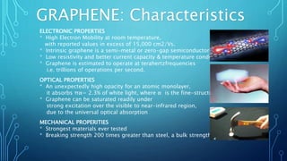


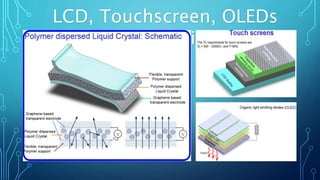
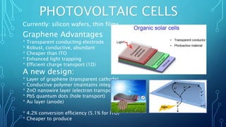


Graphene is a two-dimensional material composed of carbon atoms arranged in a hexagonal lattice. It has unique electrical, mechanical, and optical properties. In 2004, Geim and Novoselov developed the "scotch tape" method to isolate single-atom thick graphene sheets from graphite. This discovery led to the 2010 Nobel Prize in Physics. Graphene is synthesized through exfoliation of graphite or epitaxial growth on metal substrates. Potential future applications of graphene include use in biological engineering, optical electronics like touchscreens, ultrafiltration, photovoltaics, composite materials, and supercapacitors.


