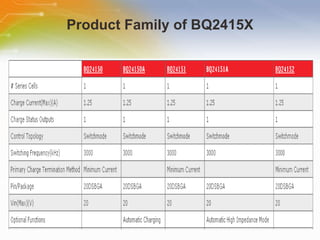
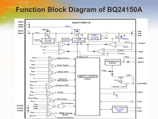
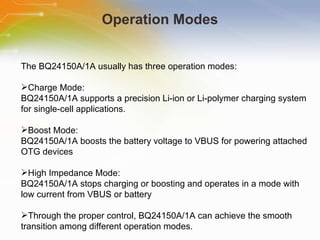
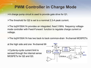
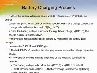
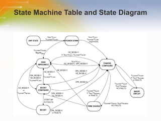
The document summarizes the features and operation of the Texas Instruments BQ2415X fully integrated single-cell Li-ion battery charger chip. Key features include high-efficiency charging, adjustable charge parameters via I2C interface, and a USB-friendly boot-up sequence. The chip operates in charge, boost, or high impedance modes and uses pulse-width modulation control during charging. It can charge common mobile device batteries and includes safety functions like current limiting and temperature protection.
Welcome to the training module on the fully integrated switch mode single cell Li-Ion charger BQ2415X. This training module introduces the block diagram, start up sequence and applications for the device.
The bq24150A/1A is a compact, flexible, high-efficiency, USB-friendly switch-mode charge management device for single-cell Li-ion and Li-polymer batteries used in a wide range of portable applications. The charge parameters can be programmed through an I2C interface. The bq2415X integrates a synchronous PWM controller, power MOSFETs, input current sensing, high-accuracy current and voltage regulation, and charge termination, into a small WCSP package.
Single-cell Li-ion and Li-polymer batteries are used in a wide range of portable applications like mobile and smart phones, MP3 player, Handheld devices Etc..
Here in this page Different families of BQ2415X device has been shown. BQ24150, BQ24150A, BQ24151, BQ24151A, BQ24152. BQ24151A has Automatic High Impedance Mode others do not have this feature.
I2C is a 2-wire serial interface developed by Philips Semiconductor. The bus consists of a data line (SDA) and a clock line (SCL) with pull-up structures. The master generates further SCL cycles to either transmit data to the slave (R/W bit 1) or receive data from the slave (R/W bit 0). In either case, the receiver needs to acknowledge the data sent by the transmitter. So an acknowledge signal can either be generated by the master or by the slave, depending on which one is the receiver. The 9-bit valid data sequences consisting of 8-bit data and 1-bit acknowledge can continue as long as necessary.
The bq24150A/1A is a highly integrated synchronous switch-mode charger with bi-directional operation to achieve boost function for USB OTG support, featuring integrated MOSFETs and small external components, targeted at extremely space-limited portable applications powered by 1-cell Li-Ion or Li-polymer battery pack. For a current limited power source, such as a USB host or hub, the high efficiency converter is critical in fully using the input power capacity and charging the battery. Due to the high efficiency in a wide range of the input voltage and battery voltage, the switching mode charger is a good choice for high speed charging with less power loss and better thermal management.
This page gives you typical characteristics of the device: During the charging process, the bq24150A/1A monitors its junction temperature (TJ) and reduces the charge current once TJ increases to approximately 125°C. To support USB OTG device, bq24150A/1A provides VBUS (approximately 5.05 V) by boosting the battery voltage.
The bq24150A/1A usually has three operation modes: charge mode, boost mode, and high impedance mode. In charge mode, the bq24150A/1A supports a precision Li-ion or Li-polymer charging system for single-cell applications. In boost mode, bq24150A/1A boosts the battery voltage to VBUS for powering attached OTG devices. In high impedance mode, the bq24150A/1A stops charging or boosting and operates in a mode with low current from VBUS or battery, to effectively reduce the power consumption when the portable device in standby mode. Through the proper control, bq24150A/1A can achieve the smooth transition among different operation modes.
The bq2415x integrates a synchronous PWM controller, power MOSFETs, input current sensing, high-accuracy current and voltage regulation, and charge termination, into a small WCSP package. The charge parameters can be programmed through an I2C interface. Cycle-by-cycle current limit is sensed through the internal sense MOSFETs for Q2 and Q3. The threshold for Q2 is set to a nominal 2.3-A peak current. The low-side MOSFET (Q3) also has a current limit that decides if the PWM Controller will operate in synchronous or non-synchronous mode.
At the beginning of precharge, while battery voltage is below the V(SHORT) threshold, the bq24150A/1A applies a short-circuit current, I(SHORT), to the battery. When the battery voltage is above V(SHORT) and below V(OREG), the charge current ramps up to fast charge current, IO(CHARGE), or a charge current that corresponds to the input current of I(IN_LIMIT). The slew rate for fast charge current is controlled to minimize the current and voltage over-shoot during transient. This device monitors the charging current during the voltage regulation phase. Once the termination threshold, ITERM, is detected and the battery voltage is above the recharge threshold, the device terminates charge.
Again, there are three operation modes: charge mode, boost mode, and high impedance mode along with state transitions form High impedance, Boost configure, Boost, PWM charge, Charge configure, Short circuit.
During normal charging process, the bq24150A/1A is normally in 32-second mode with host control, and 32-minute mode without host control using I2C interface. Boost mode enable control or input current limiting selection pin. When OTG is in active status, bq24150A/1A is forced to operate in boost mode. It has higher priority over I2C control and can be disabled through control register. The logic voltage level at OTG active status can also be controlled. At POR, the OTG pin is default to be used as the input current limiting selection pin. When OTG = High, Iin – limit = 500mA and when OTG = Low, Iin – limit = 100mA. If the battery voltage is below V(LOWV), but the host control using I2C interface is available (32 second mode), the device operates in a mode dictated by control registers.
This slides shows the BQ2415x Evaluation module which has High Efficiency Fully Integrated NMOS Synchronous Buck Charger With 3MHz Frequency, Integrated Power FETs for Up To 1.25-A Charge Rate, Programmable Battery Voltage, Charge Current, and Input Current via I2C Interface. Its Input Operating Range is 4 to 6V and it has Boost Mode Operation for USB OTG.
This is a typical application circuit for BQ2415X device used as pre-regulator application that operates as a DC/DC converter, with the termination disabled. the host charge controller controls switch Q to achieve pulse-charging function, and bq24150A/1A converts the input voltage to the lower output voltage (VOREG). The robust internal compensation design ensures the stable operation when the host-controlled switch Q is turned off.
Thank you for taking the time to view this presentation on “ BQ2415X” . If you would like to learn more or go on to purchase some of these devices, you may either click on the part list link, or simply call our sales hotline. For more technical information you may either visit the Texas Instrument site, or if you would prefer to speak to someone live, please call our hotline number, or even use our ‘live chat’ online facility. You may visit Element 14 e-community to post your questions.