Many different circuits have been devised to produce FM and PM signals.
There are two different types of frequency modulator circuits, direct circuits and circuits that produce FM indirectly by phase modulation techniques.
FM CIRCUITS
Many differentcircuits have been devised to produce FM and PM signals.
There are two different types of frequency modulator circuits, direct circuits and circuits that produce
FM indirectly by phase modulation techniques.
A- Direct FM circuits make use of techniques for varying the frequency of the carrier oscillator in
accordance with the modulating signal.
B- Indirect modulators produce FM via a phase shifter after the carrier oscillator stage.
Frequency demodulator or detector circuits convert the FM signal back to the original modulating
signal.
Most FM circuits today are inside integrated circuits, and some are implemented in software with
digital signal processing methods.
3.
6-1
FREQUENCY MODULATORS
A frequencymodulator is a circuit that varies carrier frequency in accordance with the modulating signal. The
carrier is generated by either an LC or a crystal oscillator circuit, and so a way must be found to change the
frequency of oscillation
In an LC oscillator, the carrier frequency is fixed by the values of the inductance and capacitance in a tuned circuit,
and the carrier frequency can therefore be changed by varying either inductance or capacitance. The idea is to find
a circuit or component that converts a modulating voltage to a corresponding change in capacitance or inductance
When the carrier is generated by a crystal oscillator, the frequency is fixed by the crystal. However, keep in mind
that the equivalent circuit of a crystal is an LCR circuit with both series and parallel resonant points. Connecting an
external capacitor to the crystal allows minor variations in operating frequency to be obtained. Again, the objective
is to find a circuit or component whose capacitance will change in response to the modulating signal
.
The component most frequently used for this purpose is a varactor. Also known as a voltage variable capacitor,
variable capacitance diode, or varicap, this device is basically a semiconductor junction diode operated in a
reverse-bias mode
.
4.
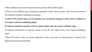
VARACTOR OPERATION
A junctiondiode is created when P- and N-type
semiconductors are formed during the manufacturing
process. Some electrons in the N-type material drift over
into the P-type material and neutralize the holes there
[see Fig], forming a thin area called the depletion region,
where there are no free carriers, holes, or electrons
.
This region acts as a thin insulator that prevents current
from l owing through the device. If a forward bias is
applied to the diode, it will conduct. The external
potential forces the holes and electrons toward the
junction, where they combine and cause a continuous
current inside the diode as well as externally
.
5.
The depletion layersimply
disappears [see Fig a. ]. If an
external reverse bias is applied to
the diode, as in Fig. b), no current
will low. The bias increases the
width of the depletion layer, with
the amount of increase depending
on the amount of the reverse bias.
The higher the reverse bias, the
wider the depletion layer and the
less chance for current l ow
.
The capacitance ofvaractor diode D1 and L1 forms the parallel-tuned circuit of the oscillator. The value of C1 is
made very large at the operating frequency so that its reactance is very low. As a result, C1 connects the tuned
circuit to the oscillator circuit
.
Also C1 blocks the dc bias on the base of Q1 from being shorted to ground through L1 . The values of L1 and
D1 fix the center carrier frequency. The capacitance of D1 is controlled in two ways, through a fixed dc bias and
by the modulating signal
.
In Fig. 6-4, the bias on D1 is set by the voltage divider potentiometer R4 . Varying R4 allows the center carrier
frequency to be adjusted over a narrow range
.
The modulating signal is applied through C5 and the radio frequency choke (RFC); C5 is a blocking capacitor
that keeps the dc varactor bias out of the modulating-signal circuits
.
The reactance of the RFC is high at the carrier frequency to prevent the carrier signal from getting back into the
audio modulating-signal circuits
.
9.
FREQUENCY-MODULATING A CRYSTALOSCILLATOR
It is possible to vary the frequency of a crystal
oscillator by changing the value of capacitance in
series or in parallel with the crystal
.
When a small value of capacitance is connected in
series with the crystal, the crystal frequency can be
“pulled” slightly from its natural resonant frequency
.
The modulating signal is applied to the varactor diode
D1 , which changes the oscillator frequency
.
10.
6-2
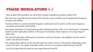
PHASE MODULATORS
Most modernFM transmitters use some form of phase modulation to produce indirect FM
.
The reason for using PM instead of direct FM is that the carrier oscillator can be optimized for frequency
accuracy and stability
.
Crystal oscillators or crystal-controlled frequency synthesizers can be used to set the carrier frequency
accurately and maintain solid stability
.
Some phase modulators are based upon the phase shift produced by an RC or LC tuned circuit. It should be
pointed out that simple phase shifters of this type do not produce linear response over a large range of
phase shift
.
The total allowable phase shift must be restricted to maximize linearity, and multipliers must be used to
achieve the desired deviation
.
The simplest phase shifters are RC networks like those shown in Fig. 6-10(a) and (b). Depending on the
values of R and C, the output of the phase shifter can be set to any phase angle between 0 and 90°
.
In (a), the output leads the input by some angle between 0 and 90°
.
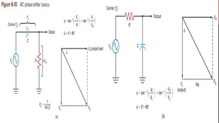
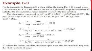
11.
For example, whenXc equals R, the phase shift is 45°. The phase shift is computed by using the formula
A low-pass RC filter can also be used, as shown in Fig. 6-10(b). Here the output is taken from across the
capacitor, so it lags the input voltage by some angle between 0 and 90°. The phase angle is computed by using
the formula
A simple phase-shift circuit can be used as a phase modulator if the resistance or capacitance can be made to
vary with the modulating signal. One way to do this is to replace the capacitor shown in the circuit of Fig. 6-
10(b) with a varactor
.
15.
6-3
FREQUENCY DEMODULATORS
Slope Detectors
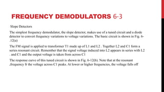
Thesimplest frequency demodulator, the slope detector, makes use of a tuned circuit and a diode
detector to convert frequency variations to voltage variations. The basic circuit is shown in Fig. 6-
12(a)
.
The FM signal is applied to transformer T1 made up of L1 and L2 . Together L2 and C1 form a
series resonant circuit. Remember that the signal voltage induced into L2 appears in series with L2
and C1 and the output voltage is taken from across C1
.
The response curve of this tuned circuit is shown in Fig. 6-12(b). Note that at the resonant
frequency fr the voltage across C1 peaks. At lower or higher frequencies, the voltage falls off
.
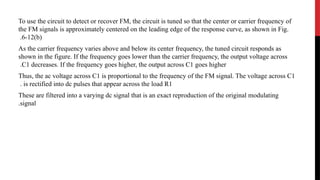
17.
To use thecircuit to detect or recover FM, the circuit is tuned so that the center or carrier frequency of
the FM signals is approximately centered on the leading edge of the response curve, as shown in Fig.
6-12(b)
.
As the carrier frequency varies above and below its center frequency, the tuned circuit responds as
shown in the figure. If the frequency goes lower than the carrier frequency, the output voltage across
C1 decreases. If the frequency goes higher, the output across C1 goes higher
.
Thus, the ac voltage across C1 is proportional to the frequency of the FM signal. The voltage across C1
is rectified into dc pulses that appear across the load R1
.
These are filtered into a varying dc signal that is an exact reproduction of the original modulating
signal
.
19.
QUADRATURE DETECTORS
The quadraturedetector uses a phase-shift circuit to produce a phase shift of 90° at the unmodulated carrier frequency.
The most commonly used phase-shift arrangement is shown in Fig. 6-15
.
The frequency-modulated signal is applied through a very small capacitor (C1 ) to the parallel-tuned circuit, which is
adjusted to resonate at the center carrier frequency
.
At resonance, the tuned circuit appears as a high value of pure resistance. The small capacitor has a very high
reactance compared to the tuned circuit impedance. Thus, the output across the tuned circuit at the carrier frequency is
very close to 90° and leads the input
20.
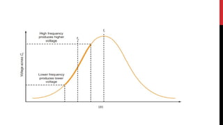
Fig. 6-16 showsthe typical waveforms involved in a quadrature detector. When there is no modulation,
the two input signals are exactly 90° out of phase and therefore provide an output pulse with the
indicated width
.
When the FM signal frequency increases, the amount of phase shift decreases, resulting in a wider
output pulse. The wider pulses averaged by the RC filter produce a higher average output voltage,
which corresponds to the higher amplitude required to produce the higher carrier frequency. When the
signal frequency decreases, greater phase shift and narrower output pulses occur
.
The narrower pulses, when averaged, produce a lower average output voltage, which corresponds to the
original lower-amplitude modulating signal
.
22.
When no inputsignal is applied, the phase detector and low-pass filter outputs are zero. The VCO then
operates at what is called the free-running frequency, its normal operating frequency as determined
by internal frequency-determining components
.
When an input signal close to the frequency of the VCO is applied, the phase detector compares the
VCO free-running frequency to the input frequency and produces an output voltage proportional to the
frequency difference
.
Most PLL phase detectors operate just as the one discussed in the section on quadrature detectors. The
phase detector output is a series of pulses that vary in width in accordance with the amount of phase
shift or frequency difference that exists between the two inputs. The output pulses are then filtered into
a dc voltage that is applied to the VCO. This dc voltage is such that it forces the VCO frequency to
move in a direction that reduces the dc error voltage
23.
Any variation ininput frequency is matched by a VCO frequency change, so the circuit remains
locked. The VCO in a PLL is, therefore, capable of tracking the input frequency over a wide range
.
The range of frequencies over which a PLL can track an input signal and remain locked is known as
the lock range. The lock range is usually a band of frequencies above and below the free-running
frequency of the VCO
.
If the input signal frequency is out of the lock range, the PLL will not lock. When this occurs, the
VCO output frequency jumps to its free-running frequency
.
If an input frequency within the lock range is applied to the PLL, the circuit immediately adjusts
itself into a locked condition
.
The phase detector determines the phase difference between the free-running and input frequencies
of the VCO and generates the error signal that forces the VCO to equal the input frequency
.
This action is referred to as capturing an input signal
24.
The range offrequencies over which a PLL will capture an input signal, known as the capture range, is
much narrower than the lock range, but, like the lock range, is generally centered on the free-running
frequency of the VCO (see Fig. 6-18)
25.
The characteristic thatcauses the PLL to capture signals within a certain frequency range causes it to act as a
bandpass filter
.
Phase-locked loops are often used in signal conditioning applications, where it is desirable to pass signals only in
a certain range and to reject signals outside of that range
.
The PLL is highly effective in eliminating the noise and interference on a signal
.
The ability of a PLL to provide frequency selectivity and filtering gives it a signal to-noise ratio superior to that of
any other type of FM detector
.
The linearity of the VCO ensures low distortion and a highly accurate reproduction of the original modulating
signal. Although PLLs are complex, they are easy to apply because they are readily available in low-cost IC form
.


![VARACTOR OPERATION
A junction diode is created when P- and N-type
semiconductors are formed during the manufacturing
process. Some electrons in the N-type material drift over
into the P-type material and neutralize the holes there
[see Fig], forming a thin area called the depletion region,
where there are no free carriers, holes, or electrons
.
This region acts as a thin insulator that prevents current
from l owing through the device. If a forward bias is
applied to the diode, it will conduct. The external
potential forces the holes and electrons toward the
junction, where they combine and cause a continuous
current inside the diode as well as externally
.](https://image.slidesharecdn.com/fmcircuits2-250515075907-9d9c3a59/85/FM-Circuits-Varactor-Modulators-2-pptx-4-320.jpg)
![The depletion layer simply
disappears [see Fig a. ]. If an
external reverse bias is applied to
the diode, as in Fig. b), no current
will low. The bias increases the
width of the depletion layer, with
the amount of increase depending
on the amount of the reverse bias.
The higher the reverse bias, the
wider the depletion layer and the
less chance for current l ow
.](https://image.slidesharecdn.com/fmcircuits2-250515075907-9d9c3a59/85/FM-Circuits-Varactor-Modulators-2-pptx-5-320.jpg)