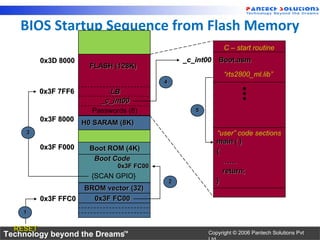
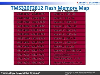
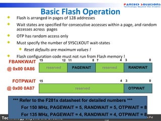
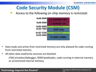
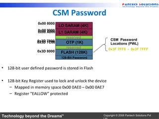
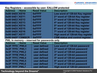
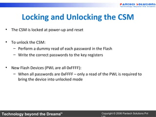
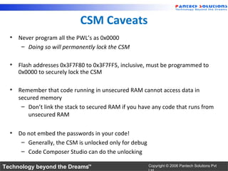
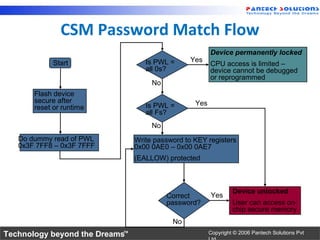
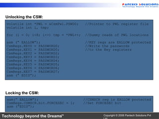
SlideShare a Scribd company logo
1 of 18
Chapter 10 : Flash
 Programming C28x


  Digital Signal Controller
    TMS320F2812


Technology beyond the Dreamsā„¢   Copyright Ā© 2006 Pantech Solutions Pvt
BIOS Startup Sequence from Flash Memory
                                                                C ā€“ start routine
          0x3D 8000                                _c_int00   Boot.asm
                        FLASH (128K)
                                                                ā€œrts2800_ml.libā€
                                           4
          0x3F 7FF6          LB
                          _c_int00
                        Passwords (8)                 5
          0x3F 8000   H0 SARAM (8K)
     3                                                        ā€œuserā€ code sections
                                                              main ( )
          0x3F F000    Boot ROM (4K)                          {
                        Boot Code                               ā€¦ā€¦
                               0x3F FC00
                                                                return;
                        {SCAN GPIO}
                                               2              }
                      BROM vector (32)
          0x3F FFC0     0x3F FC00
    1


  RESET
Technology beyond the Dreamsā„¢                             Copyright Ā© 2006 Pantech Solutions Pvt
TMS320F2812 Flash Memory Map
               Address Range          Data & Program Space
           0x3D 8000 ā€“ 0x3D 9FFF   Sector J ; 8K x 16
           0x3D A000 ā€“ 0x3D BFFF   Sector I ; 8K x 16
           0x3D C000 ā€“ 0x3D FFFF   Sector H : 16K x 16
           0x3E 0000 ā€“ 0x3E 3FFF   Sector G ; 16K x 16
           0x3E 4000 ā€“ 0x3E 7FFF   Sector F ; 16K x 16
           0x3E 8000 ā€“ 0x3E BFFF   Sector E ; 16K x 16
           0x3E C000 ā€“ 0x3E FFFF   Sector D; 16K x 16
           0x3F 0000 ā€“ 0x3F 3FFF   Sector C ; 16K x 16
           0x3F 4000 ā€“ 0x3F 5FFF   Sector B ; 8K x16
           0x3F 6000 ā€“ 0x3F 7F7F   Sector A ; (8K-128) x16
           0x3F 7F80 ā€“ 0x3F 7FF5   Program to 0x0000 when using
                                   Code Security Mode !
           0x3F 7FF6 ā€“ 0x3F 7FF7   Flash Entry Point ; 2 x 16
           0x3F 7FF8 ā€“ 0x3F 7FFF   Security Password ; 8 x 16


Technology beyond the Dreamsā„¢                  Copyright Ā© 2006 Pantech Solutions Pvt
Basic Flash Operation
  ļµ    Flash is arranged in pages of 128 addresses
  ļµ    Wait states are specified for consecutive accesses within a page, and random
       accesses across pages
  ļµ    OTP has random access only
  ļµ    Must specify the number of SYSCLKOUT wait-states
        ļµ   Reset defaults are maximum values !
  ļµ   Flash configuration code must not run from Flash memory !
                                                            4 3                    0
   FBANKWAIT 15                12 11           8 7

  @ 0x00 0A86            reserved    PAGEWAIT        reserved           RANDWAIT


      FOTPWAIT      15                                          4   3              0

  @ 0x00 0A87                          reserved                         OTPWAIT


      *** Refer to the F281x datasheet for detailed numbers ***
         For 150 MHz, PAGEWAIT = 5, RANDWAIT = 5, OTPWAIT = 8
         For 135 MHz, PAGEWAIT = 4, RANDWAIT = 4,Ā©OTPWAIT = 8 Pvt
Technology beyond the Dreamsā„¢             Copyright 2006 Pantech Solutions
Speeding Up Code Execution in
          16          Flash:
                    Flash Pipelining (for code fetch only)
                                                 16 or 32
                                      64         dispatched
                      64                                            C28x Core
                                                                    decoder unit
                    Aligned       2-level deep
                    64-bit        fetch buffer
                    fetch
                                                    Flash Pipeline Enable
                                                            0 = disable (default)
                                                            1 = enable


     FOPT @ 0x00 0A80
     15                                               1             0
                              reserved                         ENPIPE

Technology beyond the Dreamsā„¢                      Copyright Ā© 2006 Pantech Solutions Pvt
Other Flash Configuration Registers
       Address     Name              Description
       0x00 0A80   FOPT              Flash option register
       0x00 0A82   FPWR              Flash power modes registers
       0x00 0A83   FSTATUS           Flash status register
       0x00 0A84   FSTDBYWAIT        Flash sleep to standby wait register
       0x00 0A85   FACTIVEWAIT       Flash standby to active wait register
       0x00 0A86   FBANKWAIT         Flash read access wait state register
       0x00 0A87   FOTPWAIT          OTP read access wait state register
  ļµ    FPWR: Save power by putting Flash/OTP to ā€˜Sleepā€™ or ā€˜Standbyā€™
       mode; Flash will automatically enter active mode if a Flash/OTP
       access is made
  ļµ    FSTATUS: Various status bits (e.g. PWR mode)
  ļµ    FSTDBYWAIT: Specify number of cycles to wait during wake-up
       from sleep to standby
  ļµ    FACTIVEWAIT: Specify number of cycles to wait during wake-up
       from standby to active
  Defaults for these registers are often sufficient ā€“ See ā€œTMS320F28x DSP
  System Control and Interrupts Reference Guide,ā€ SPRU078, for more information

Technology beyond the Dreamsā„¢                         Copyright Ā© 2006 Pantech Solutions Pvt
Flash Programming Basics
ā€¢ The DSP CPU itself performs the flash programming
ā€¢ The CPU executes Flash utility code from RAM that reads the Flash data and writes it
  into the Flash
ā€¢ We need to get the Flash utility code and the Flash data into RAM


                                                                                   FLASH
                                                                                   FLASH
        Flash
        utility
        code                  Emulator        JTAG

                                 RS232         SCI


                                                                      Bootloader


                                                                                            F28x DSP
                                                                                            F28x DSP
        Flash


                                                              RAM
                                                              RAM


                                                                                   CPU
                                                                                   CPU
        Data                                    SPI


                                                                ROM
                                              GPIO


Technology beyond the Dreamsā„¢                                Copyright Ā© 2006 Pantech Solutions Pvt
ā€¢ Sequence of steps for Flash programming:
                  Algorithm         Function
             1. Erase         - Set all bits to zero, then to one
             2. Program       - Program selected bits with zero
             3. Verify        - Verify flash contents


 ā€¢ Minimum Erase size is a sector
 ā€¢ Minimum Program size is a bit!
 ā€¢ Important not to lose power during erase step: If CSM passwords happen to be
   all zeros, the CSM will be permanently locked!
 ā€¢ Chance of this happening is quite small! (Erase step is performed sector by
   sector)


Technology beyond the Dreamsā„¢                           Copyright Ā© 2006 Pantech Solutions Pvt
Flash Programming Utilities
 ā€¢ Code Composer Studio Plug-in (uses JTAG) *
 ā€¢ Serial Flash loader from TI (uses SCI boot) *
 ā€¢ Gang Programmers (use GPIO boot)
    ā€“ BP Micro programmer
    ā€“ Data I/O programmer
 ā€¢ Build your own custom utility
    ā€“ Use a different ROM bootloader method than SCI
    ā€“ Embed flash programming into your application
    ā€“ Flash API algorithms provided by TI


      * Available from TI web at www.ti.com
Technology beyond the Dreamsā„¢                     Copyright Ā© 2006 Pantech Solutions Pvt
Code Composer Studio
               Flash Plug-In


Technology beyond the Dreamsā„¢   Copyright Ā© 2006 Pantech Solutions Pvt
Code Security Module (CSM)
       ļµ    Access to the following on-chip memory is restricted:
                              0x00 8000
                                          LO SARAM (4K)
                              0x00 9000
                                          L1 SARAM (4K)
                              0x00 A000      reserved
                              0x3D 7800
                                             OTP (1K)
                             0x3D 7C00       reserved
                             0x3D 8000
                                           FLASH (128K)


ā€¢ Data reads and writes from restricted memory are only allowed for code running
  from restricted memory
ā€¢ All other data read/write accesses are blocked:
      JTAG emulator/debugger, ROM bootloader, code running in external memory
      or unrestricted internal memory


Technology beyond the Dreamsā„¢                           Copyright Ā© 2006 Pantech Solutions Pvt
CSM Password
                   0x00 8000
                               LO SARAM (4K)
                   0x00 9000
                   0x00 A000 L1 SARAM (4K)
                                 reserved
                   0x3D 7800                                 CSM Password
                   0x3D 7C00     OTP (1K)                    Locations (PWL)
                                 reserved                   0x3F 7FF8 - 0x3F 7FFF
                   0x3D 8000  FLASH (128K)
                                128-Bit Password


ā€¢ 128-bit user defined password is stored in Flash

ā€¢ 128-bit Key Register used to lock and unlock the device
   ā€“ Mapped in memory space 0x00 0AE0 ā€“ 0x00 0AE7
   ā€“ Register ā€œEALLOWā€ protected


Technology beyond the Dreamsā„¢                          Copyright Ā© 2006 Pantech Solutions Pvt
Key Registers ā€“ accessible by user; EALLOW protected
   Address    Name        Reset Value      Description
   0x00 0AE0 KEY0
   0x00 0AE1 KEY1     CSM Registers
                          0xFFFF
                          0xFFFF
                                           Low word of 128-bit Key register
                                           2nd word of 128-bit Key register
   0x00 0AE2 KEY2         0xFFFF           3rd word of 128-bit Key register
   0x00 0AE3 KEY3         0xFFFF           4th word of 128-bit Key register
   0x00 0AE4 KEY4         0xFFFF           5th word of 128-bit Key register
   0x00 0AE5 KEY5         0xFFFF           6th word of 128-bit Key register
   0x00 0AE6 KEY6         0xFFFF           7th word of 128-bit Key register
   0x00 0AE7 KEY7         0xFFFF           High word of 128-bit Key register
   0x00 0AEF CSMSCR 0xFFFF                 CSM status and control register
   PWL in memory ā€“ reserved for passwords only
   Address    Name        Reset Value       Description
   0x3F 7FF8 PWL0          user defined     Low word of 128-bit password
   0x3F 7FF9 PWL1          user defined     2nd word of 128-bit password
   0x3F 7FFA PWL2          user defined     3rd word of 128-bit password
   0x3F 7FFB PWL3          user defined     4th word of 128-bit password
   0x3F 7FFC PWL4          user defined     5th word of 128-bit password
   0x3F 7FFD PWL5          user defined     6th word of 128-bit password
   0x3F 7FFE PWL6          user defined     7th word of 128-bit password
   0x3F 7FFF PWL7         user defined      High word of 128-bit password
Technology beyond the Dreamsā„¢                      Copyright Ā© 2006 Pantech Solutions Pvt
Locking and Unlocking the CSM
 ā€¢ The CSM is locked at power-up and reset

 ā€¢ To unlock the CSM:
    ā€“ Perform a dummy read of each password in the Flash
    ā€“ Write the correct passwords to the key registers

 ā€¢ New Flash Devices (PWL are all 0xFFFF):
    ā€“ When all passwords are 0xFFFF ā€“ only a read of the PWL is required to
      bring the device into unlocked mode


Technology beyond the Dreamsā„¢                        Copyright Ā© 2006 Pantech Solutions Pvt
CSM Caveats
  ā€¢ Never program all the PWLā€™s as 0x0000
     ā€“ Doing so will permanently lock the CSM

  ā€¢ Flash addresses 0x3F7F80 to 0x3F7FF5, inclusive, must be programmed to
    0x0000 to securely lock the CSM

  ā€¢ Remember that code running in unsecured RAM cannot access data in
    secured memory
     ā€“ Donā€™t link the stack to secured RAM if you have any code that runs from
        unsecured RAM

  ā€¢ Do not embed the passwords in your code!
     ā€“ Generally, the CSM is unlocked only for debug
     ā€“ Code Composer Studio can do the unlocking

Technology beyond the Dreamsā„¢                          Copyright Ā© 2006 Pantech Solutions Pvt
CSM Password Match Flow
                                                        Device permanently locked
             Start                 Is PWL =      Yes
                                                        CPU access is limited ā€“
                                   all 0s?              device cannot be debugged
                                                        or reprogrammed
                                     No
       Flash device
       secure after                               Yes
       reset or runtime            Is PWL =
                                   all Fs?
                                     No
   Do dummy read of PWL         Write password to KEY registers
   0x3F 7FF8 ā€“ 0x3F 7FFF        0x00 0AE0 ā€“ 0x00 0AE7
                                (EALLOW) protected


                                                                 Device unlocked
                                          Correct       Yes
                                          password?              User can access on-
                                                                 chip secure memory
                                           No
Technology beyond the Dreamsā„¢                           Copyright Ā© 2006 Pantech Solutions Pvt
Unlocking the CSM:

           CSM C-Code Examples
  volatile int *PWL = &CsmPwl.PSWD0;
  volatile int i, tmp;
                                        //Pointer to PWL register file


  for (i = 0; i<8; i++) tmp = *PWL++;   //Dummy reads of PWL locations

  asm (ā€ EALLOWā€);                      //KEY regs are EALLOW protected
  CsmRegs.KEY0 = PASSWORD0;             //Write the passwords
  CsmRegs.KEY1 = PASSWORD0;             //to the Key registers
  CsmRegs.KEY2 = PASSWORD2;
  CsmRegs.KEY3 = PASSWORD3;
  CsmRegs.KEY4 = PASSWORD4;
  CsmRegs.KEY5 = PASSWORD5;
  CsmRegs.KEY6 = PASSWORD6;
  CsmRegs.KEY7 = PASSWORD7;
  asm (ā€ EDISā€);


 Locking the CSM:
  asm(ā€ EALLOWā€);                       //CSMSCR reg is EALLOW protected
  CsmRegs.CSMSCR.bit.FORCESEC = 1;      //Set FORCESEC bit
  asm (ā€EDISā€);

Technology beyond the Dreamsā„¢                    Copyright Ā© 2006 Pantech Solutions Pvt
Lab 11: Load an application into Flash
       ļ·   Use Solution for Lab4 to begin with
       ļ·   Modify the project to use internal Flash for code
       ļ·   Add ā€œDSP281x_CodeStartBranch.asmā€ to branch from Flash entry point
           ( 0x3F 7FF6) to C - library function ā€œ_c_int00ā€
       ļ·   Add TI - code to set up the speed of Flash
       ļ·   Add a function to move the speed-up code from Flash to SARAM Adjust
           Linker Command File
       ļ·   Use CCS plug-in tool to perform the Flash download
       ļ·   Disconnect emulator, set eZdsp into MC-mode (JP1) and re-power the
           board!
       ļ·   Code should be executed out of Flash
       ļ·   For details see procedure in textbook!


Technology beyond the Dreamsā„¢                        Copyright Ā© 2006 Pantech Solutions Pvt

More Related Content

What's hot

GPS-320FW
GPS-320FWGPS-320FW
GPS-320FWenenxx
Ā 
Message Signaled Interrupts
Message Signaled InterruptsMessage Signaled Interrupts
Message Signaled InterruptsAnshuman Biswal
Ā 
GGM8000-FIPs-Certification
GGM8000-FIPs-CertificationGGM8000-FIPs-Certification
GGM8000-FIPs-CertificationDavid Kiefer
Ā 
QPACE QCD Parallel Computing on the Cell Broadband Engineā„¢ (Cell/B.E.)
QPACE QCD Parallel Computing on the Cell Broadband Engineā„¢ (Cell/B.E.)QPACE QCD Parallel Computing on the Cell Broadband Engineā„¢ (Cell/B.E.)
QPACE QCD Parallel Computing on the Cell Broadband Engineā„¢ (Cell/B.E.)Heiko Joerg Schick
Ā 
Blueoptics bo56jxx660d 10gbase cwdm sfp+ transceiver 60km singlemode lc duple...
Blueoptics bo56jxx660d 10gbase cwdm sfp+ transceiver 60km singlemode lc duple...Blueoptics bo56jxx660d 10gbase cwdm sfp+ transceiver 60km singlemode lc duple...
Blueoptics bo56jxx660d 10gbase cwdm sfp+ transceiver 60km singlemode lc duple...CBO GmbH
Ā 
Webinar: Wearables - Apresentando um diagrama de blocos e componentes chaves
Webinar: Wearables - Apresentando um diagrama de blocos e componentes chavesWebinar: Wearables - Apresentando um diagrama de blocos e componentes chaves
Webinar: Wearables - Apresentando um diagrama de blocos e componentes chavesEmbarcados
Ā 
Altera Cyclone IV FPGA Customer Presentation
Altera Cyclone IV FPGA Customer PresentationAltera Cyclone IV FPGA Customer Presentation
Altera Cyclone IV FPGA Customer PresentationAltera Corporation
Ā 
MYS-6ULX Single Board Computer for Industry 4.0 and IoT Applications
MYS-6ULX Single Board Computer for Industry 4.0 and IoT ApplicationsMYS-6ULX Single Board Computer for Industry 4.0 and IoT Applications
MYS-6ULX Single Board Computer for Industry 4.0 and IoT ApplicationsLinda Zhang
Ā 
Technical s7889
Technical s7889Technical s7889
Technical s7889huslen_du
Ā 
xbee pro digi-mesh 2.4 oem rf modules
xbee pro  digi-mesh  2.4 oem rf modulesxbee pro  digi-mesh  2.4 oem rf modules
xbee pro digi-mesh 2.4 oem rf modulesSyamim Sempoi
Ā 
Np unit iv i
Np unit iv iNp unit iv i
Np unit iv ivamsitricks
Ā 
selfridge_alec_chipspec
selfridge_alec_chipspecselfridge_alec_chipspec
selfridge_alec_chipspecAlec Selfridge
Ā 
Sevana Voice Impairments Detection Library
Sevana Voice Impairments Detection LibrarySevana Voice Impairments Detection Library
Sevana Voice Impairments Detection LibrarySevana OĆ¼
Ā 
Adv. FPGA Motor Control--EBV & Univ. of Koln: Embedded World 2010
Adv. FPGA Motor Control--EBV & Univ. of Koln: Embedded World 2010Adv. FPGA Motor Control--EBV & Univ. of Koln: Embedded World 2010
Adv. FPGA Motor Control--EBV & Univ. of Koln: Embedded World 2010Altera Corporation
Ā 
Continuum PCAP
Continuum PCAP Continuum PCAP
Continuum PCAP rwachsman
Ā 
Blueoptics bo56hxx610d 8gbase-cwdm sfp+ transceiver 10km singlemode lc duplex...
Blueoptics bo56hxx610d 8gbase-cwdm sfp+ transceiver 10km singlemode lc duplex...Blueoptics bo56hxx610d 8gbase-cwdm sfp+ transceiver 10km singlemode lc duplex...
Blueoptics bo56hxx610d 8gbase-cwdm sfp+ transceiver 10km singlemode lc duplex...CBO GmbH
Ā 

What's hot (20)

Pic base a_1
Pic base a_1Pic base a_1
Pic base a_1
Ā 
LINUX RS232ē؋式čØ­č؈
LINUX RS232ē؋式čØ­č؈LINUX RS232ē؋式čØ­č؈
LINUX RS232ē؋式čØ­č؈
Ā 
GPS-320FW
GPS-320FWGPS-320FW
GPS-320FW
Ā 
Message Signaled Interrupts
Message Signaled InterruptsMessage Signaled Interrupts
Message Signaled Interrupts
Ā 
GGM8000-FIPs-Certification
GGM8000-FIPs-CertificationGGM8000-FIPs-Certification
GGM8000-FIPs-Certification
Ā 
QPACE QCD Parallel Computing on the Cell Broadband Engineā„¢ (Cell/B.E.)
QPACE QCD Parallel Computing on the Cell Broadband Engineā„¢ (Cell/B.E.)QPACE QCD Parallel Computing on the Cell Broadband Engineā„¢ (Cell/B.E.)
QPACE QCD Parallel Computing on the Cell Broadband Engineā„¢ (Cell/B.E.)
Ā 
Blueoptics bo56jxx660d 10gbase cwdm sfp+ transceiver 60km singlemode lc duple...
Blueoptics bo56jxx660d 10gbase cwdm sfp+ transceiver 60km singlemode lc duple...Blueoptics bo56jxx660d 10gbase cwdm sfp+ transceiver 60km singlemode lc duple...
Blueoptics bo56jxx660d 10gbase cwdm sfp+ transceiver 60km singlemode lc duple...
Ā 
Webinar: Wearables - Apresentando um diagrama de blocos e componentes chaves
Webinar: Wearables - Apresentando um diagrama de blocos e componentes chavesWebinar: Wearables - Apresentando um diagrama de blocos e componentes chaves
Webinar: Wearables - Apresentando um diagrama de blocos e componentes chaves
Ā 
Altera Cyclone IV FPGA Customer Presentation
Altera Cyclone IV FPGA Customer PresentationAltera Cyclone IV FPGA Customer Presentation
Altera Cyclone IV FPGA Customer Presentation
Ā 
MYS-6ULX Single Board Computer for Industry 4.0 and IoT Applications
MYS-6ULX Single Board Computer for Industry 4.0 and IoT ApplicationsMYS-6ULX Single Board Computer for Industry 4.0 and IoT Applications
MYS-6ULX Single Board Computer for Industry 4.0 and IoT Applications
Ā 
Ks 868 e-users_manual of home security devices
Ks 868 e-users_manual of home security devicesKs 868 e-users_manual of home security devices
Ks 868 e-users_manual of home security devices
Ā 
Technical s7889
Technical s7889Technical s7889
Technical s7889
Ā 
xbee pro digi-mesh 2.4 oem rf modules
xbee pro  digi-mesh  2.4 oem rf modulesxbee pro  digi-mesh  2.4 oem rf modules
xbee pro digi-mesh 2.4 oem rf modules
Ā 
Np unit iv i
Np unit iv iNp unit iv i
Np unit iv i
Ā 
selfridge_alec_chipspec
selfridge_alec_chipspecselfridge_alec_chipspec
selfridge_alec_chipspec
Ā 
Chapter 2.doc
Chapter 2.docChapter 2.doc
Chapter 2.doc
Ā 
Sevana Voice Impairments Detection Library
Sevana Voice Impairments Detection LibrarySevana Voice Impairments Detection Library
Sevana Voice Impairments Detection Library
Ā 
Adv. FPGA Motor Control--EBV & Univ. of Koln: Embedded World 2010
Adv. FPGA Motor Control--EBV & Univ. of Koln: Embedded World 2010Adv. FPGA Motor Control--EBV & Univ. of Koln: Embedded World 2010
Adv. FPGA Motor Control--EBV & Univ. of Koln: Embedded World 2010
Ā 
Continuum PCAP
Continuum PCAP Continuum PCAP
Continuum PCAP
Ā 
Blueoptics bo56hxx610d 8gbase-cwdm sfp+ transceiver 10km singlemode lc duplex...
Blueoptics bo56hxx610d 8gbase-cwdm sfp+ transceiver 10km singlemode lc duplex...Blueoptics bo56hxx610d 8gbase-cwdm sfp+ transceiver 10km singlemode lc duplex...
Blueoptics bo56hxx610d 8gbase-cwdm sfp+ transceiver 10km singlemode lc duplex...
Ā 

Similar to Flash Programming F28x

At 89s51
At 89s51At 89s51
At 89s51Mr Giap
Ā 
Microprocessor vs. microcontroller
Microprocessor vs. microcontrollerMicroprocessor vs. microcontroller
Microprocessor vs. microcontrolleraviban
Ā 
Robotix Tutorial 9
Robotix Tutorial 9Robotix Tutorial 9
Robotix Tutorial 9ankuredkie
Ā 
The hardware of the Mcs 51 microcontroller
 The hardware of the Mcs 51 microcontroller The hardware of the Mcs 51 microcontroller
The hardware of the Mcs 51 microcontrollerGarba Geidam
Ā 
An Overview of Arm-9 32-bit MCU TMPA910 Series
An Overview of Arm-9 32-bit MCU TMPA910 Series An Overview of Arm-9 32-bit MCU TMPA910 Series
An Overview of Arm-9 32-bit MCU TMPA910 Series Premier Farnell
Ā 
8086 microprocessor
8086 microprocessor8086 microprocessor
8086 microprocessorsavitamhaske
Ā 
An Overview Study on 32-bit MCU MB91460 Series and its Peripherals
An Overview Study on 32-bit MCU MB91460 Series and its PeripheralsAn Overview Study on 32-bit MCU MB91460 Series and its Peripherals
An Overview Study on 32-bit MCU MB91460 Series and its PeripheralsPremier Farnell
Ā 
Assembly programming
Assembly programmingAssembly programming
Assembly programmingOmar Sanchez
Ā 
A 32-Bit Parameterized Leon-3 Processor with Custom Peripheral Integration
A 32-Bit Parameterized Leon-3 Processor with Custom Peripheral IntegrationA 32-Bit Parameterized Leon-3 Processor with Custom Peripheral Integration
A 32-Bit Parameterized Leon-3 Processor with Custom Peripheral IntegrationTalal Khaliq
Ā 
Chp4 introduction to the pic microcontroller copy
Chp4 introduction to the pic microcontroller   copyChp4 introduction to the pic microcontroller   copy
Chp4 introduction to the pic microcontroller copymkazree
Ā 
SYBSC IT SEM IV EMBEDDED SYSTEMS UNIT II Processor Family
SYBSC IT SEM IV EMBEDDED SYSTEMS UNIT II Processor FamilySYBSC IT SEM IV EMBEDDED SYSTEMS UNIT II Processor Family
SYBSC IT SEM IV EMBEDDED SYSTEMS UNIT II Processor FamilyArti Parab Academics
Ā 

Similar to Flash Programming F28x (20)

At 89s51
At 89s51At 89s51
At 89s51
Ā 
Microprocessor vs. microcontroller
Microprocessor vs. microcontrollerMicroprocessor vs. microcontroller
Microprocessor vs. microcontroller
Ā 
At89s51
At89s51At89s51
At89s51
Ā 
datasheet.pdf
datasheet.pdfdatasheet.pdf
datasheet.pdf
Ā 
Datasheet
DatasheetDatasheet
Datasheet
Ā 
Robotix Tutorial 9
Robotix Tutorial 9Robotix Tutorial 9
Robotix Tutorial 9
Ā 
The hardware of the Mcs 51 microcontroller
 The hardware of the Mcs 51 microcontroller The hardware of the Mcs 51 microcontroller
The hardware of the Mcs 51 microcontroller
Ā 
8086
80868086
8086
Ā 
unit-2.pptx
unit-2.pptxunit-2.pptx
unit-2.pptx
Ā 
One day-workshop on tms320 f2812
One day-workshop on tms320 f2812One day-workshop on tms320 f2812
One day-workshop on tms320 f2812
Ā 
Microcontroller at89 s52 datasheet
Microcontroller at89 s52 datasheetMicrocontroller at89 s52 datasheet
Microcontroller at89 s52 datasheet
Ā 
An Overview of Arm-9 32-bit MCU TMPA910 Series
An Overview of Arm-9 32-bit MCU TMPA910 Series An Overview of Arm-9 32-bit MCU TMPA910 Series
An Overview of Arm-9 32-bit MCU TMPA910 Series
Ā 
8086 microprocessor
8086 microprocessor8086 microprocessor
8086 microprocessor
Ā 
Getting started with pic microcontrollers
Getting started with pic microcontrollersGetting started with pic microcontrollers
Getting started with pic microcontrollers
Ā 
An Overview Study on 32-bit MCU MB91460 Series and its Peripherals
An Overview Study on 32-bit MCU MB91460 Series and its PeripheralsAn Overview Study on 32-bit MCU MB91460 Series and its Peripherals
An Overview Study on 32-bit MCU MB91460 Series and its Peripherals
Ā 
Assembly programming
Assembly programmingAssembly programming
Assembly programming
Ā 
A 32-Bit Parameterized Leon-3 Processor with Custom Peripheral Integration
A 32-Bit Parameterized Leon-3 Processor with Custom Peripheral IntegrationA 32-Bit Parameterized Leon-3 Processor with Custom Peripheral Integration
A 32-Bit Parameterized Leon-3 Processor with Custom Peripheral Integration
Ā 
Tms320F2812 Digital I/0
Tms320F2812 Digital I/0Tms320F2812 Digital I/0
Tms320F2812 Digital I/0
Ā 
Chp4 introduction to the pic microcontroller copy
Chp4 introduction to the pic microcontroller   copyChp4 introduction to the pic microcontroller   copy
Chp4 introduction to the pic microcontroller copy
Ā 
SYBSC IT SEM IV EMBEDDED SYSTEMS UNIT II Processor Family
SYBSC IT SEM IV EMBEDDED SYSTEMS UNIT II Processor FamilySYBSC IT SEM IV EMBEDDED SYSTEMS UNIT II Processor Family
SYBSC IT SEM IV EMBEDDED SYSTEMS UNIT II Processor Family
Ā 

More from Pantech ProLabs India Pvt Ltd

Choosing the right processor for embedded system design
Choosing the right processor for embedded system designChoosing the right processor for embedded system design
Choosing the right processor for embedded system designPantech ProLabs India Pvt Ltd
Ā 
Median filter Implementation using TMS320C6745
Median filter Implementation using TMS320C6745Median filter Implementation using TMS320C6745
Median filter Implementation using TMS320C6745Pantech ProLabs India Pvt Ltd
Ā 

More from Pantech ProLabs India Pvt Ltd (20)

Registration process
Registration processRegistration process
Registration process
Ā 
Choosing the right processor for embedded system design
Choosing the right processor for embedded system designChoosing the right processor for embedded system design
Choosing the right processor for embedded system design
Ā 
Brain Computer Interface
Brain Computer InterfaceBrain Computer Interface
Brain Computer Interface
Ā 
Electric Vehicle Design using Matlab
Electric Vehicle Design using MatlabElectric Vehicle Design using Matlab
Electric Vehicle Design using Matlab
Ā 
Image processing application
Image processing applicationImage processing application
Image processing application
Ā 
Internet of Things using Raspberry Pi
Internet of Things using Raspberry PiInternet of Things using Raspberry Pi
Internet of Things using Raspberry Pi
Ā 
Internet of Things Using Arduino
Internet of Things Using ArduinoInternet of Things Using Arduino
Internet of Things Using Arduino
Ā 
Brain controlled robot
Brain controlled robotBrain controlled robot
Brain controlled robot
Ā 
Brain Computer Interface-Webinar
Brain Computer Interface-WebinarBrain Computer Interface-Webinar
Brain Computer Interface-Webinar
Ā 
Development of Deep Learning Architecture
Development of Deep Learning ArchitectureDevelopment of Deep Learning Architecture
Development of Deep Learning Architecture
Ā 
Future of AI
Future of AIFuture of AI
Future of AI
Ā 
Gate driver design and inductance fabrication
Gate driver design and inductance fabricationGate driver design and inductance fabrication
Gate driver design and inductance fabrication
Ā 
Brainsense -Brain computer Interface
Brainsense -Brain computer InterfaceBrainsense -Brain computer Interface
Brainsense -Brain computer Interface
Ā 
Median filter Implementation using TMS320C6745
Median filter Implementation using TMS320C6745Median filter Implementation using TMS320C6745
Median filter Implementation using TMS320C6745
Ā 
Introduction to Code Composer Studio 4
Introduction to Code Composer Studio 4Introduction to Code Composer Studio 4
Introduction to Code Composer Studio 4
Ā 
Waveform Generation Using TMS320C6745 DSP
Waveform Generation Using TMS320C6745 DSPWaveform Generation Using TMS320C6745 DSP
Waveform Generation Using TMS320C6745 DSP
Ā 
Interfacing UART with tms320C6745
Interfacing UART with tms320C6745Interfacing UART with tms320C6745
Interfacing UART with tms320C6745
Ā 
Switch & LED using TMS320C6745 DSP
Switch & LED using TMS320C6745 DSPSwitch & LED using TMS320C6745 DSP
Switch & LED using TMS320C6745 DSP
Ā 
Led blinking using TMS320C6745
Led blinking using TMS320C6745Led blinking using TMS320C6745
Led blinking using TMS320C6745
Ā 
Introduction to tms320c6745 dsp
Introduction to tms320c6745 dspIntroduction to tms320c6745 dsp
Introduction to tms320c6745 dsp
Ā 

Recently uploaded

ECONOMIC CONTEXT - LONG FORM TV DRAMA - PPT
ECONOMIC CONTEXT - LONG FORM TV DRAMA - PPTECONOMIC CONTEXT - LONG FORM TV DRAMA - PPT
ECONOMIC CONTEXT - LONG FORM TV DRAMA - PPTiammrhaywood
Ā 
Introduction to AI in Higher Education_draft.pptx
Introduction to AI in Higher Education_draft.pptxIntroduction to AI in Higher Education_draft.pptx
Introduction to AI in Higher Education_draft.pptxpboyjonauth
Ā 
Class 11 Legal Studies Ch-1 Concept of State .pdf
Class 11 Legal Studies Ch-1 Concept of State .pdfClass 11 Legal Studies Ch-1 Concept of State .pdf
Class 11 Legal Studies Ch-1 Concept of State .pdfakmcokerachita
Ā 
Hybridoma Technology ( Production , Purification , and Application )
Hybridoma Technology  ( Production , Purification , and Application  ) Hybridoma Technology  ( Production , Purification , and Application  )
Hybridoma Technology ( Production , Purification , and Application ) Sakshi Ghasle
Ā 
History Class XII Ch. 3 Kinship, Caste and Class (1).pptx
History Class XII Ch. 3 Kinship, Caste and Class (1).pptxHistory Class XII Ch. 3 Kinship, Caste and Class (1).pptx
History Class XII Ch. 3 Kinship, Caste and Class (1).pptxsocialsciencegdgrohi
Ā 
A Critique of the Proposed National Education Policy Reform
A Critique of the Proposed National Education Policy ReformA Critique of the Proposed National Education Policy Reform
A Critique of the Proposed National Education Policy ReformChameera Dedduwage
Ā 
How to Make a Pirate ship Primary Education.pptx
How to Make a Pirate ship Primary Education.pptxHow to Make a Pirate ship Primary Education.pptx
How to Make a Pirate ship Primary Education.pptxmanuelaromero2013
Ā 
Incoming and Outgoing Shipments in 1 STEP Using Odoo 17
Incoming and Outgoing Shipments in 1 STEP Using Odoo 17Incoming and Outgoing Shipments in 1 STEP Using Odoo 17
Incoming and Outgoing Shipments in 1 STEP Using Odoo 17Celine George
Ā 
Biting mechanism of poisonous snakes.pdf
Biting mechanism of poisonous snakes.pdfBiting mechanism of poisonous snakes.pdf
Biting mechanism of poisonous snakes.pdfadityarao40181
Ā 
ENGLISH5 QUARTER4 MODULE1 WEEK1-3 How Visual and Multimedia Elements.pptx
ENGLISH5 QUARTER4 MODULE1 WEEK1-3 How Visual and Multimedia Elements.pptxENGLISH5 QUARTER4 MODULE1 WEEK1-3 How Visual and Multimedia Elements.pptx
ENGLISH5 QUARTER4 MODULE1 WEEK1-3 How Visual and Multimedia Elements.pptxAnaBeatriceAblay2
Ā 
Painted Grey Ware.pptx, PGW Culture of India
Painted Grey Ware.pptx, PGW Culture of IndiaPainted Grey Ware.pptx, PGW Culture of India
Painted Grey Ware.pptx, PGW Culture of IndiaVirag Sontakke
Ā 
EPANDING THE CONTENT OF AN OUTLINE using notes.pptx
EPANDING THE CONTENT OF AN OUTLINE using notes.pptxEPANDING THE CONTENT OF AN OUTLINE using notes.pptx
EPANDING THE CONTENT OF AN OUTLINE using notes.pptxRaymartEstabillo3
Ā 
BASLIQ CURRENT LOOKBOOK LOOKBOOK(1) (1).pdf
BASLIQ CURRENT LOOKBOOK  LOOKBOOK(1) (1).pdfBASLIQ CURRENT LOOKBOOK  LOOKBOOK(1) (1).pdf
BASLIQ CURRENT LOOKBOOK LOOKBOOK(1) (1).pdfSoniaTolstoy
Ā 
Sanyam Choudhary Chemistry practical.pdf
Sanyam Choudhary Chemistry practical.pdfSanyam Choudhary Chemistry practical.pdf
Sanyam Choudhary Chemistry practical.pdfsanyamsingh5019
Ā 
Blooming Together_ Growing a Community Garden Worksheet.docx
Blooming Together_ Growing a Community Garden Worksheet.docxBlooming Together_ Growing a Community Garden Worksheet.docx
Blooming Together_ Growing a Community Garden Worksheet.docxUnboundStockton
Ā 
POINT- BIOCHEMISTRY SEM 2 ENZYMES UNIT 5.pptx
POINT- BIOCHEMISTRY SEM 2 ENZYMES UNIT 5.pptxPOINT- BIOCHEMISTRY SEM 2 ENZYMES UNIT 5.pptx
POINT- BIOCHEMISTRY SEM 2 ENZYMES UNIT 5.pptxSayali Powar
Ā 
Call Girls in Dwarka Mor Delhi Contact Us 9654467111
Call Girls in Dwarka Mor Delhi Contact Us 9654467111Call Girls in Dwarka Mor Delhi Contact Us 9654467111
Call Girls in Dwarka Mor Delhi Contact Us 9654467111Sapana Sha
Ā 
CARE OF CHILD IN INCUBATOR..........pptx
CARE OF CHILD IN INCUBATOR..........pptxCARE OF CHILD IN INCUBATOR..........pptx
CARE OF CHILD IN INCUBATOR..........pptxGaneshChakor2
Ā 

Recently uploaded (20)

ECONOMIC CONTEXT - LONG FORM TV DRAMA - PPT
ECONOMIC CONTEXT - LONG FORM TV DRAMA - PPTECONOMIC CONTEXT - LONG FORM TV DRAMA - PPT
ECONOMIC CONTEXT - LONG FORM TV DRAMA - PPT
Ā 
Introduction to AI in Higher Education_draft.pptx
Introduction to AI in Higher Education_draft.pptxIntroduction to AI in Higher Education_draft.pptx
Introduction to AI in Higher Education_draft.pptx
Ā 
Class 11 Legal Studies Ch-1 Concept of State .pdf
Class 11 Legal Studies Ch-1 Concept of State .pdfClass 11 Legal Studies Ch-1 Concept of State .pdf
Class 11 Legal Studies Ch-1 Concept of State .pdf
Ā 
Hybridoma Technology ( Production , Purification , and Application )
Hybridoma Technology  ( Production , Purification , and Application  ) Hybridoma Technology  ( Production , Purification , and Application  )
Hybridoma Technology ( Production , Purification , and Application )
Ā 
History Class XII Ch. 3 Kinship, Caste and Class (1).pptx
History Class XII Ch. 3 Kinship, Caste and Class (1).pptxHistory Class XII Ch. 3 Kinship, Caste and Class (1).pptx
History Class XII Ch. 3 Kinship, Caste and Class (1).pptx
Ā 
A Critique of the Proposed National Education Policy Reform
A Critique of the Proposed National Education Policy ReformA Critique of the Proposed National Education Policy Reform
A Critique of the Proposed National Education Policy Reform
Ā 
How to Make a Pirate ship Primary Education.pptx
How to Make a Pirate ship Primary Education.pptxHow to Make a Pirate ship Primary Education.pptx
How to Make a Pirate ship Primary Education.pptx
Ā 
Incoming and Outgoing Shipments in 1 STEP Using Odoo 17
Incoming and Outgoing Shipments in 1 STEP Using Odoo 17Incoming and Outgoing Shipments in 1 STEP Using Odoo 17
Incoming and Outgoing Shipments in 1 STEP Using Odoo 17
Ā 
Biting mechanism of poisonous snakes.pdf
Biting mechanism of poisonous snakes.pdfBiting mechanism of poisonous snakes.pdf
Biting mechanism of poisonous snakes.pdf
Ā 
ENGLISH5 QUARTER4 MODULE1 WEEK1-3 How Visual and Multimedia Elements.pptx
ENGLISH5 QUARTER4 MODULE1 WEEK1-3 How Visual and Multimedia Elements.pptxENGLISH5 QUARTER4 MODULE1 WEEK1-3 How Visual and Multimedia Elements.pptx
ENGLISH5 QUARTER4 MODULE1 WEEK1-3 How Visual and Multimedia Elements.pptx
Ā 
Painted Grey Ware.pptx, PGW Culture of India
Painted Grey Ware.pptx, PGW Culture of IndiaPainted Grey Ware.pptx, PGW Culture of India
Painted Grey Ware.pptx, PGW Culture of India
Ā 
EPANDING THE CONTENT OF AN OUTLINE using notes.pptx
EPANDING THE CONTENT OF AN OUTLINE using notes.pptxEPANDING THE CONTENT OF AN OUTLINE using notes.pptx
EPANDING THE CONTENT OF AN OUTLINE using notes.pptx
Ā 
9953330565 Low Rate Call Girls In Rohini Delhi NCR
9953330565 Low Rate Call Girls In Rohini  Delhi NCR9953330565 Low Rate Call Girls In Rohini  Delhi NCR
9953330565 Low Rate Call Girls In Rohini Delhi NCR
Ā 
Model Call Girl in Bikash Puri Delhi reach out to us at šŸ”9953056974šŸ”
Model Call Girl in Bikash Puri  Delhi reach out to us at šŸ”9953056974šŸ”Model Call Girl in Bikash Puri  Delhi reach out to us at šŸ”9953056974šŸ”
Model Call Girl in Bikash Puri Delhi reach out to us at šŸ”9953056974šŸ”
Ā 
BASLIQ CURRENT LOOKBOOK LOOKBOOK(1) (1).pdf
BASLIQ CURRENT LOOKBOOK  LOOKBOOK(1) (1).pdfBASLIQ CURRENT LOOKBOOK  LOOKBOOK(1) (1).pdf
BASLIQ CURRENT LOOKBOOK LOOKBOOK(1) (1).pdf
Ā 
Sanyam Choudhary Chemistry practical.pdf
Sanyam Choudhary Chemistry practical.pdfSanyam Choudhary Chemistry practical.pdf
Sanyam Choudhary Chemistry practical.pdf
Ā 
Blooming Together_ Growing a Community Garden Worksheet.docx
Blooming Together_ Growing a Community Garden Worksheet.docxBlooming Together_ Growing a Community Garden Worksheet.docx
Blooming Together_ Growing a Community Garden Worksheet.docx
Ā 
POINT- BIOCHEMISTRY SEM 2 ENZYMES UNIT 5.pptx
POINT- BIOCHEMISTRY SEM 2 ENZYMES UNIT 5.pptxPOINT- BIOCHEMISTRY SEM 2 ENZYMES UNIT 5.pptx
POINT- BIOCHEMISTRY SEM 2 ENZYMES UNIT 5.pptx
Ā 
Call Girls in Dwarka Mor Delhi Contact Us 9654467111
Call Girls in Dwarka Mor Delhi Contact Us 9654467111Call Girls in Dwarka Mor Delhi Contact Us 9654467111
Call Girls in Dwarka Mor Delhi Contact Us 9654467111
Ā 
CARE OF CHILD IN INCUBATOR..........pptx
CARE OF CHILD IN INCUBATOR..........pptxCARE OF CHILD IN INCUBATOR..........pptx
CARE OF CHILD IN INCUBATOR..........pptx
Ā 

Flash Programming F28x

  • 1. Chapter 10 : Flash Programming C28x Digital Signal Controller TMS320F2812 Technology beyond the Dreamsā„¢ Copyright Ā© 2006 Pantech Solutions Pvt
  • 2. BIOS Startup Sequence from Flash Memory C ā€“ start routine 0x3D 8000 _c_int00 Boot.asm FLASH (128K) ā€œrts2800_ml.libā€ 4 0x3F 7FF6 LB _c_int00 Passwords (8) 5 0x3F 8000 H0 SARAM (8K) 3 ā€œuserā€ code sections main ( ) 0x3F F000 Boot ROM (4K) { Boot Code ā€¦ā€¦ 0x3F FC00 return; {SCAN GPIO} 2 } BROM vector (32) 0x3F FFC0 0x3F FC00 1 RESET Technology beyond the Dreamsā„¢ Copyright Ā© 2006 Pantech Solutions Pvt
  • 3. TMS320F2812 Flash Memory Map Address Range Data & Program Space 0x3D 8000 ā€“ 0x3D 9FFF Sector J ; 8K x 16 0x3D A000 ā€“ 0x3D BFFF Sector I ; 8K x 16 0x3D C000 ā€“ 0x3D FFFF Sector H : 16K x 16 0x3E 0000 ā€“ 0x3E 3FFF Sector G ; 16K x 16 0x3E 4000 ā€“ 0x3E 7FFF Sector F ; 16K x 16 0x3E 8000 ā€“ 0x3E BFFF Sector E ; 16K x 16 0x3E C000 ā€“ 0x3E FFFF Sector D; 16K x 16 0x3F 0000 ā€“ 0x3F 3FFF Sector C ; 16K x 16 0x3F 4000 ā€“ 0x3F 5FFF Sector B ; 8K x16 0x3F 6000 ā€“ 0x3F 7F7F Sector A ; (8K-128) x16 0x3F 7F80 ā€“ 0x3F 7FF5 Program to 0x0000 when using Code Security Mode ! 0x3F 7FF6 ā€“ 0x3F 7FF7 Flash Entry Point ; 2 x 16 0x3F 7FF8 ā€“ 0x3F 7FFF Security Password ; 8 x 16 Technology beyond the Dreamsā„¢ Copyright Ā© 2006 Pantech Solutions Pvt
  • 4. Basic Flash Operation ļµ Flash is arranged in pages of 128 addresses ļµ Wait states are specified for consecutive accesses within a page, and random accesses across pages ļµ OTP has random access only ļµ Must specify the number of SYSCLKOUT wait-states ļµ Reset defaults are maximum values ! ļµ Flash configuration code must not run from Flash memory ! 4 3 0 FBANKWAIT 15 12 11 8 7 @ 0x00 0A86 reserved PAGEWAIT reserved RANDWAIT FOTPWAIT 15 4 3 0 @ 0x00 0A87 reserved OTPWAIT *** Refer to the F281x datasheet for detailed numbers *** For 150 MHz, PAGEWAIT = 5, RANDWAIT = 5, OTPWAIT = 8 For 135 MHz, PAGEWAIT = 4, RANDWAIT = 4,Ā©OTPWAIT = 8 Pvt Technology beyond the Dreamsā„¢ Copyright 2006 Pantech Solutions
  • 5. Speeding Up Code Execution in 16 Flash: Flash Pipelining (for code fetch only) 16 or 32 64 dispatched 64 C28x Core decoder unit Aligned 2-level deep 64-bit fetch buffer fetch Flash Pipeline Enable 0 = disable (default) 1 = enable FOPT @ 0x00 0A80 15 1 0 reserved ENPIPE Technology beyond the Dreamsā„¢ Copyright Ā© 2006 Pantech Solutions Pvt
  • 6. Other Flash Configuration Registers Address Name Description 0x00 0A80 FOPT Flash option register 0x00 0A82 FPWR Flash power modes registers 0x00 0A83 FSTATUS Flash status register 0x00 0A84 FSTDBYWAIT Flash sleep to standby wait register 0x00 0A85 FACTIVEWAIT Flash standby to active wait register 0x00 0A86 FBANKWAIT Flash read access wait state register 0x00 0A87 FOTPWAIT OTP read access wait state register ļµ FPWR: Save power by putting Flash/OTP to ā€˜Sleepā€™ or ā€˜Standbyā€™ mode; Flash will automatically enter active mode if a Flash/OTP access is made ļµ FSTATUS: Various status bits (e.g. PWR mode) ļµ FSTDBYWAIT: Specify number of cycles to wait during wake-up from sleep to standby ļµ FACTIVEWAIT: Specify number of cycles to wait during wake-up from standby to active Defaults for these registers are often sufficient ā€“ See ā€œTMS320F28x DSP System Control and Interrupts Reference Guide,ā€ SPRU078, for more information Technology beyond the Dreamsā„¢ Copyright Ā© 2006 Pantech Solutions Pvt
  • 7. Flash Programming Basics ā€¢ The DSP CPU itself performs the flash programming ā€¢ The CPU executes Flash utility code from RAM that reads the Flash data and writes it into the Flash ā€¢ We need to get the Flash utility code and the Flash data into RAM FLASH FLASH Flash utility code Emulator JTAG RS232 SCI Bootloader F28x DSP F28x DSP Flash RAM RAM CPU CPU Data SPI ROM GPIO Technology beyond the Dreamsā„¢ Copyright Ā© 2006 Pantech Solutions Pvt
  • 8. ā€¢ Sequence of steps for Flash programming: Algorithm Function 1. Erase - Set all bits to zero, then to one 2. Program - Program selected bits with zero 3. Verify - Verify flash contents ā€¢ Minimum Erase size is a sector ā€¢ Minimum Program size is a bit! ā€¢ Important not to lose power during erase step: If CSM passwords happen to be all zeros, the CSM will be permanently locked! ā€¢ Chance of this happening is quite small! (Erase step is performed sector by sector) Technology beyond the Dreamsā„¢ Copyright Ā© 2006 Pantech Solutions Pvt
  • 9. Flash Programming Utilities ā€¢ Code Composer Studio Plug-in (uses JTAG) * ā€¢ Serial Flash loader from TI (uses SCI boot) * ā€¢ Gang Programmers (use GPIO boot) ā€“ BP Micro programmer ā€“ Data I/O programmer ā€¢ Build your own custom utility ā€“ Use a different ROM bootloader method than SCI ā€“ Embed flash programming into your application ā€“ Flash API algorithms provided by TI * Available from TI web at www.ti.com Technology beyond the Dreamsā„¢ Copyright Ā© 2006 Pantech Solutions Pvt
  • 10. Code Composer Studio Flash Plug-In Technology beyond the Dreamsā„¢ Copyright Ā© 2006 Pantech Solutions Pvt
  • 11. Code Security Module (CSM) ļµ Access to the following on-chip memory is restricted: 0x00 8000 LO SARAM (4K) 0x00 9000 L1 SARAM (4K) 0x00 A000 reserved 0x3D 7800 OTP (1K) 0x3D 7C00 reserved 0x3D 8000 FLASH (128K) ā€¢ Data reads and writes from restricted memory are only allowed for code running from restricted memory ā€¢ All other data read/write accesses are blocked: JTAG emulator/debugger, ROM bootloader, code running in external memory or unrestricted internal memory Technology beyond the Dreamsā„¢ Copyright Ā© 2006 Pantech Solutions Pvt
  • 12. CSM Password 0x00 8000 LO SARAM (4K) 0x00 9000 0x00 A000 L1 SARAM (4K) reserved 0x3D 7800 CSM Password 0x3D 7C00 OTP (1K) Locations (PWL) reserved 0x3F 7FF8 - 0x3F 7FFF 0x3D 8000 FLASH (128K) 128-Bit Password ā€¢ 128-bit user defined password is stored in Flash ā€¢ 128-bit Key Register used to lock and unlock the device ā€“ Mapped in memory space 0x00 0AE0 ā€“ 0x00 0AE7 ā€“ Register ā€œEALLOWā€ protected Technology beyond the Dreamsā„¢ Copyright Ā© 2006 Pantech Solutions Pvt
  • 13. Key Registers ā€“ accessible by user; EALLOW protected Address Name Reset Value Description 0x00 0AE0 KEY0 0x00 0AE1 KEY1 CSM Registers 0xFFFF 0xFFFF Low word of 128-bit Key register 2nd word of 128-bit Key register 0x00 0AE2 KEY2 0xFFFF 3rd word of 128-bit Key register 0x00 0AE3 KEY3 0xFFFF 4th word of 128-bit Key register 0x00 0AE4 KEY4 0xFFFF 5th word of 128-bit Key register 0x00 0AE5 KEY5 0xFFFF 6th word of 128-bit Key register 0x00 0AE6 KEY6 0xFFFF 7th word of 128-bit Key register 0x00 0AE7 KEY7 0xFFFF High word of 128-bit Key register 0x00 0AEF CSMSCR 0xFFFF CSM status and control register PWL in memory ā€“ reserved for passwords only Address Name Reset Value Description 0x3F 7FF8 PWL0 user defined Low word of 128-bit password 0x3F 7FF9 PWL1 user defined 2nd word of 128-bit password 0x3F 7FFA PWL2 user defined 3rd word of 128-bit password 0x3F 7FFB PWL3 user defined 4th word of 128-bit password 0x3F 7FFC PWL4 user defined 5th word of 128-bit password 0x3F 7FFD PWL5 user defined 6th word of 128-bit password 0x3F 7FFE PWL6 user defined 7th word of 128-bit password 0x3F 7FFF PWL7 user defined High word of 128-bit password Technology beyond the Dreamsā„¢ Copyright Ā© 2006 Pantech Solutions Pvt
  • 14. Locking and Unlocking the CSM ā€¢ The CSM is locked at power-up and reset ā€¢ To unlock the CSM: ā€“ Perform a dummy read of each password in the Flash ā€“ Write the correct passwords to the key registers ā€¢ New Flash Devices (PWL are all 0xFFFF): ā€“ When all passwords are 0xFFFF ā€“ only a read of the PWL is required to bring the device into unlocked mode Technology beyond the Dreamsā„¢ Copyright Ā© 2006 Pantech Solutions Pvt
  • 15. CSM Caveats ā€¢ Never program all the PWLā€™s as 0x0000 ā€“ Doing so will permanently lock the CSM ā€¢ Flash addresses 0x3F7F80 to 0x3F7FF5, inclusive, must be programmed to 0x0000 to securely lock the CSM ā€¢ Remember that code running in unsecured RAM cannot access data in secured memory ā€“ Donā€™t link the stack to secured RAM if you have any code that runs from unsecured RAM ā€¢ Do not embed the passwords in your code! ā€“ Generally, the CSM is unlocked only for debug ā€“ Code Composer Studio can do the unlocking Technology beyond the Dreamsā„¢ Copyright Ā© 2006 Pantech Solutions Pvt
  • 16. CSM Password Match Flow Device permanently locked Start Is PWL = Yes CPU access is limited ā€“ all 0s? device cannot be debugged or reprogrammed No Flash device secure after Yes reset or runtime Is PWL = all Fs? No Do dummy read of PWL Write password to KEY registers 0x3F 7FF8 ā€“ 0x3F 7FFF 0x00 0AE0 ā€“ 0x00 0AE7 (EALLOW) protected Device unlocked Correct Yes password? User can access on- chip secure memory No Technology beyond the Dreamsā„¢ Copyright Ā© 2006 Pantech Solutions Pvt
  • 17. Unlocking the CSM: CSM C-Code Examples volatile int *PWL = &CsmPwl.PSWD0; volatile int i, tmp; //Pointer to PWL register file for (i = 0; i<8; i++) tmp = *PWL++; //Dummy reads of PWL locations asm (ā€ EALLOWā€); //KEY regs are EALLOW protected CsmRegs.KEY0 = PASSWORD0; //Write the passwords CsmRegs.KEY1 = PASSWORD0; //to the Key registers CsmRegs.KEY2 = PASSWORD2; CsmRegs.KEY3 = PASSWORD3; CsmRegs.KEY4 = PASSWORD4; CsmRegs.KEY5 = PASSWORD5; CsmRegs.KEY6 = PASSWORD6; CsmRegs.KEY7 = PASSWORD7; asm (ā€ EDISā€); Locking the CSM: asm(ā€ EALLOWā€); //CSMSCR reg is EALLOW protected CsmRegs.CSMSCR.bit.FORCESEC = 1; //Set FORCESEC bit asm (ā€EDISā€); Technology beyond the Dreamsā„¢ Copyright Ā© 2006 Pantech Solutions Pvt
  • 18. Lab 11: Load an application into Flash ļ· Use Solution for Lab4 to begin with ļ· Modify the project to use internal Flash for code ļ· Add ā€œDSP281x_CodeStartBranch.asmā€ to branch from Flash entry point ( 0x3F 7FF6) to C - library function ā€œ_c_int00ā€ ļ· Add TI - code to set up the speed of Flash ļ· Add a function to move the speed-up code from Flash to SARAM Adjust Linker Command File ļ· Use CCS plug-in tool to perform the Flash download ļ· Disconnect emulator, set eZdsp into MC-mode (JP1) and re-power the board! ļ· Code should be executed out of Flash ļ· For details see procedure in textbook! Technology beyond the Dreamsā„¢ Copyright Ā© 2006 Pantech Solutions Pvt