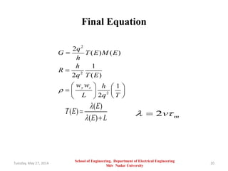
This document summarizes Praveen Dwivedi's M.Tech thesis on modeling silicon nanowire mobility and resistance under the guidance of Dr. Sitangshu Bhattacharya. It introduces nanoelectronics and discusses the physics of nanodevices using the Landauer-Datta model. It also describes modeling silicon nanowire characteristics like electrical resistance and mobility by considering scattering mechanisms like lattice scattering and intervalley scattering. The document outlines Dwivedi's work on developing analytical models to determine the role of first-order intervalley scattering in silicon nanowire electrical resistance.


![Description of Silicon nanowire according to ITRS
[2,3]
Potential Value of Material
Low surface scattering due to one dimensional.
High control of Leakage by Gate.
Key challenges
Nanowires has key challenge to grow in desired location and
desired direction.
Nanowires has challenge of catalyst compatible with CMOS
processing.
Challenge for dope nanowires channel and source/ drain regions.
Challenge to achieve the high, electron and hole mobility on
silicon.
Challenge in pattern surround gate structure .
[Source-ITRS]
Tuesday, May 27, 2014 7
School of Engineering, Department of Electrical Engineering
Shiv Nadar University](https://image.slidesharecdn.com/finalm-140527060054-phpapp01/85/Final-m-tech-ppt_praveen-7-320.jpg)
![Key Factors (advantages) of Silicon Nanowires
Cost -effective bottom-up fabrication
Higher carrier mobility by reduction of scattering due to
crystalline structure.
Smooth surface and ability to produce radial and axial
nanowires heterostructure.
Better scalability resulting from the fact that diameter of
nanowires can be controlled down to below 10nm.
[Refe-3]
Tuesday, May 27, 2014 8
School of Engineering, Department of Electrical Engineering
Shiv Nadar University](https://image.slidesharecdn.com/finalm-140527060054-phpapp01/85/Final-m-tech-ppt_praveen-8-320.jpg)


![References
8. Soshi Sato, “A Study on Electrical Characteristics of Silicon Nanowire Field Effect Transistors” Ph.D.
dissertation Tokyo institute of technology, 2008.
9. Allon I. Hochbaum, Renkun Chen, Raul Diaz Delgado, Wenjie Liang, Erik C. Garnett, Mark Najarian3,Arun
Majumdar&Peidong Yang “Enhanced thermoelectric performance of rough silicon nanowires”Vol 451| 10
January 2008|,pp.163-167, doi:10.1038/nature06381.
10. Yonatan Calahorra, “Electrical and Mechanical Propertiesof Silicon Nanowires”, Master of Science
dissertation, Israel Institute of Technology February 2010 pp. 5-30.
11. “Intel reinvents transistors using new 3-D structure” , Available online.
12. Y. Li, K. Buddharaju, B. C. Tinh, N. Singh, and S. J. Lee, “Improvedvertical silicon nanowire based
thermoelectric power generator with polyimide filling”, IEEE Electron Dev. Lett., vol.33, pp. 715-717,
(2012).
13. A. K. Buin, A. Verma, A. Svizhenko and M. P. Anantram, “Significant Enhancement of Hole Mobility in
[110] Silicon Nanowires, Compared to Electrons and Bulk Silicon”, Nano Lett., vol. 8, pp. 760-765, (2008).
14. E. B. Ramayya, D. Vasileska, S. M. Goodnick and I. Knezevic, “Electron transport in silicon nanowires:
The role of acoustic phonon confinement and surface roughness scattering”, J. Appl. Phys., vol. 104, pp.
063711 (1)-(12), (2008).
Tuesday, May 27, 2014 44
School of Engineering, Department of Electrical Engineering
Shiv Nadar University](https://image.slidesharecdn.com/finalm-140527060054-phpapp01/85/Final-m-tech-ppt_praveen-44-320.jpg)


![My Work for 4th Semester
• In Part 1 We Calculated the mobility of silicon nanowires under the
influence of intra & intervalley scattering has been presented.
• In part 2 we Calculated the current for [100] Oriented silicon Nanowire by
Non equilibrium Green’s Function (NEGF) and Atomistix ToolKit (ATK).
Tuesday, May 27, 2014 55
NanoScale Electro thermal Laboratory Department of Electrical Engineering
Shiv Nadar University](https://image.slidesharecdn.com/finalm-140527060054-phpapp01/85/Final-m-tech-ppt_praveen-55-320.jpg)


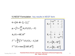
![Part II
• Under this work we calculated the Electrical current [100]
Oriented Silicon Nanowire by the Non-equilibrium Green’s
Function Method (NEGF) and Atomistix Tool Kit(ATK).
Tuesday, May 27, 2014 60
NanoScale Electro thermal Laboratory Department of Electrical Engineering
Shiv Nadar University](https://image.slidesharecdn.com/finalm-140527060054-phpapp01/85/Final-m-tech-ppt_praveen-60-320.jpg)


![VTU Internship Report.[Peekay Steel Castings]](https://cdn.slidesharecdn.com/ss_thumbnails/internshipreport-1hk15me076-200402094020-thumbnail.jpg?width=640&height=640&fit=bounds)


![MTech Seminar Presentation [IIT-Bombay]](https://cdn.slidesharecdn.com/ss_thumbnails/seminar-presentation-final-140502111554-phpapp02-thumbnail.jpg?width=640&height=640&fit=bounds)


![Behaviour of frp confined normal and high strength concrete [autosaved]](https://cdn.slidesharecdn.com/ss_thumbnails/behaviouroffrp-confinednormalandhighstrengthconcreteautosaved-140303104936-phpapp01-thumbnail.jpg?width=640&height=640&fit=bounds)


