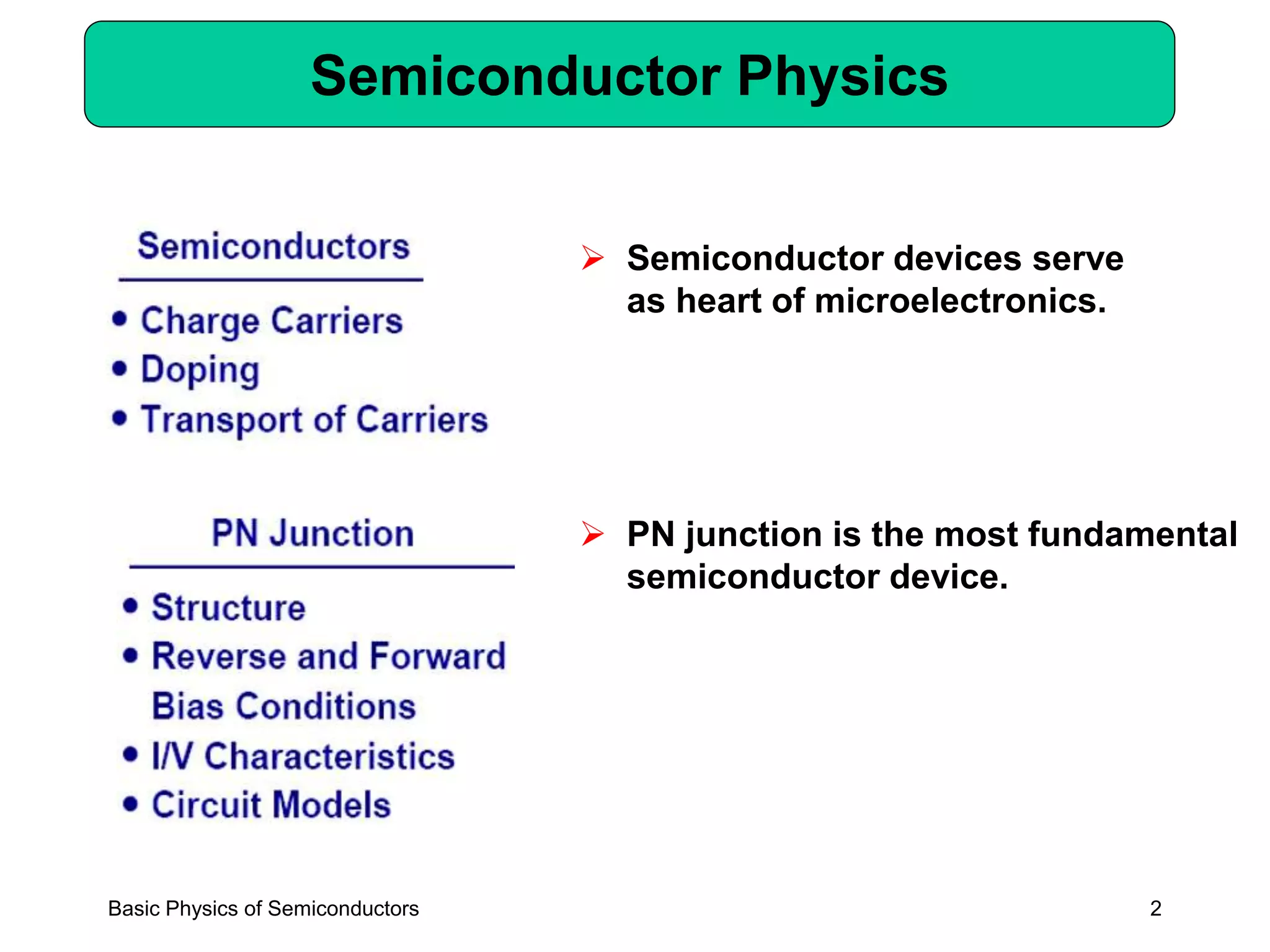
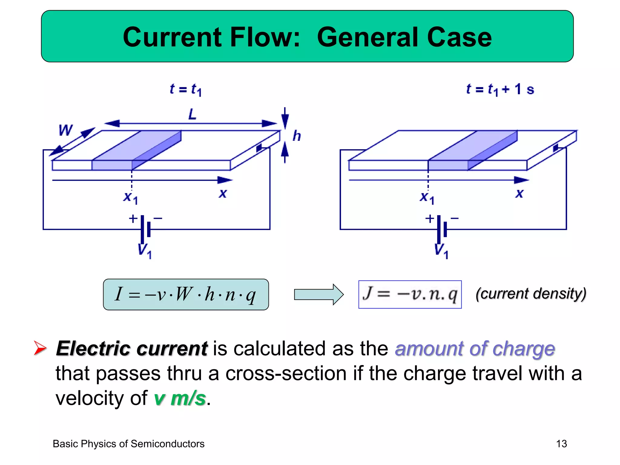
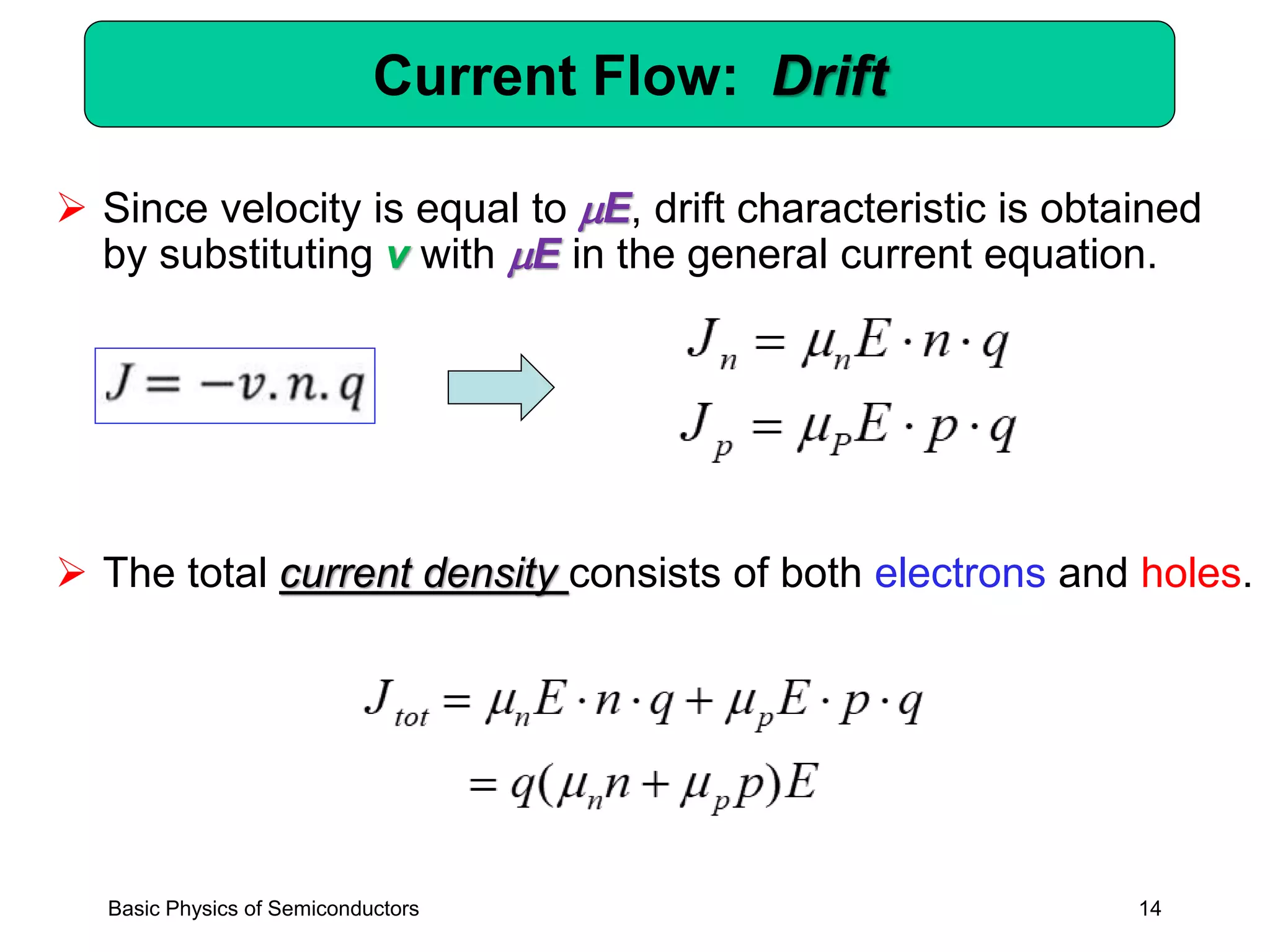
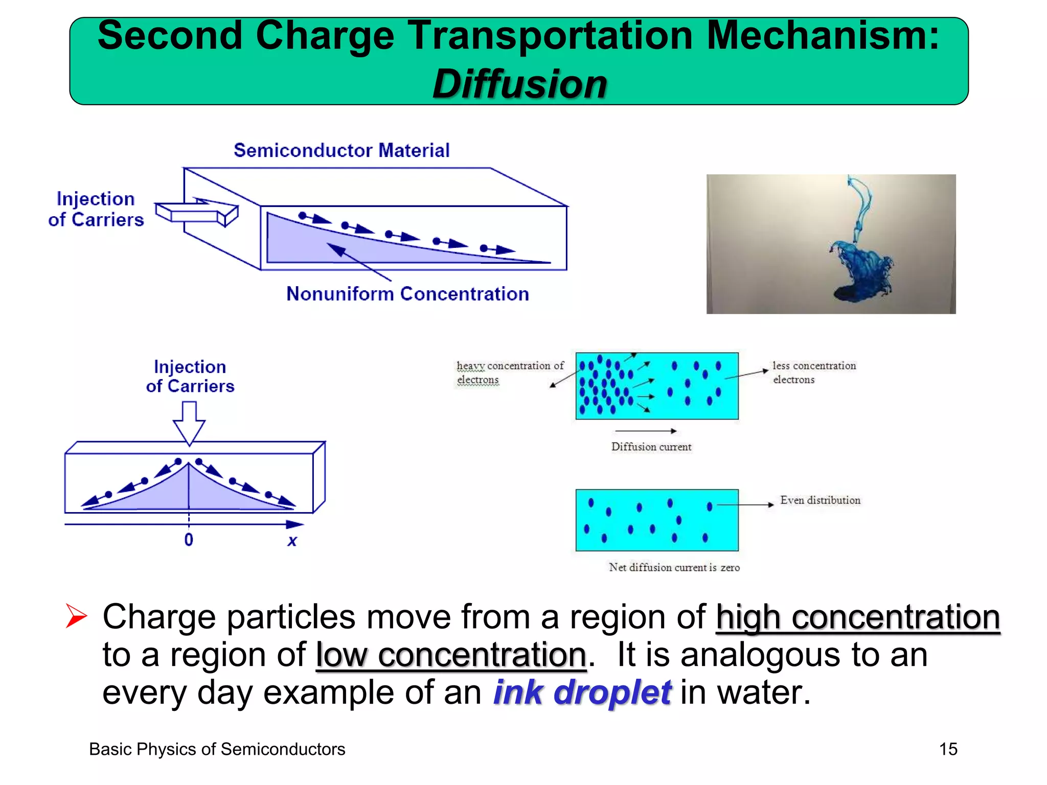
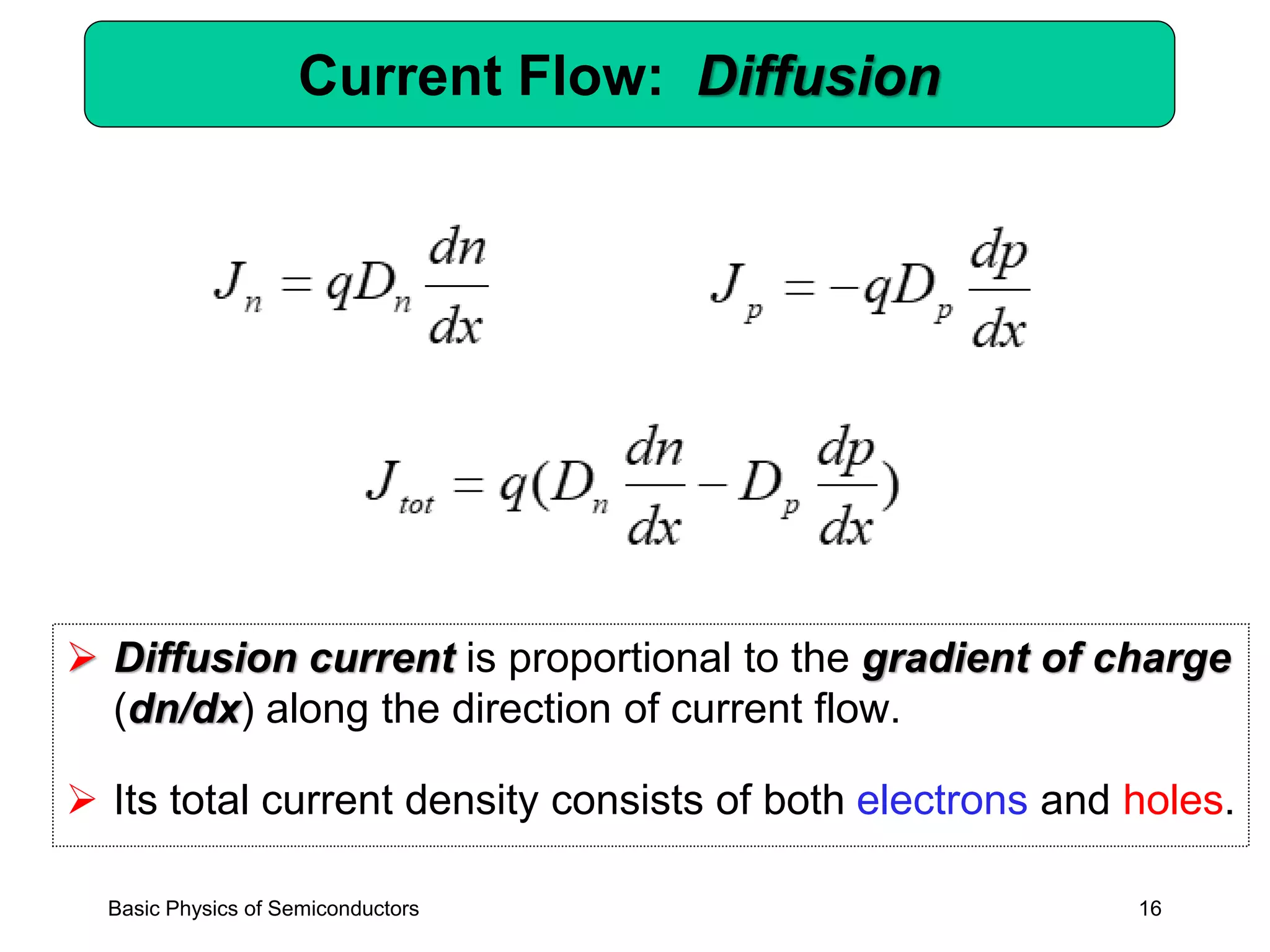
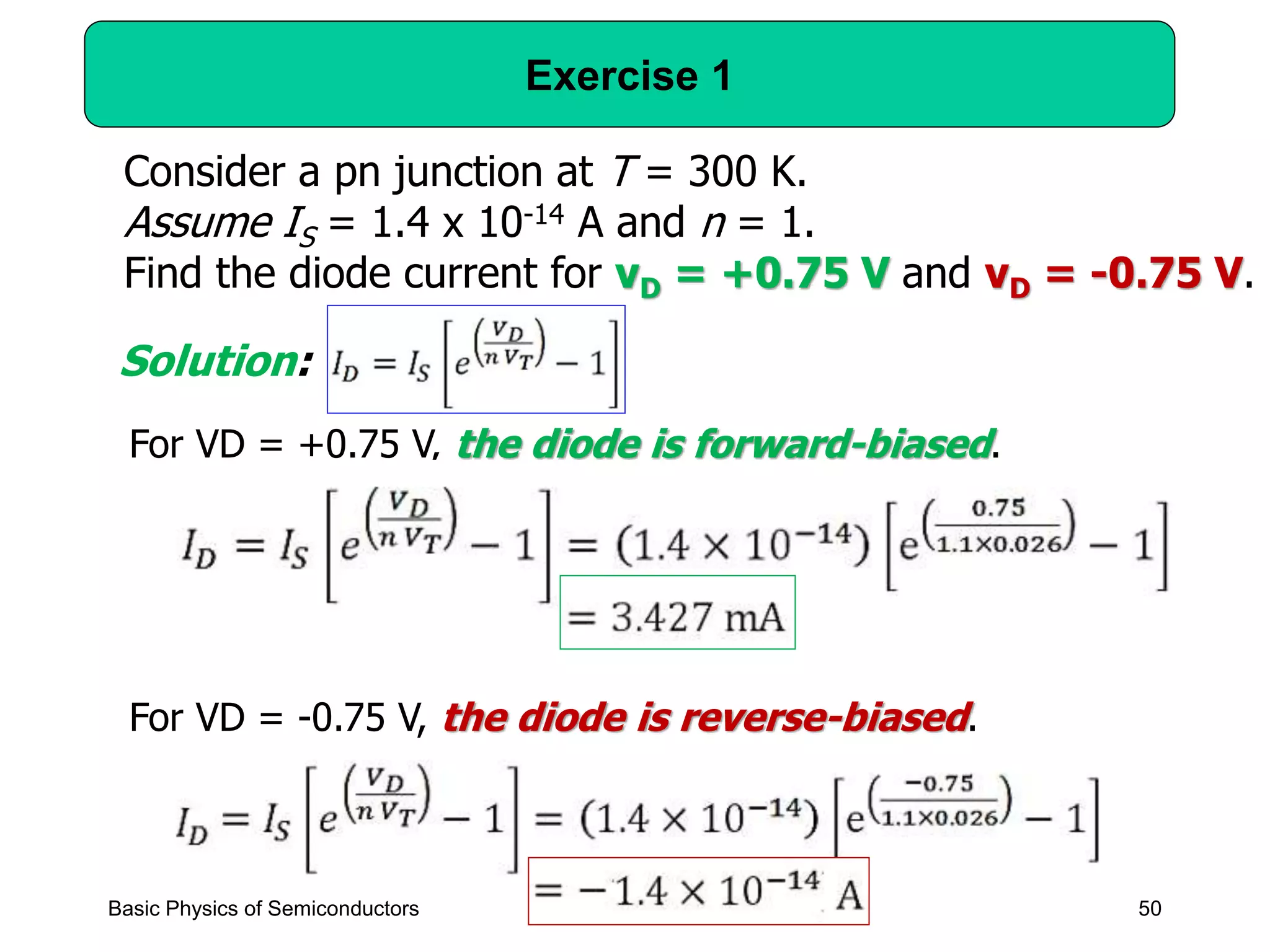
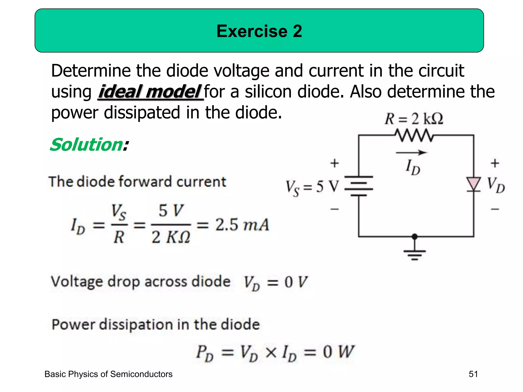
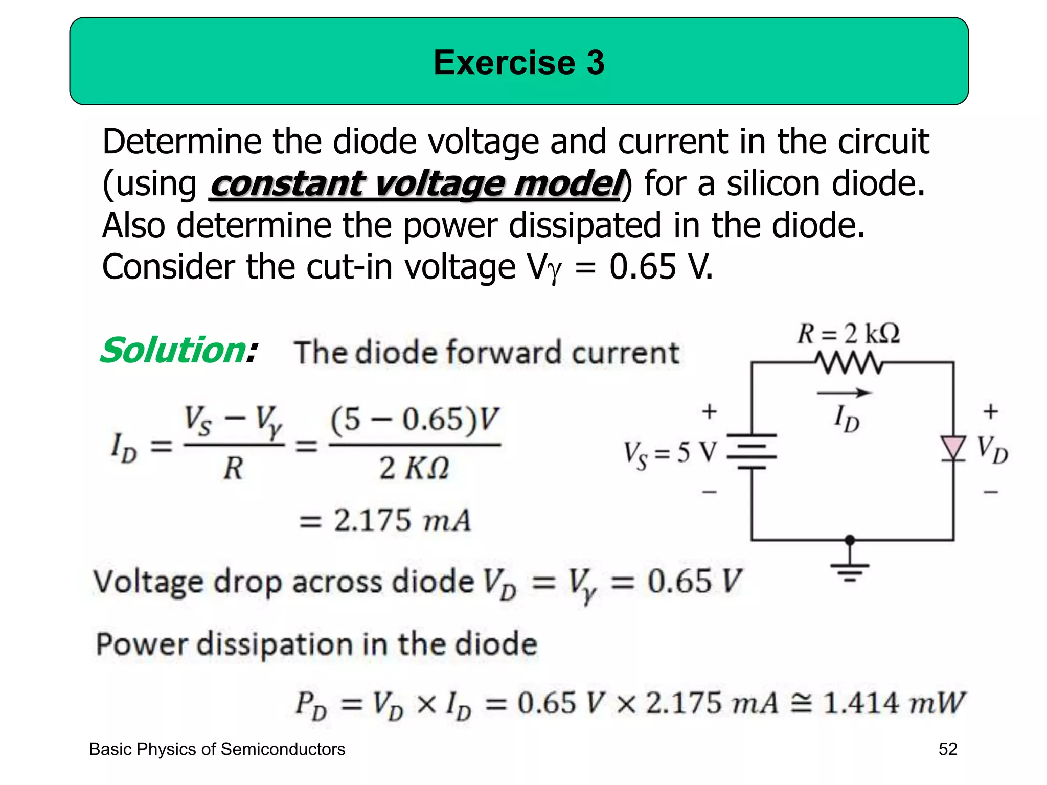
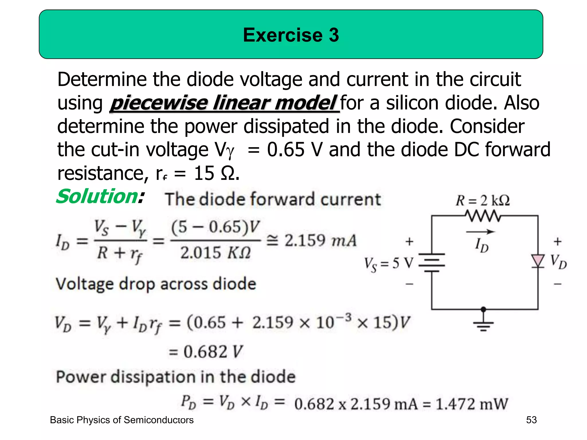
This document provides an overview of basic semiconductor physics concepts including charge carriers in semiconductors, doping, electron-hole pair generation, free electron density, PN junctions, and diode characteristics. Key points covered include:
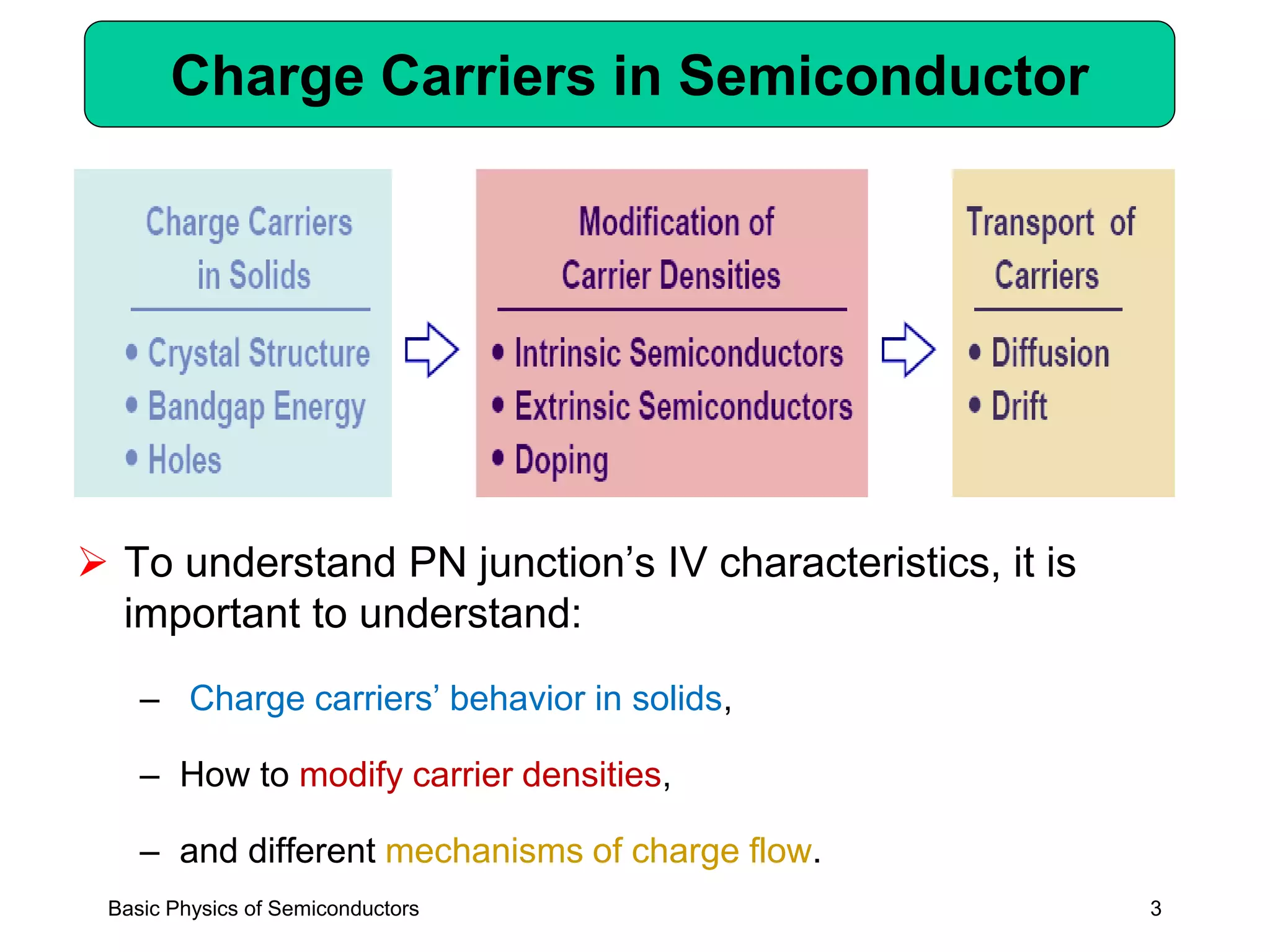
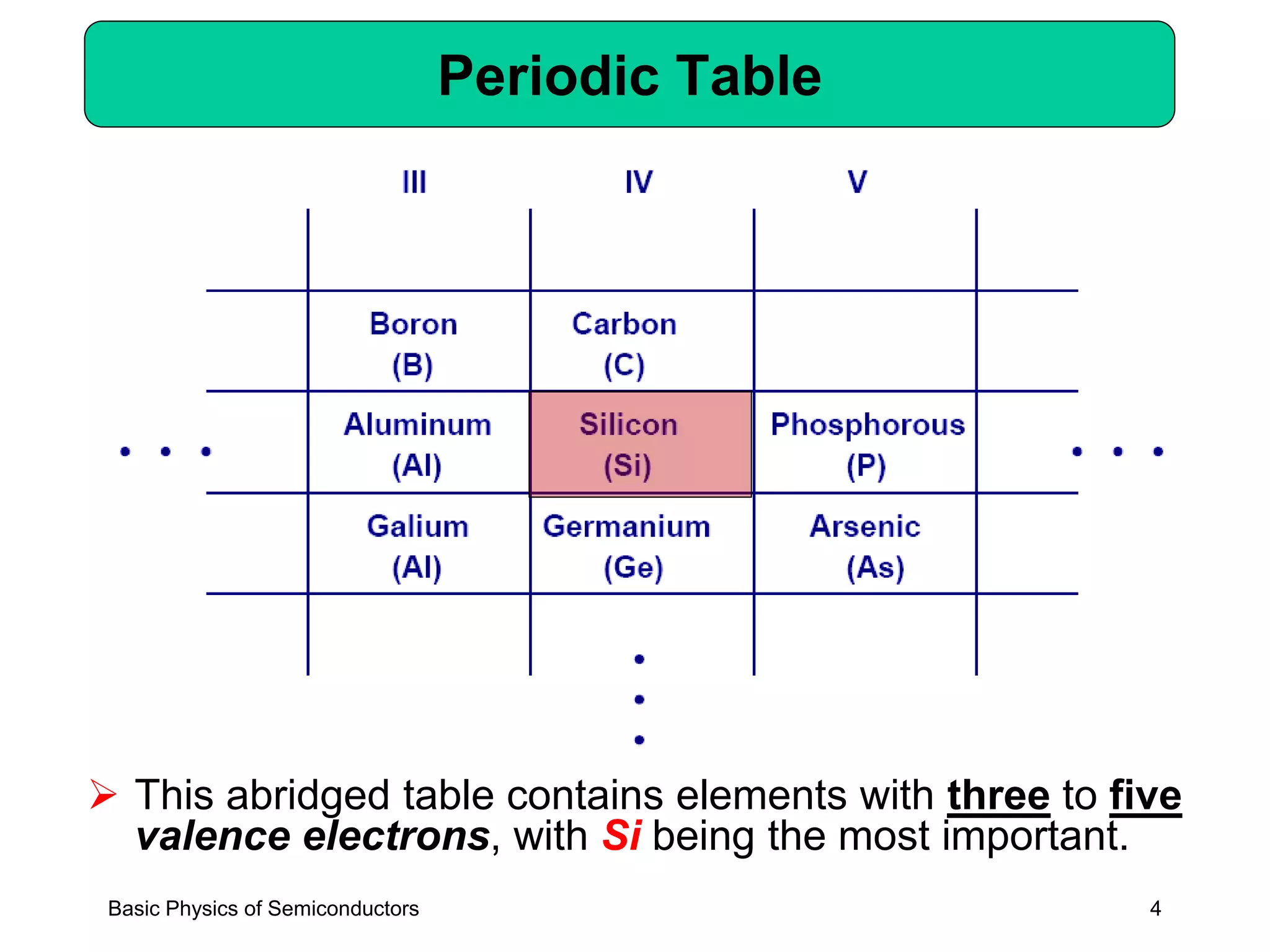
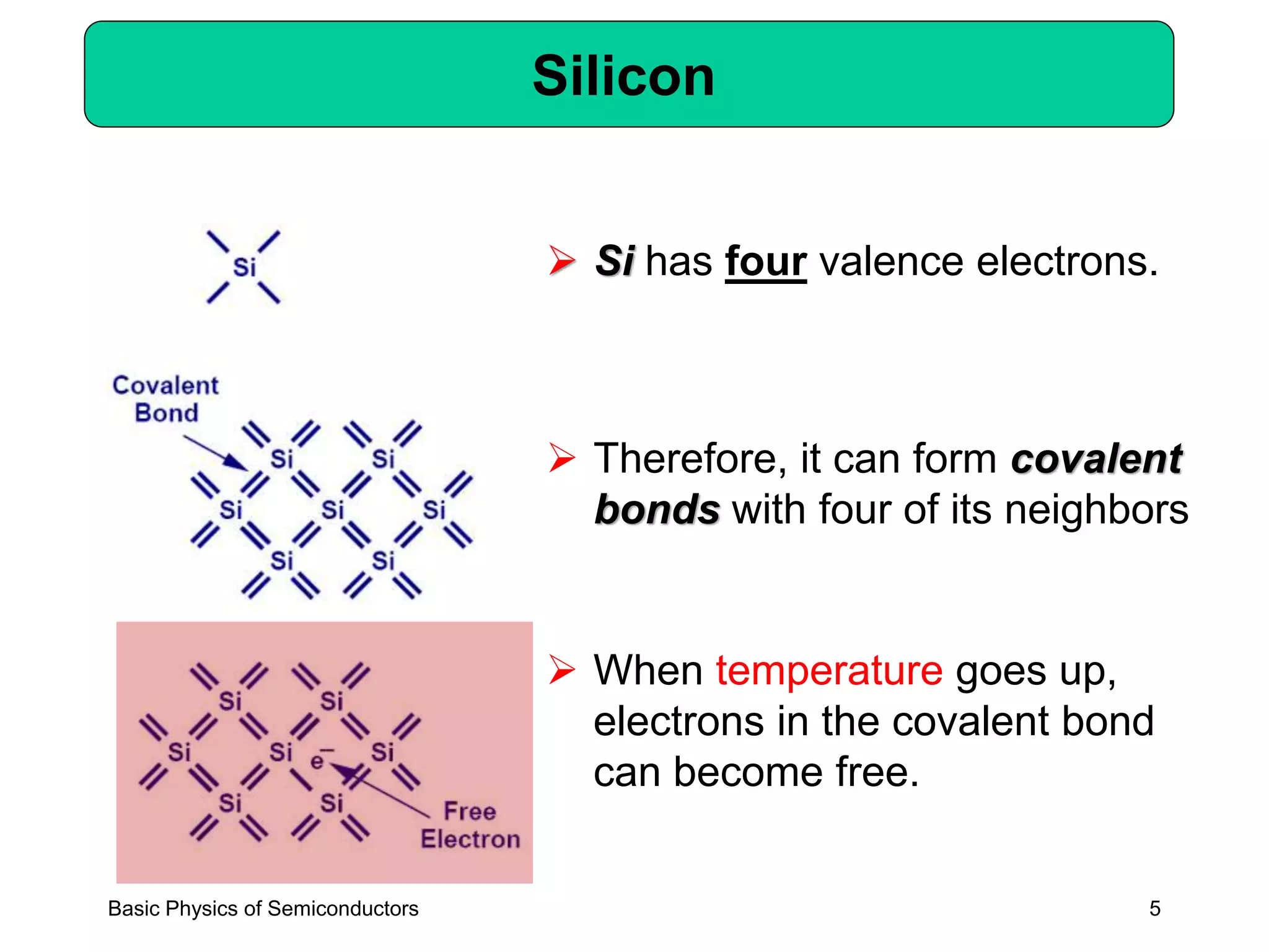
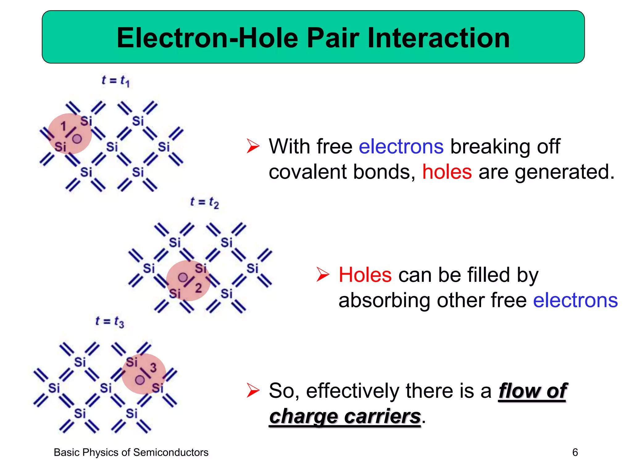
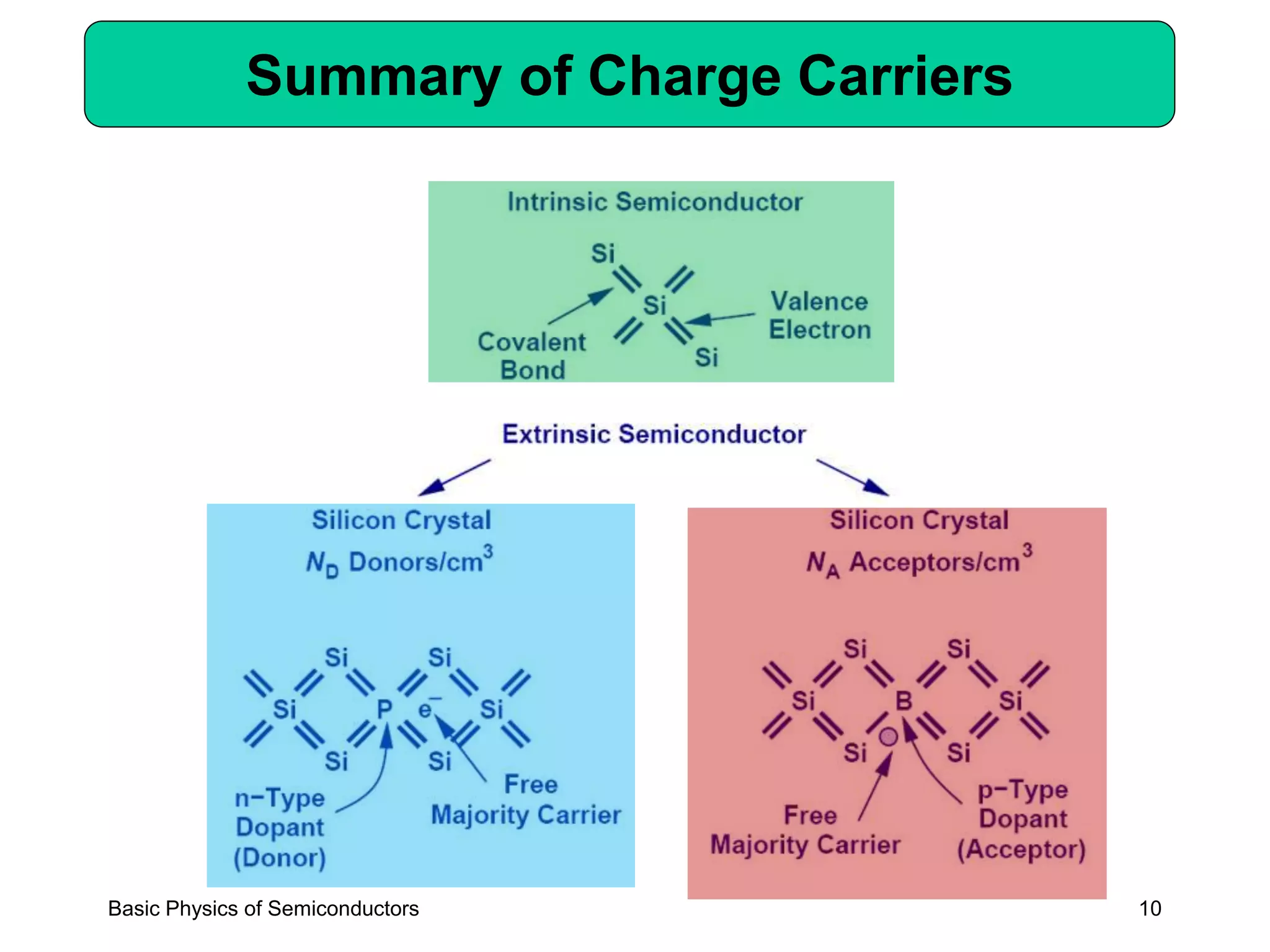
- Semiconductors have movable charge carriers that allow control of conductivity through doping. Silicon is the most important semiconductor and forms covalent bonds with four neighbors.
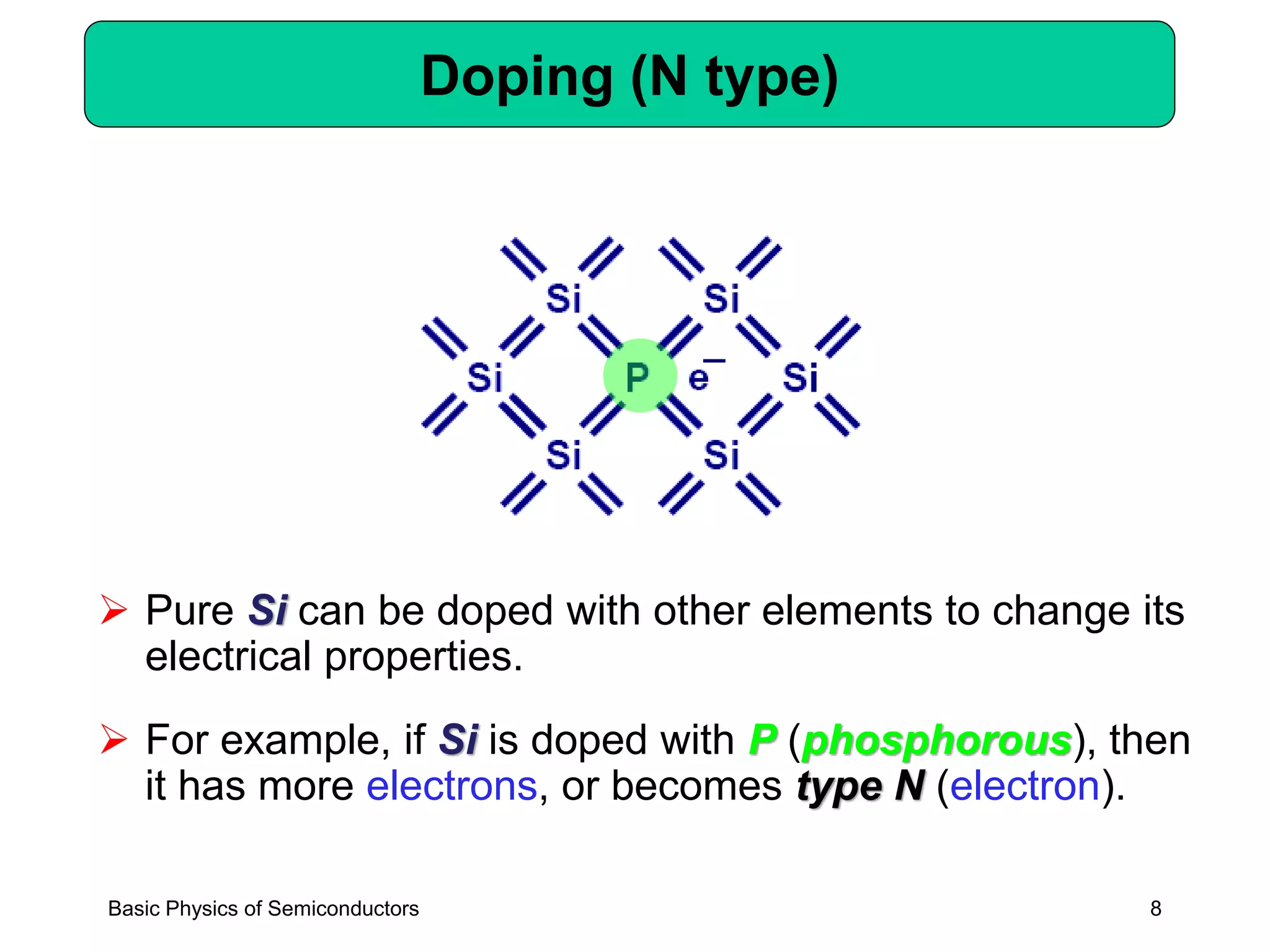
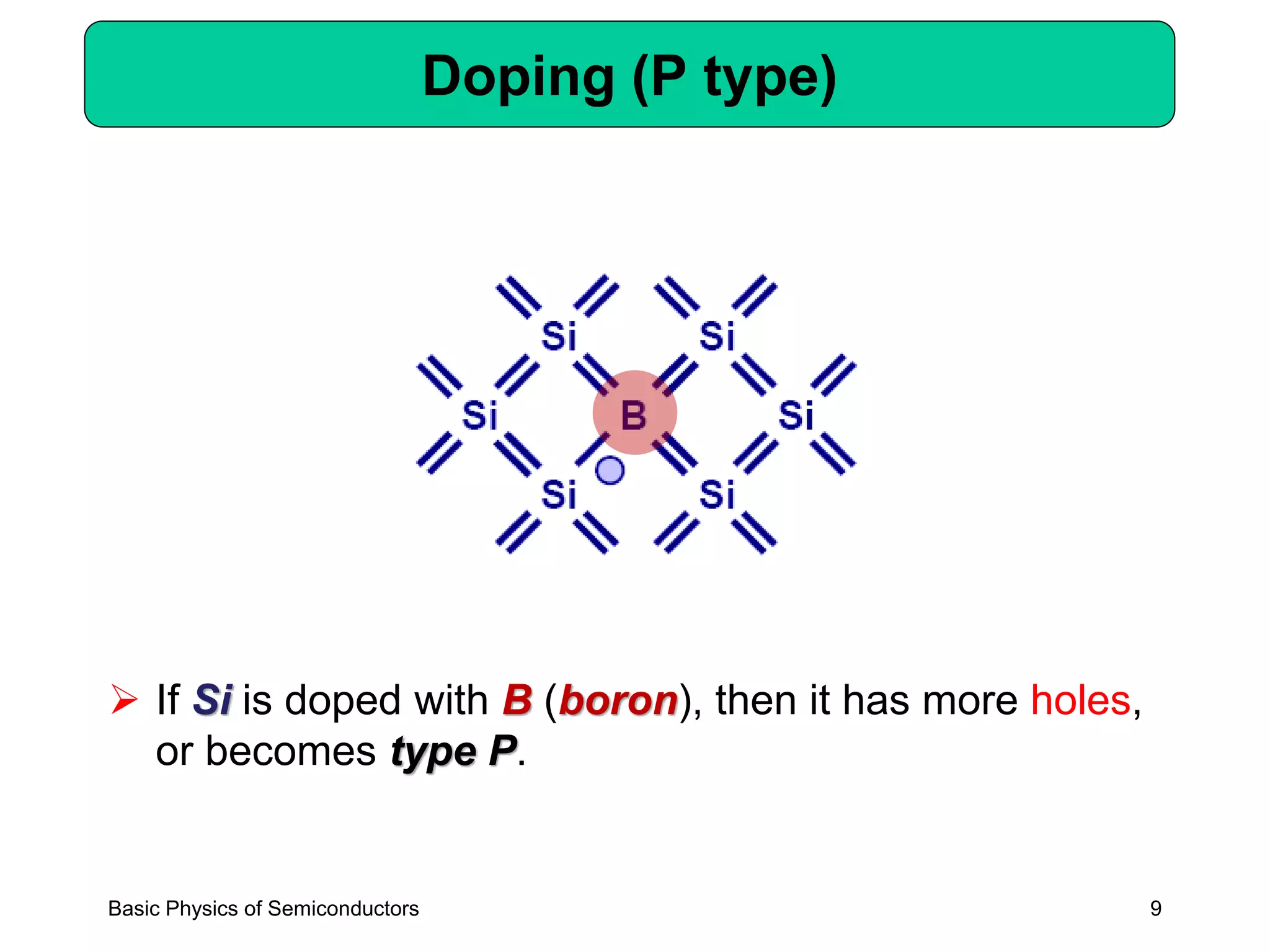
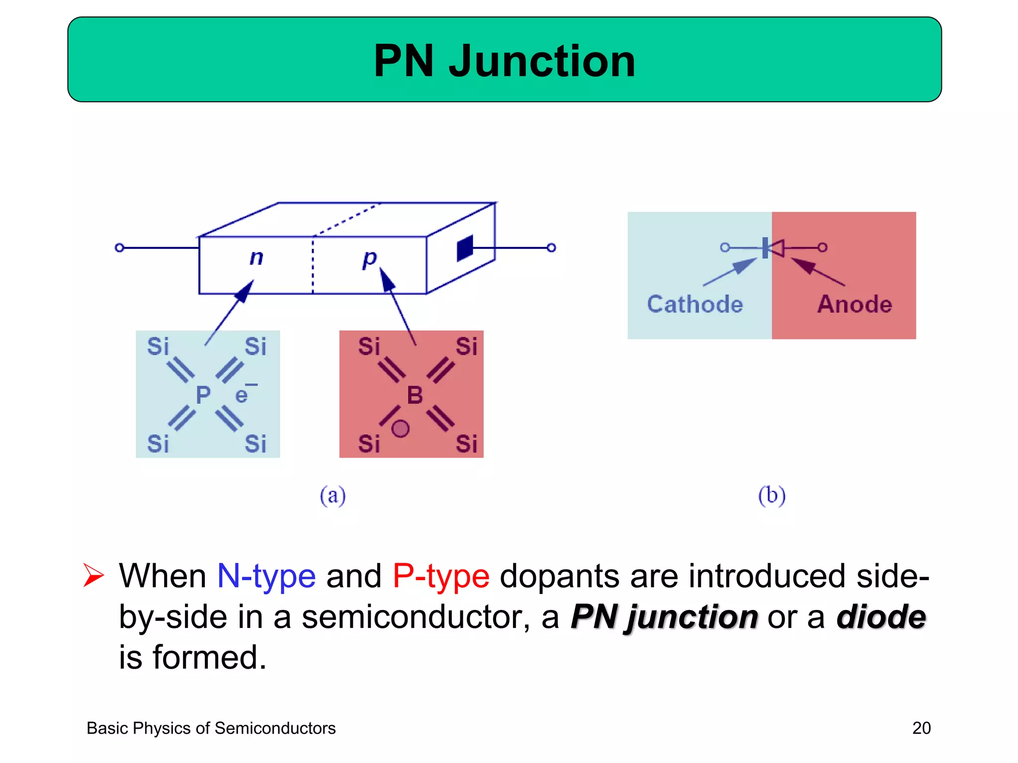
- Doping silicon with elements like phosphorus (N-type) or boron (P-type) introduces free electrons or holes that determine whether it acts as an N-type or P-type semiconductor.
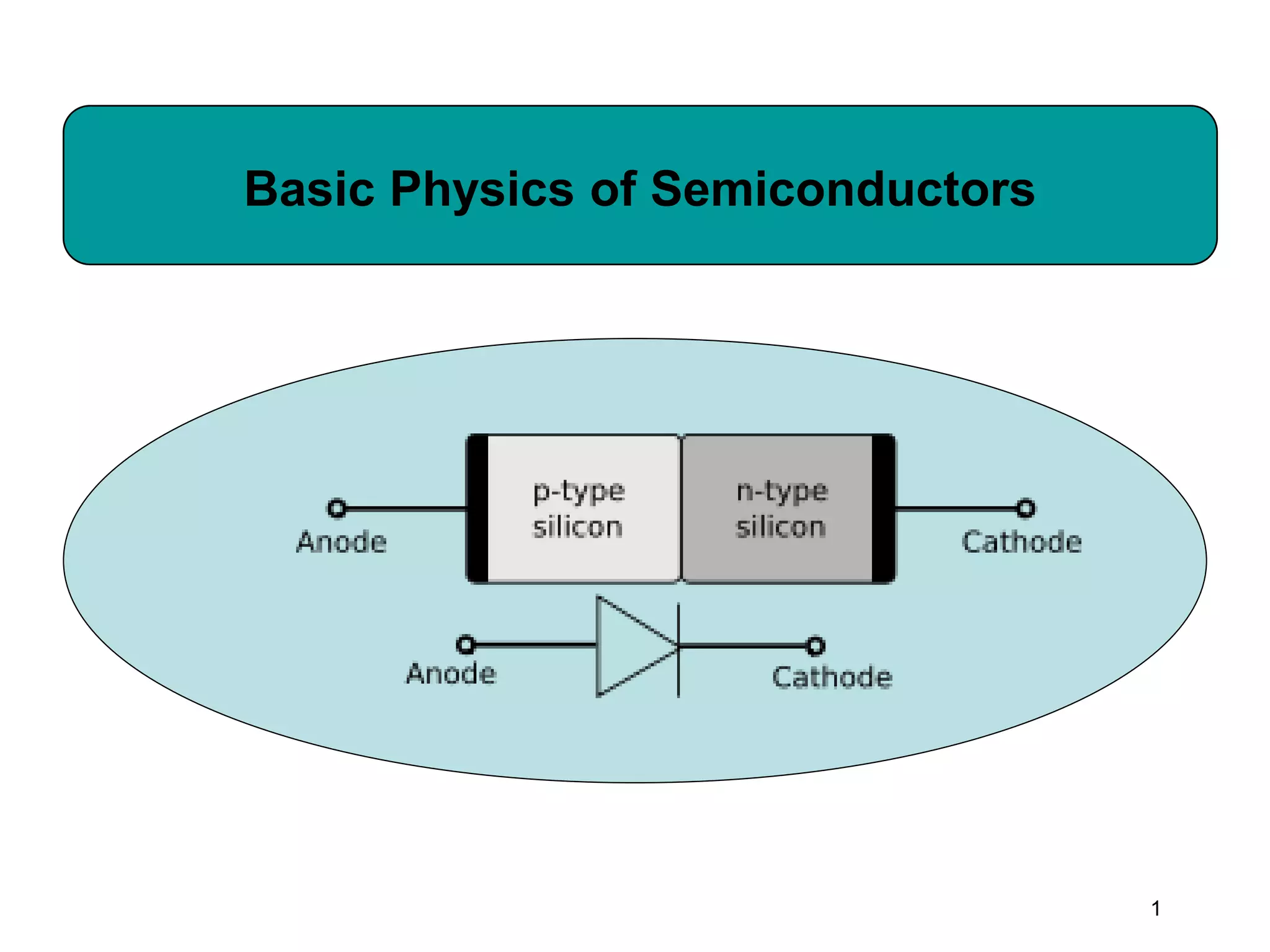
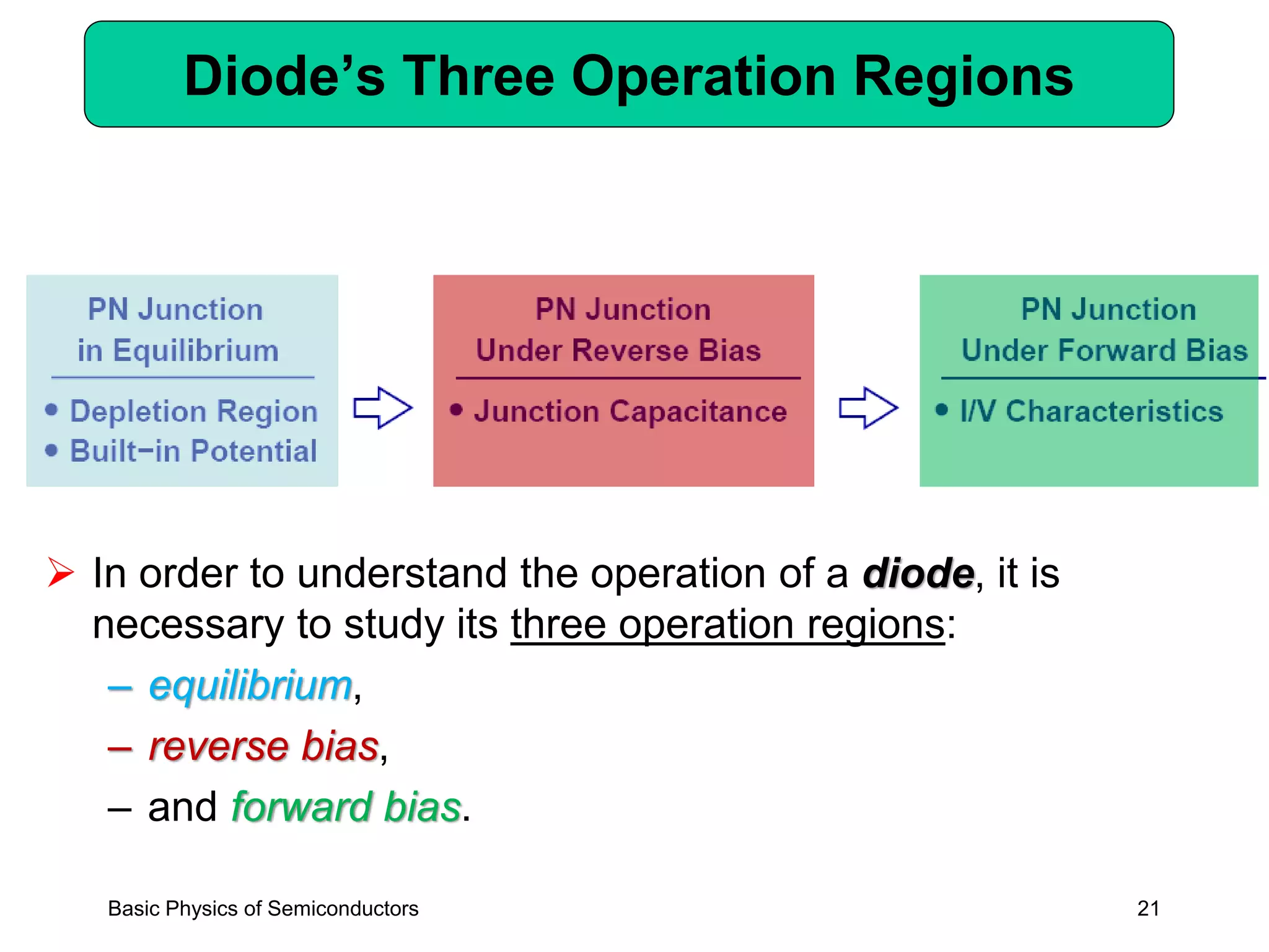
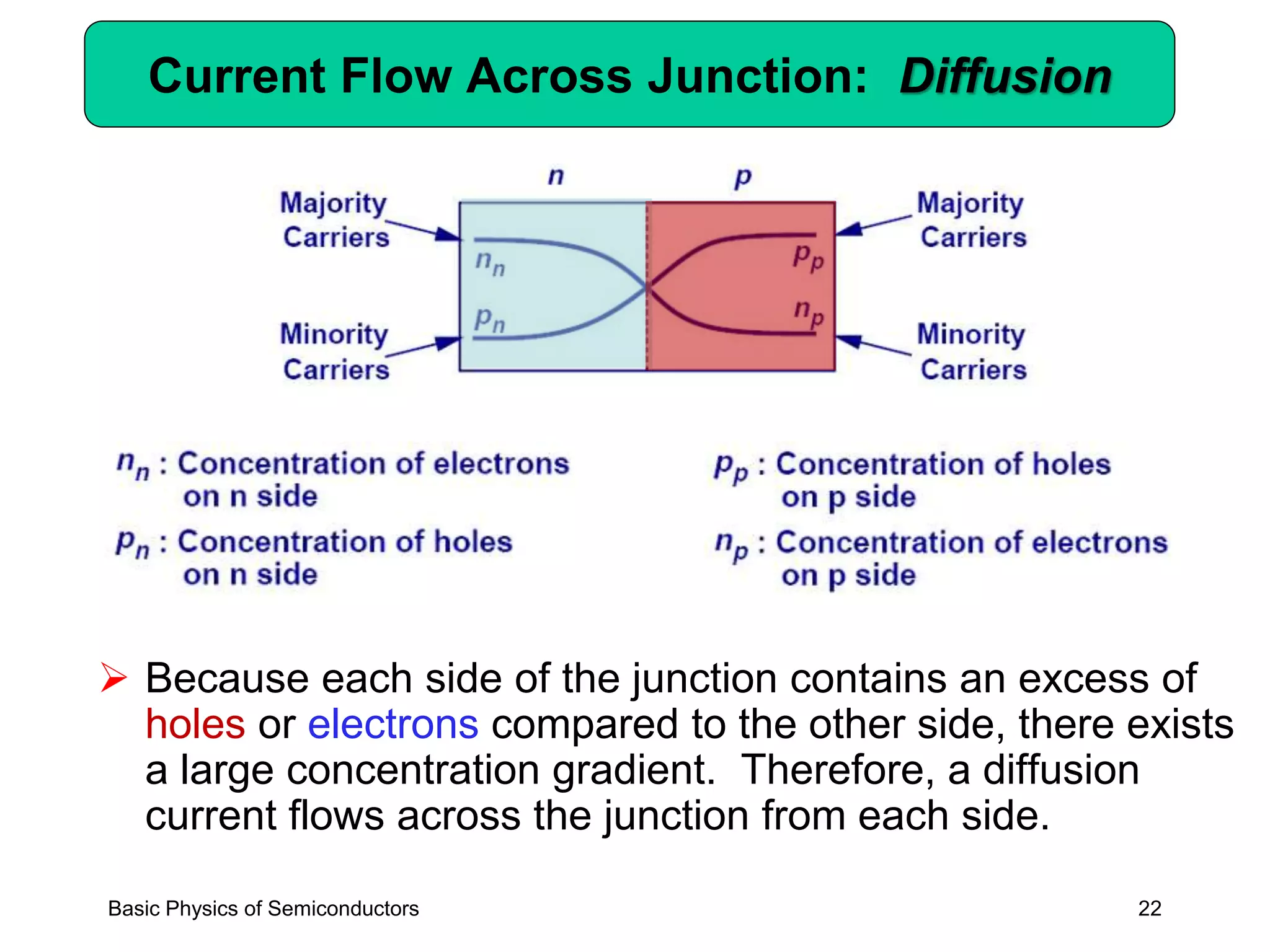
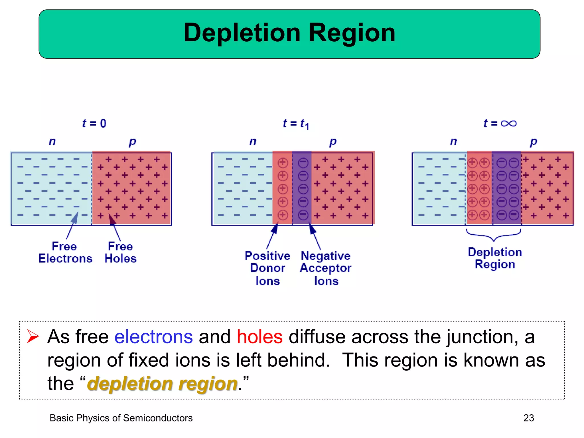
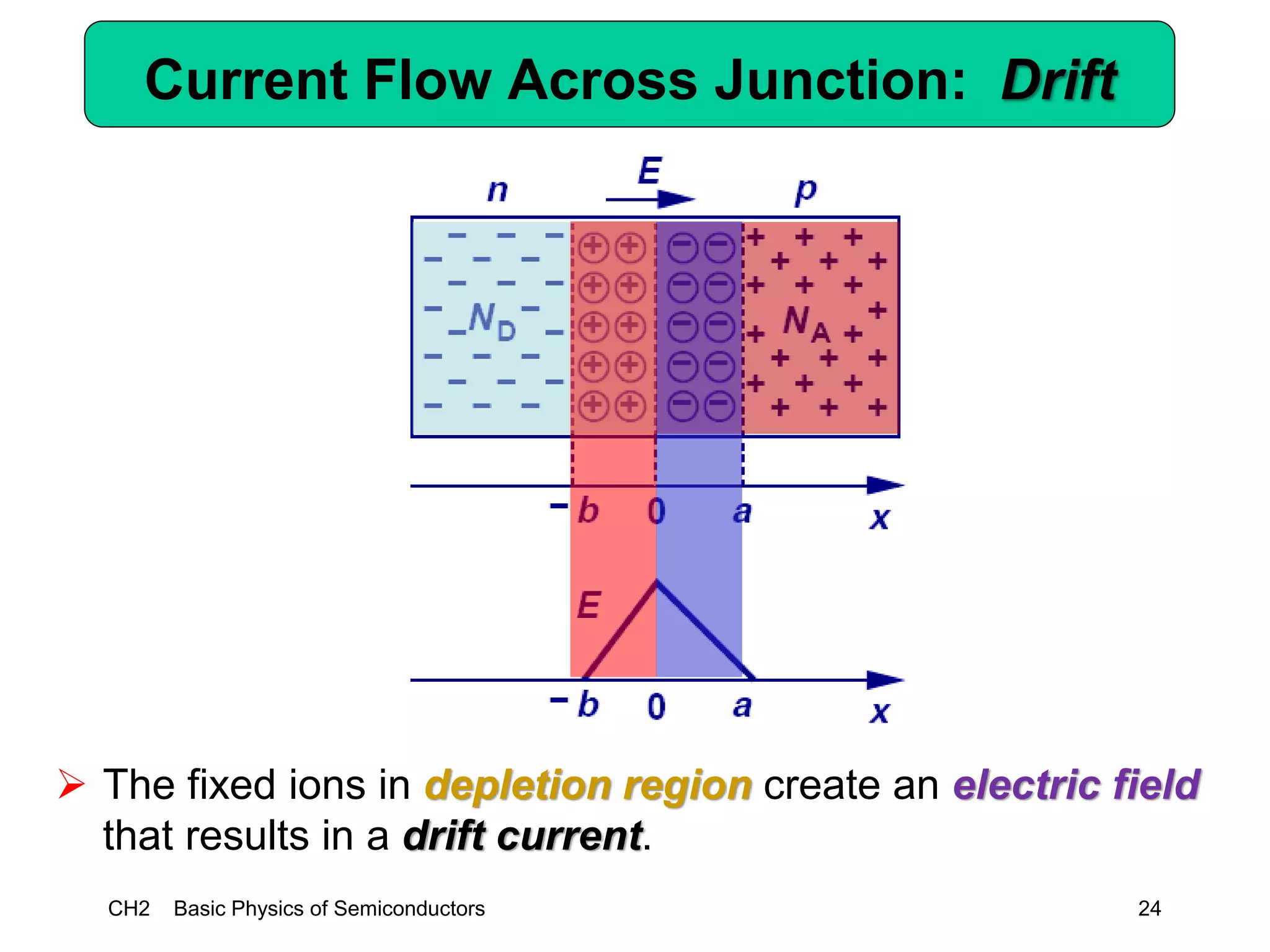
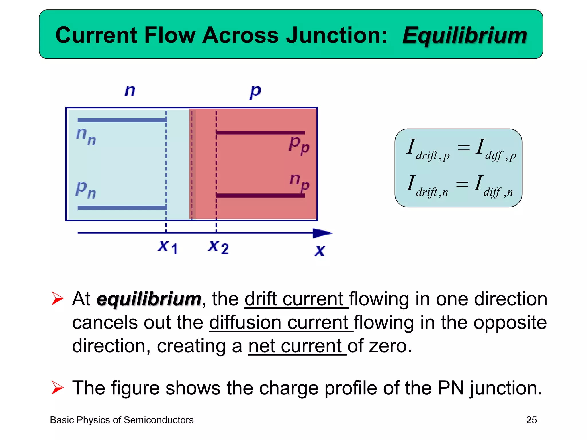
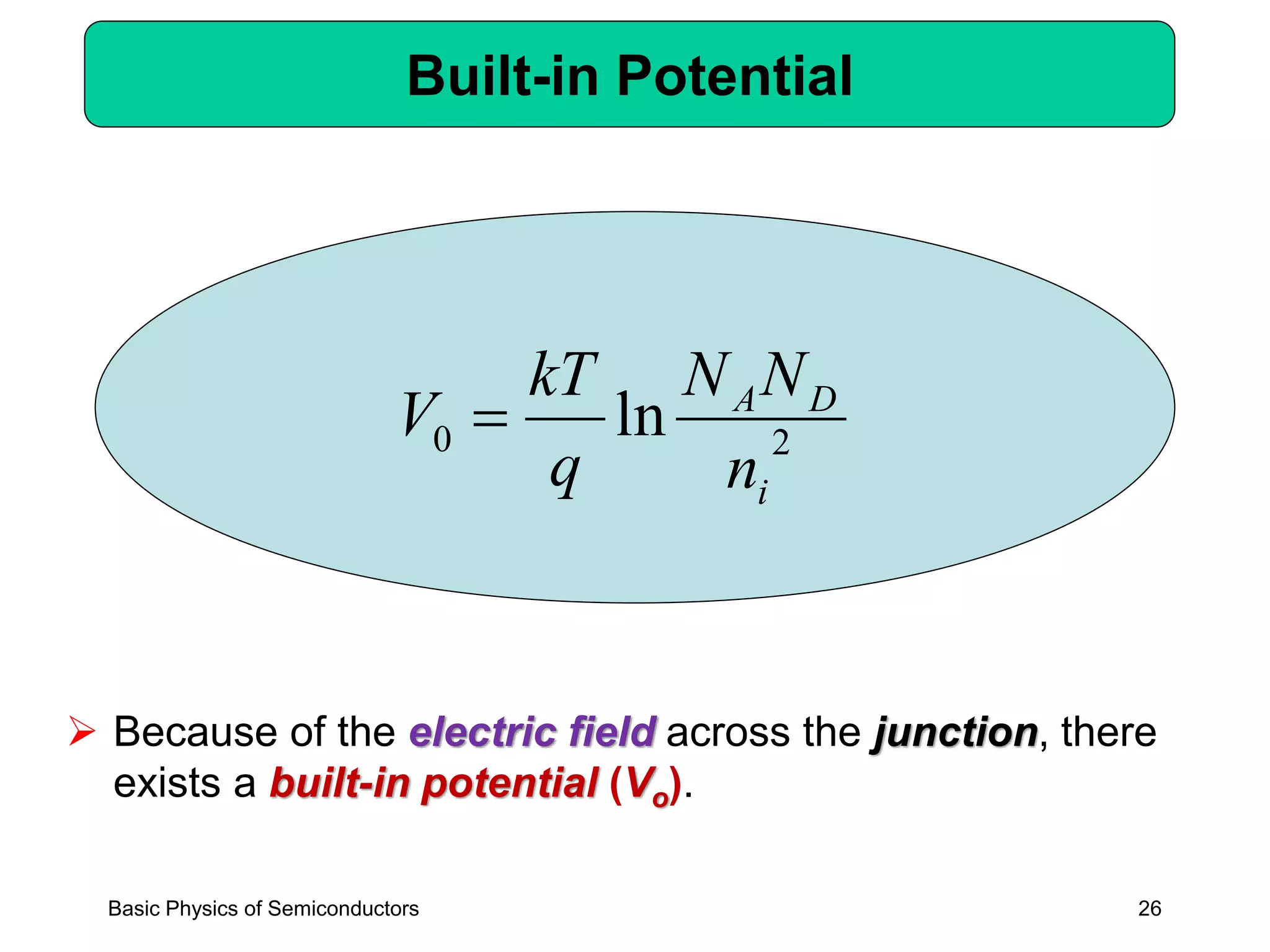
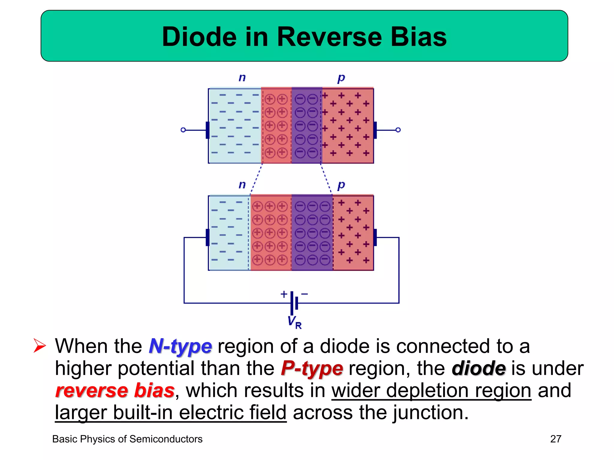
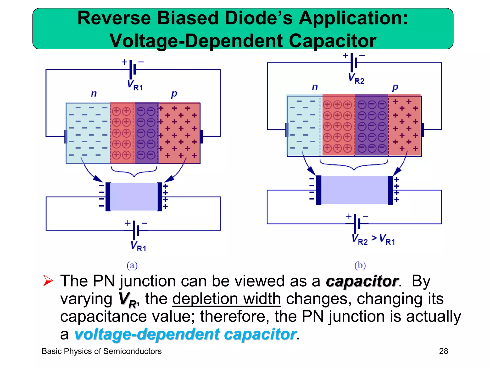
- A PN junction forms at the interface between P-type and N-type materials