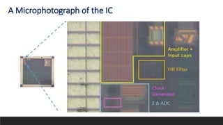
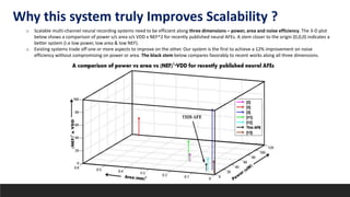
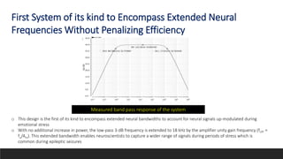
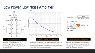
This document summarizes a research paper on developing an efficient multi-channel neural recording system. The system aims to integrate neural recording devices, rapid data analysis to detect seizure onsets, and signal injection to mitigate seizures into an implantable system. Key challenges addressed include scalability, safety standards, power limitations, and noise. The proposed system uses a low-power, low-noise amplifier and second-order delta-sigma ADC per channel, along with a digital FIR filter. Testing showed the system achieves 12% better noise efficiency than prior work, addressing scalability challenges across power, area, and noise.


![Comparison: Electrode area vs. Size of Skull
Power Breakup of each module in a multi-
channel neural signal acquisition system
Source: Wattanapatich, Fee & Sarpeshkar,
[Massachusetts Institute of Technology]
Source: Chandler, Farshchi & Judy,
[University of California, Los Angeles]
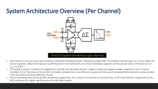
Constraints of Building a Neural System](https://image.slidesharecdn.com/efficientsignalacquisitioninmulti-channelneuralsystems-200819023527/85/Efficient-signal-acquisition-in-multi-channel-neural-systems-4-320.jpg)
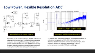
![Low Power, Flexible Resolution ADC
Circuit implementation of the ΣΔ ADC
Self-biased differential
inverters with auxiliary CMFB
Source: Wang and Theogarajan,
[University of California, Santa Barbara]
The ∆∑ ADC is implemented with the Boser Wooley Architecture
with 1-bit comparator. The integrators in the ADC (shown in red)
are implemented using self biased super inverters which
alleviates the need for bias circuits and being robust across
process corners.
The superinverter as is has weak
common mode feedback. For an ADC
clocked at a few MHz, the common
mode settling of the superinverter is not
fast enough. To alleviate this, a auxillary
switched capacitor CMFB is introduced
to the superinverters. This produced a
fast CMFB settling ensuring that
common mode is stable.](https://image.slidesharecdn.com/efficientsignalacquisitioninmulti-channelneuralsystems-200819023527/85/Efficient-signal-acquisition-in-multi-channel-neural-systems-9-320.jpg)