The document describes an electronics course covering various electronic devices. It discusses the objectives of acquainting students with the construction, theory and operation of basic devices like PN junction diodes, bipolar junction transistors, field effect transistors, and other optoelectronic devices. The document outlines 5 units that will be covered: semiconductor diodes, bipolar junction transistors, field effect transistors, special semiconductor devices, and power devices and displays. It lists recommended textbooks and references.
PN junction diode –structure, operation and V-I characteristics, diffusion and transient capacitance - Rectifiers – Half Wave and Full Wave Rectifier,– Display devices- LED, Laser diodes- Zener diodecharacteristics-Zener Reverse characteristics – Zener as regulator,TRANSISTORS, BJT, JFET, MOSFET- structure, operation, characteristics and Biasing UJT, Thyristor and IGBT Structure and characteristics,BJT small signal model – Analysis of CE, CB, CC amplifiers- Gain and frequency response –
MOSFET small signal model– Analysis of CS and Source follower – Gain and frequency response- High frequency analysis,BIMOS cascade amplifier, Differential amplifier – Common mode and Difference mode analysis – FET input stages – Single tuned amplifiers – Gain and frequency response – Neutralization methods, power amplifiers –Types (Qualitative analysis),Advantages of negative feedback – voltage / current, series , Shunt feedback –positive feedback – Condition for oscillations, phase shift – Wien bridge, Hartley, Colpitts and Crystal oscillators.
The Performance of an Integrated Transformer in a DC/DC ConverterTELKOMNIKA JOURNAL
The separation between the low-voltage part and high-voltage part of the converter is formed by a
transformer that transfers power while jamming the DC ring. The resonant mode power oscillator is utilized
to allow elevated competence power transfer. The on-chip transformer is probable to have elevated value
inductance, elevated quality factors and elevated coupling coefficient to decrease the loss in the
oscillation. The performance of a transformer is extremely dependent on the structure, topology and other
essential structures that create it compatible with the integrated circuits IC process such as patterned
ground shield (PGS). Different types of transformers are modeled and simulated in MATLAB; the
performances are compared to select the optimum design. The on-chip transformer model is simulated
and the Results of MATLAB simulation are exposed, showing an excellent agreement in radio frequency
RF.
100 watt inverter using IC CD4047 and MOSFET IRF540
CD 4047 is a low power CMOS astable/monostable multivibrator IC. Here it is wired as an astable multivibrator producing two pulse trains of 0.01s which are 180 degrees out of phase at the pins 10 and 11 of the IC. Pin 10 is connected to the gate of Q1 and pin 11 is connected to the gate of Q2. Resistors R3 and R4 prevents the loading of the IC by the respective MOSFETs. When pin 10 is high Q1 conducts and current flows through the upper half of the transformer primary which accounts for the positive half of the output AC voltage. When pin 11 is high Q2 conducts and current flows through the lower half of the transformer primary in opposite direction and it accounts for the negative half of the output AC voltage.
DESIGN OF DIFFERENT DIGITAL CIRCUITS USING SINGLE ELECTRON DEVICESmsejjournal
Single Electron transistor (SET) is foreseen as an excellently growing technology. The aim of this paper is
to present in short the fundamentals of SET as well as to realize its application in the design of single
electron device based novel digital logic circuits with the help of a Monte Carlo based simulator. A Single
Electron Transistors (SET) is characterized by two most substantial determinants. One is very low power
dissipation while the other is its small stature that makes it a favorable suitor for the future generation of
very high level integration. With the utilization of SET, technology is moving past CMOS age resulting in
power efficient, high integrity, handy and high speed devices. Conducting a check on the transport of single
electrons is one of the most stirring aspects of SET technologies. Apparently, Monte Carlo technique is in
vogue in terms of simulating SED based circuits. Hence, a MC based tool called SIMON 2.0 is exercised
upon for the design and simulation of these digital logic circuits. Further, an efficient functioning of the
logic circuits such as multiplexers, decoders, adders and converters are illustrated and established by
means of circuit simulation using SIMON 2.0 simulator.
Unit 8 - Information and Communication Technology (Paper I).pdfThiyagu K
This slides describes the basic concepts of ICT, basics of Email, Emerging Technology and Digital Initiatives in Education. This presentations aligns with the UGC Paper I syllabus.
How to Split Bills in the Odoo 17 POS ModuleCeline George
Bills have a main role in point of sale procedure. It will help to track sales, handling payments and giving receipts to customers. Bill splitting also has an important role in POS. For example, If some friends come together for dinner and if they want to divide the bill then it is possible by POS bill splitting. This slide will show how to split bills in odoo 17 POS.
2024.06.01 Introducing a competency framework for languag learning materials ...Sandy Millin
http://sandymillin.wordpress.com/iateflwebinar2024
Published classroom materials form the basis of syllabuses, drive teacher professional development, and have a potentially huge influence on learners, teachers and education systems. All teachers also create their own materials, whether a few sentences on a blackboard, a highly-structured fully-realised online course, or anything in between. Despite this, the knowledge and skills needed to create effective language learning materials are rarely part of teacher training, and are mostly learnt by trial and error.
Knowledge and skills frameworks, generally called competency frameworks, for ELT teachers, trainers and managers have existed for a few years now. However, until I created one for my MA dissertation, there wasn’t one drawing together what we need to know and do to be able to effectively produce language learning materials.
This webinar will introduce you to my framework, highlighting the key competencies I identified from my research. It will also show how anybody involved in language teaching (any language, not just English!), teacher training, managing schools or developing language learning materials can benefit from using the framework.
Instructions for Submissions thorugh G- Classroom.pptxJheel Barad
This presentation provides a briefing on how to upload submissions and documents in Google Classroom. It was prepared as part of an orientation for new Sainik School in-service teacher trainees. As a training officer, my goal is to ensure that you are comfortable and proficient with this essential tool for managing assignments and fostering student engagement.
Ethnobotany and Ethnopharmacology:
Ethnobotany in herbal drug evaluation,
Impact of Ethnobotany in traditional medicine,
New development in herbals,
Bio-prospecting tools for drug discovery,
Role of Ethnopharmacology in drug evaluation,
Reverse Pharmacology.
Operation “Blue Star” is the only event in the history of Independent India where the state went into war with its own people. Even after about 40 years it is not clear if it was culmination of states anger over people of the region, a political game of power or start of dictatorial chapter in the democratic setup.
The people of Punjab felt alienated from main stream due to denial of their just demands during a long democratic struggle since independence. As it happen all over the word, it led to militant struggle with great loss of lives of military, police and civilian personnel. Killing of Indira Gandhi and massacre of innocent Sikhs in Delhi and other India cities was also associated with this movement.
Basic phrases for greeting and assisting costumers
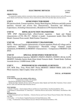
EC8252 ED NOTES FOR UNIT 1 & 2.pdf
1. EC8252 ELECTRONIC DEVICES L T P C
3 0 0 3
OBJECTIVES:
To acquaint the students with the construction, theory and operation of the basic electronic devices such as PN junction
diode, Bipolar and Field effect Transistors, Power control devices, LED, LCD and other Opto-electronic devices
UNIT I SEMICONDUCTOR DIODE 9
PN junction diode, Current equations, Energy Band diagram, Diffusion and drift current
densities, forward and reverse bias characteristics, Transition and Diffusion
Capacitances, Switching Characteristics, Breakdown in PN Junction Diodes.
UNIT II BIPOLAR JUNCTION TRANSISTORS 9
NPN -PNP -Operations-Early effect-Current equations – Input and Output
characteristics of CE, CB, CC - Hybrid -π model - h-parameter model, Ebers Moll
Model- Gummel Poon-model, Multi Emitter Transistor.
UNIT III FIELD EFFECT TRANSISTORS 9
JFETs – Drain and Transfer characteristics,-Current equations-Pinch off voltage and its
significance- MOSFET- Characteristics- Threshold voltage -Channel length
modulation, D-MOSFET, E-MOSFET- Characteristics – Comparison of MOSFET with
JFET.
UNIT IV SPECIAL SEMICONDUCTOR DEVICES 9
Metal-Semiconductor Junction- MESFET, FINFET, PINFET, CNTFET, DUAL GATE
MOSFET, Schottky barrier diode-Zener diode-Varactor diode –Tunnel diode- Gallium
Arsenide device, LASER diode, LDR.
UNIT V POWER DEVICES AND DISPLAY DEVICES 9
UJT, SCR, Diac, Triac, Power BJT- Power MOSFET- DMOS-VMOS. LED, LCD,
Photo transistor, Opto Coupler, Solar cell, CCD.
TOTAL : 45 PERIODS
OUTCOMES:
At the end of the course the students will be able to:
-I characteristic of diode, UJT and SCR
devices, LED, LCD and other Opto-electronic devices
TEXT BOOKS:
1. Donald A Neaman, ―Semiconductor Physics and Devices‖, Fourth Edition, Tata Mc GrawHill Inc. 2012.
2. Salivahanan. S, Suresh Kumar. N, Vallavaraj.A, ―Electronic Devices and circuits‖, Third Edition, Tata McGraw- Hill,
2008.
REFERENCES:
1. Robert Boylestad and Louis Nashelsky, ―Electron Devices and Circuit Theory‖ Pearson Prentice Hall, 10th edition,
July 2008.
2. R.S.Sedha, ― A Text Book of Applied Electronics‖ S.Chand Publications, 2006.
3. Yang, ―Fundamentals of Semiconductor devices‖, McGraw Hill International Edition, 1978.
2.
3.
4.
5.
6.
7.
8.
9.
10.
11.
12.
13.
14.
15.
16.
17.
18.
19.
20.
21.
22.
23.
24.
25.
26.
27.
28.
29.
30.
31.
32.
33.
34.
35.
36.
37.
38.
39.
40.
41.
42.
43.
44.
45.
46.
47.
48.
49.
50.
51.
52.
53.
54. UNIT II BIPOLAR JUNCTION
2.1 INTRODUCTION
The transistor is the main building block “element” of electronics. It is a semiconductor
device and it comes in two general types: the Bipolar Junction Transistor (BJT) and the Field
Effect Transistor (FET).
It is named as transistor which is an acronym of two terms: “transfer-of-resistor.” It means
that the internal resistance of transistor transfers from one value to another values depending on the
biasing voltage applied to the transistor. Thus it is called TRANSfer resISTOR: i.e.
TRANSISTOR.
A bipolar transistor (BJT) is a three terminal semiconductor device in which the operation
depends on the interaction of both majority and minority carriers and hence the name bipolar.
The voltage between two terminals controls the current through the third terminal. So it is
called current controlled device. This is the basic principle of the BJT
It can be used as amplifier and logic switches. BJT consists of three terminals:
• Collector : C
• Base : B
• Emitter : E
2.1.1 TYPES
There are two types of bipolar transistors
• NPN transistor and
• PNP transistor.
2.1.2 TRANSISTOR CONSTRUCTION
PNP Transistor: In PNP transistor a thin layer of N-type silicon is sandwiched between two layers
of P-type silicon.
NPN Transistor: In NPN transistor a thin layer of P-type silicon is sandwiched between two layers
of N-type silicon. The two types of BJT are represented in figure 2.1
Figure 2.1 Transistors: NPN, PNP