Download as PDF, PPTX
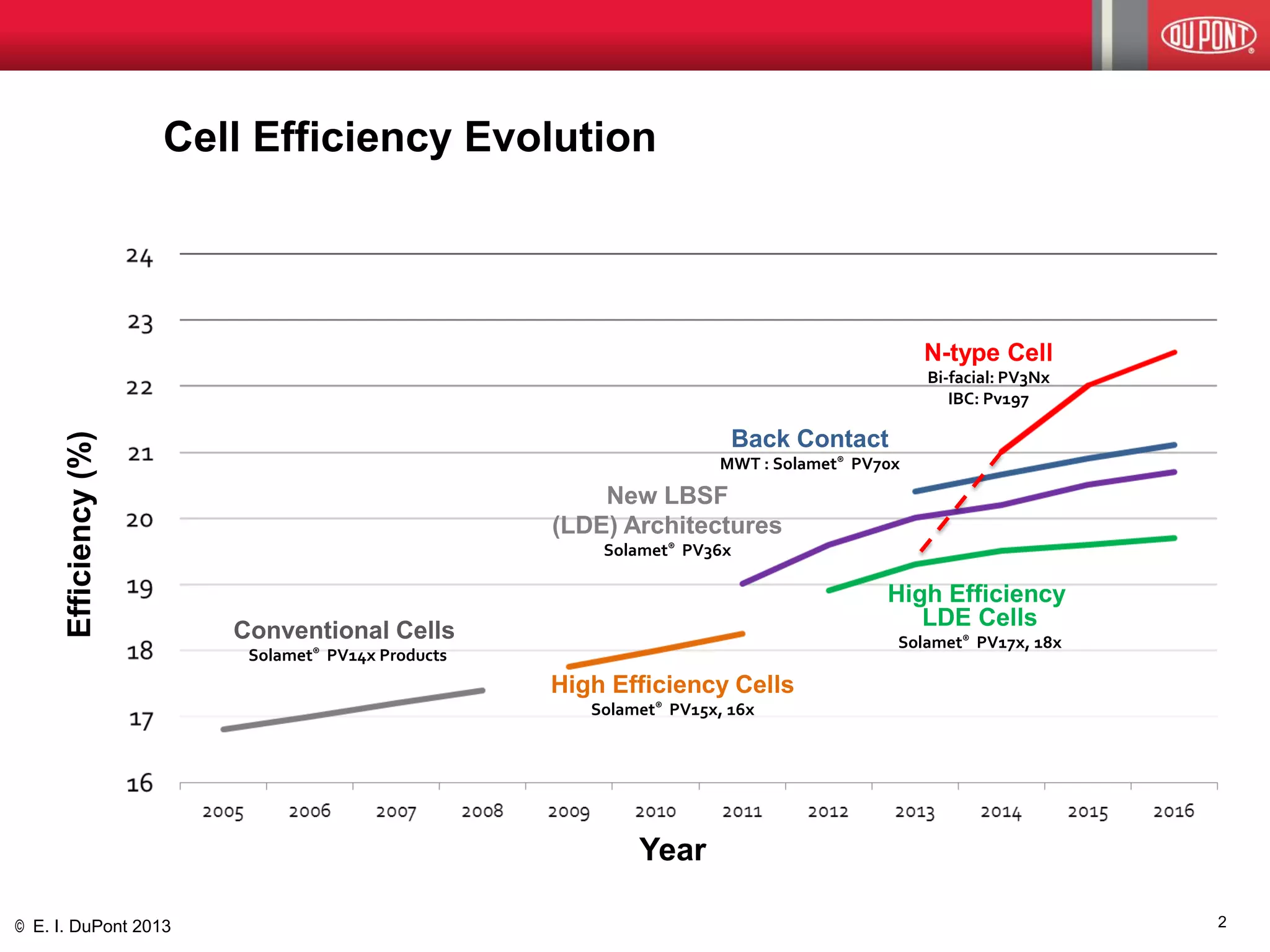
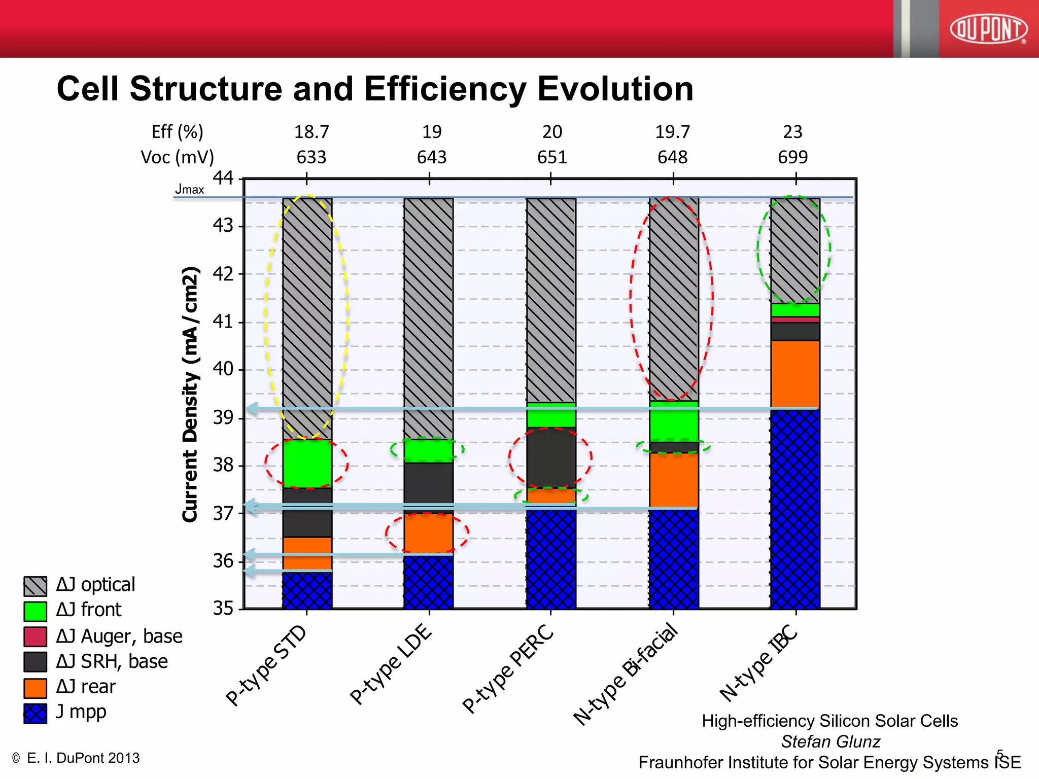
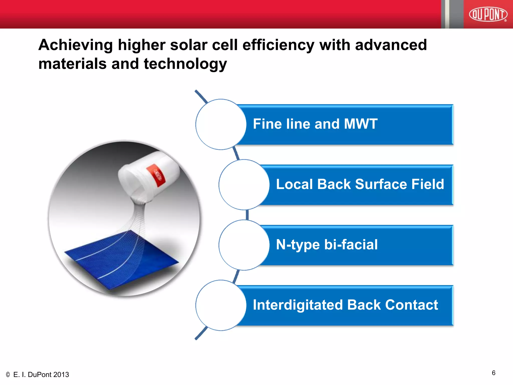
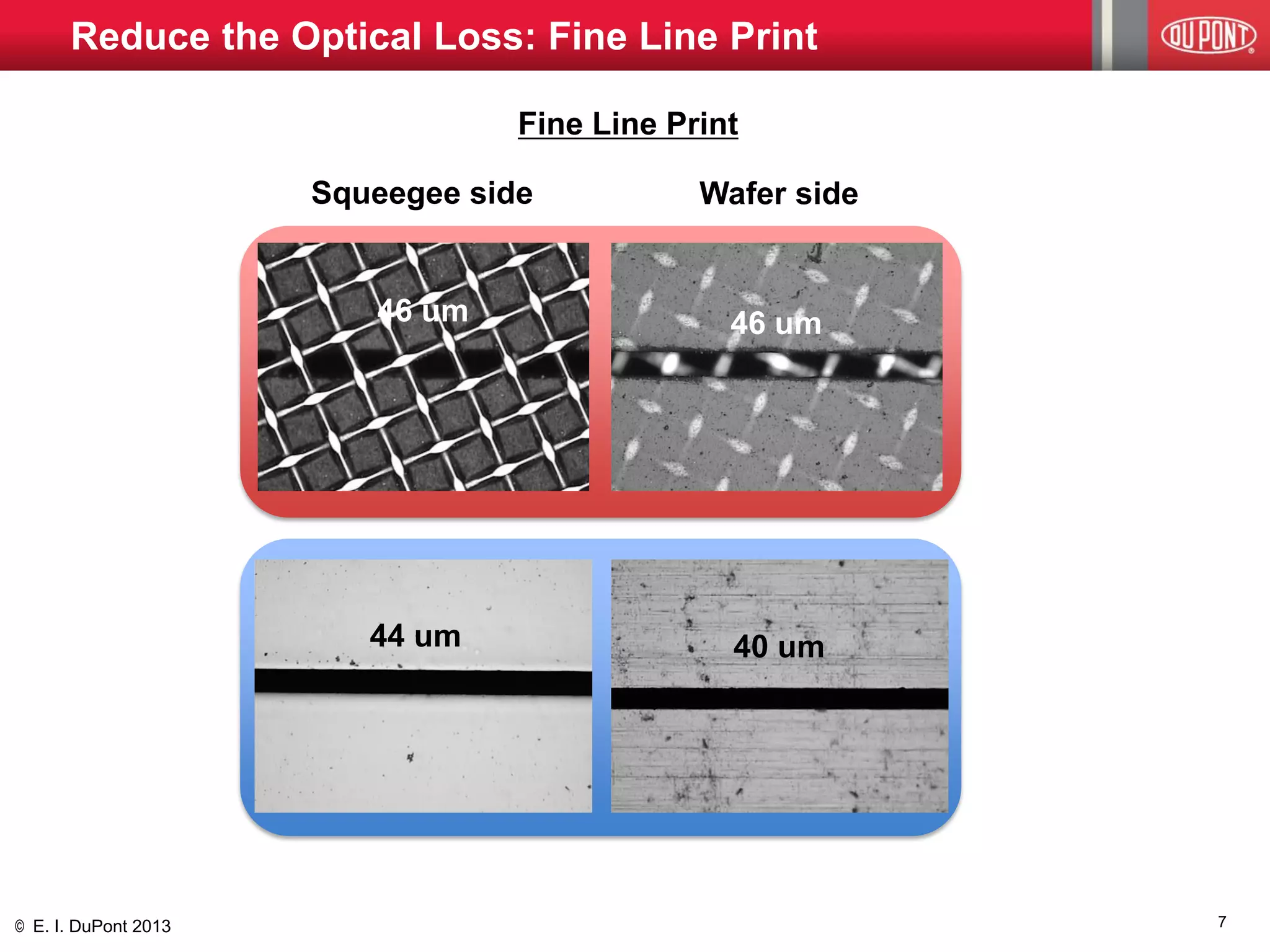
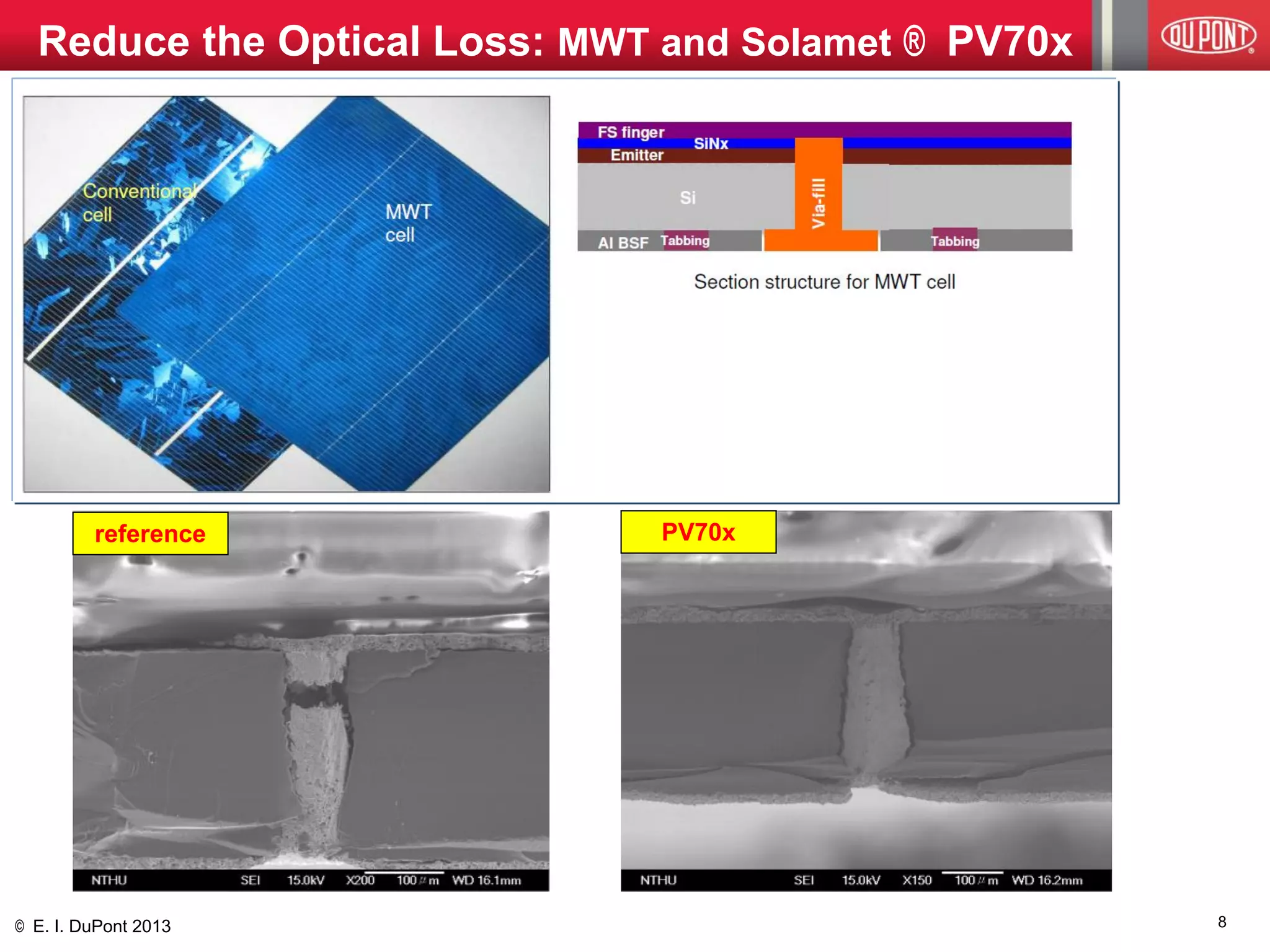
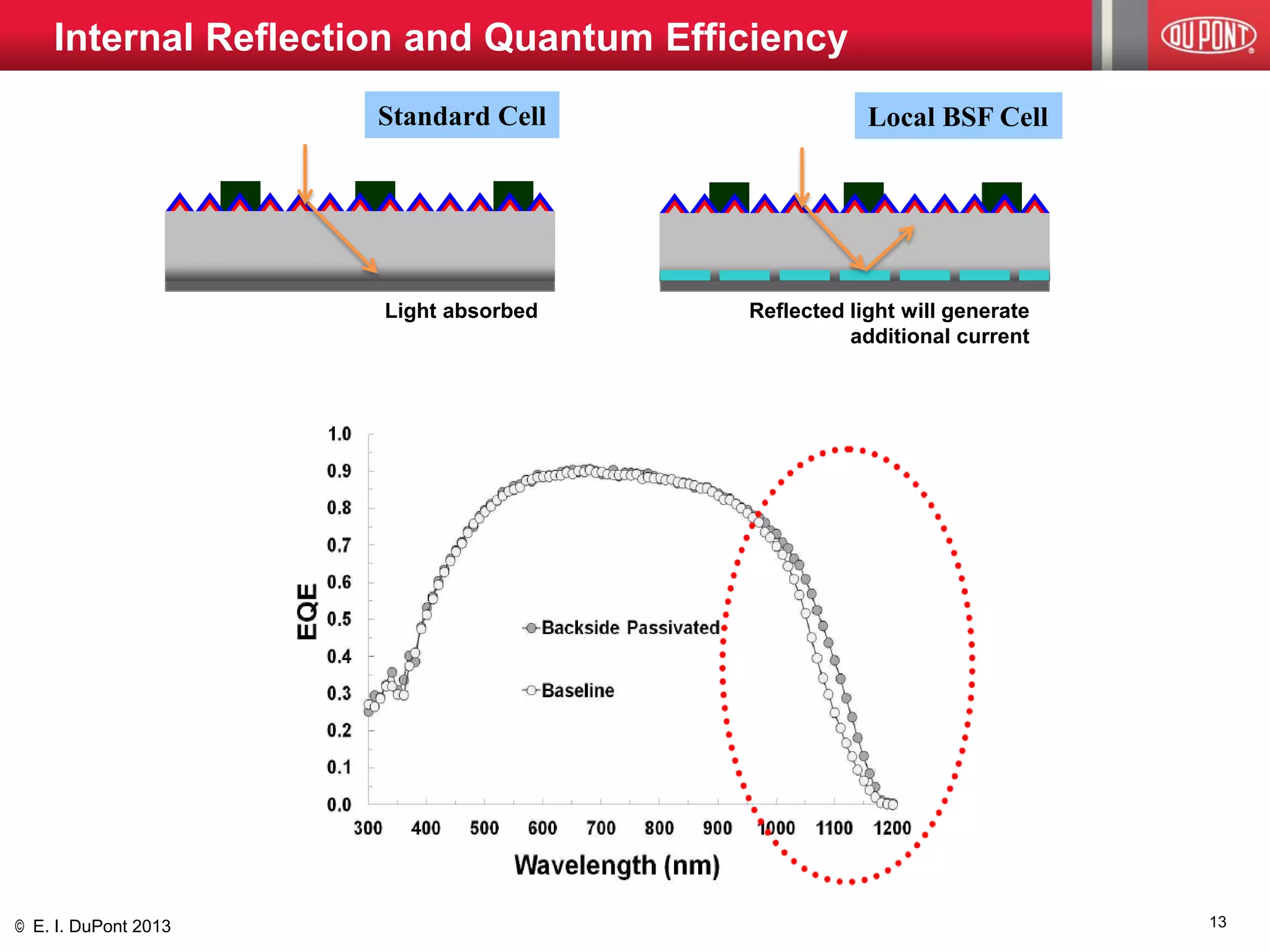
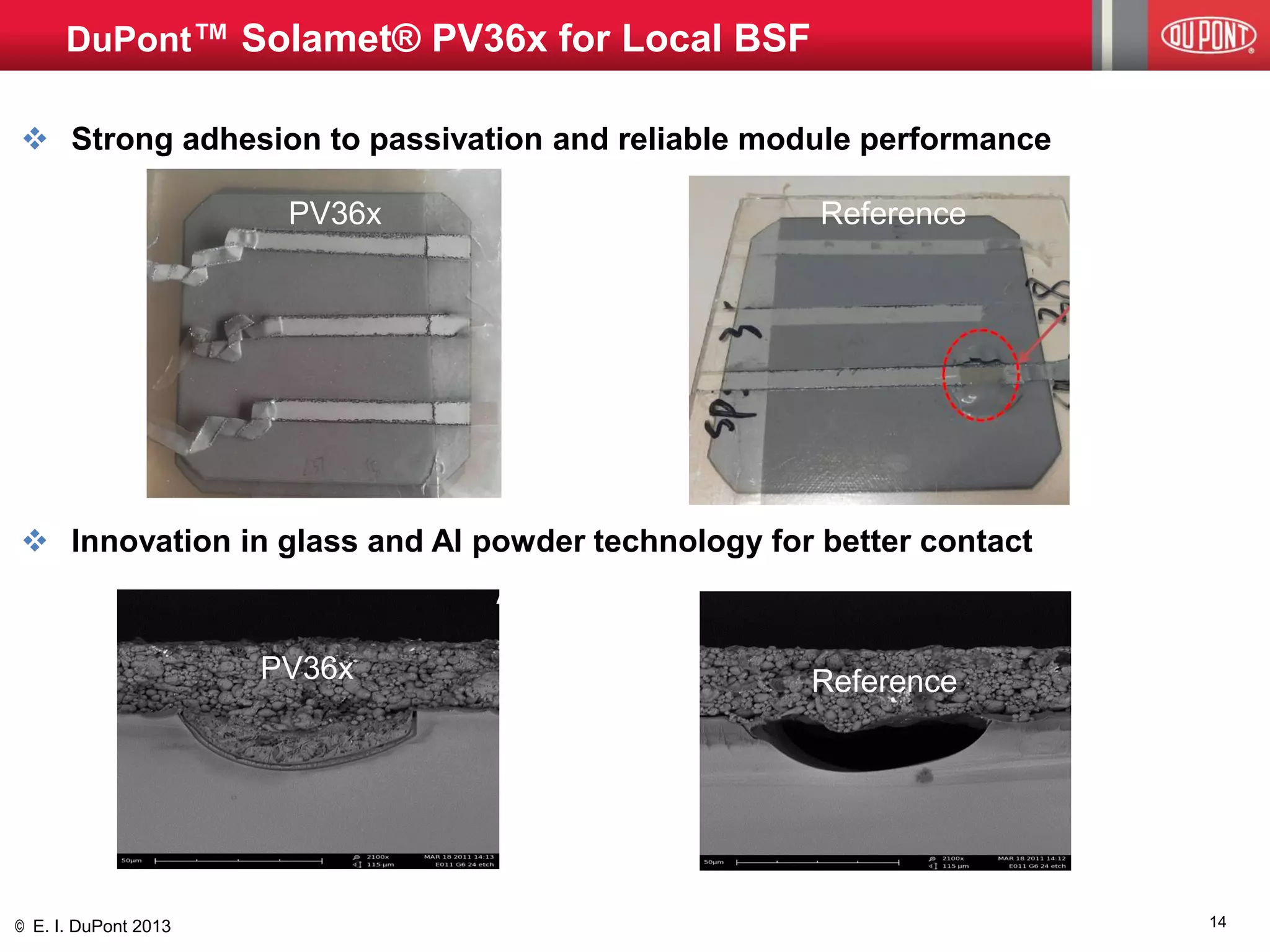
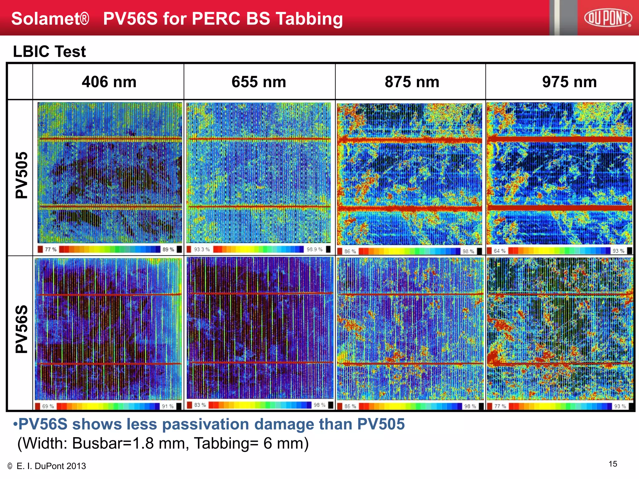
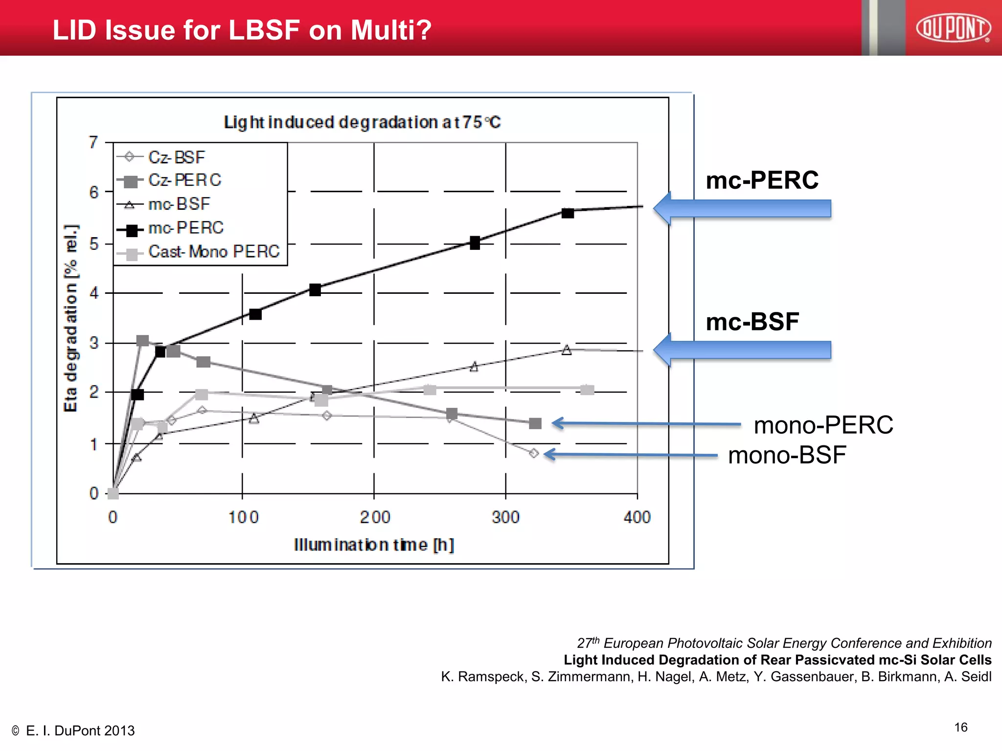
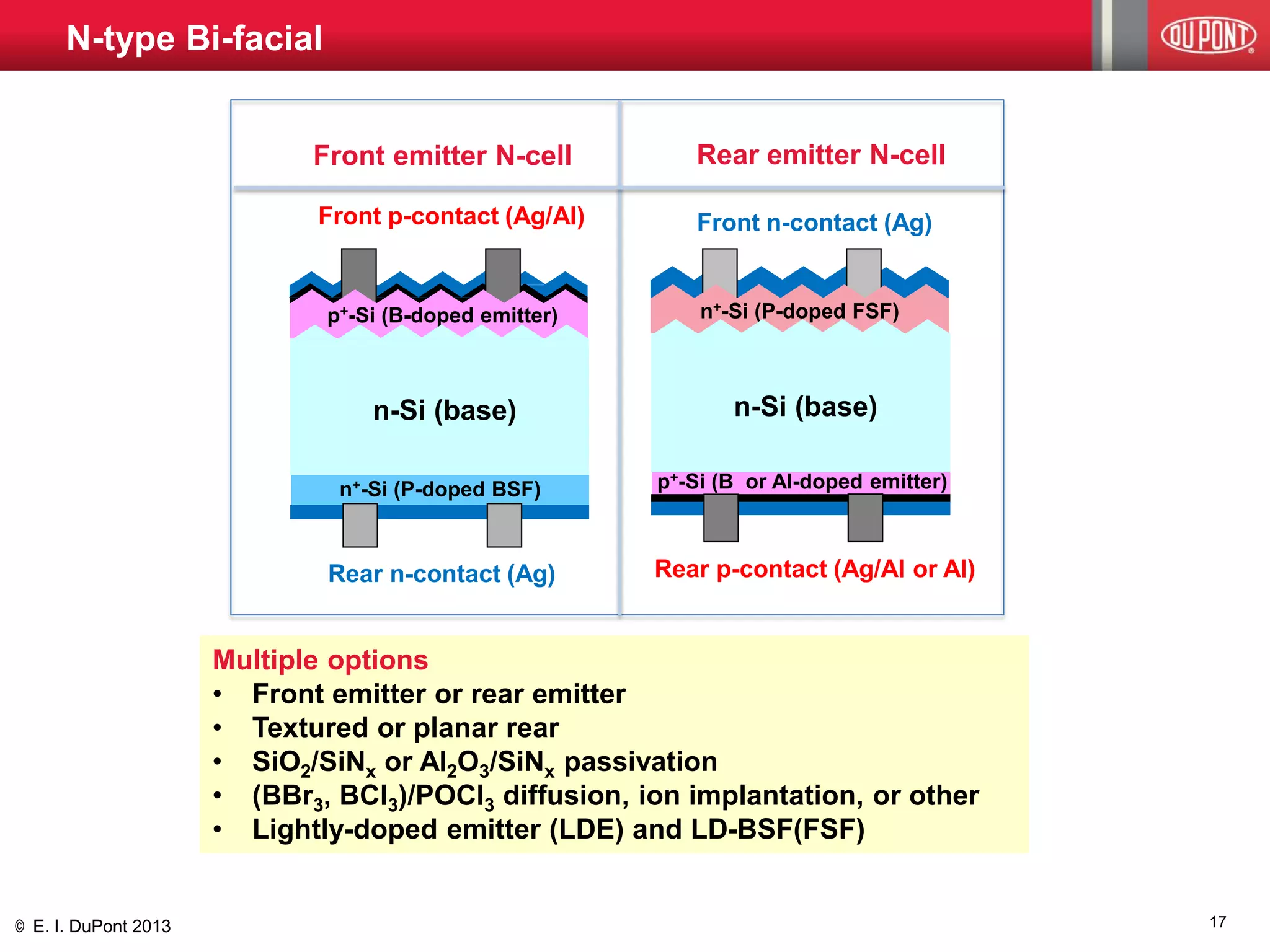
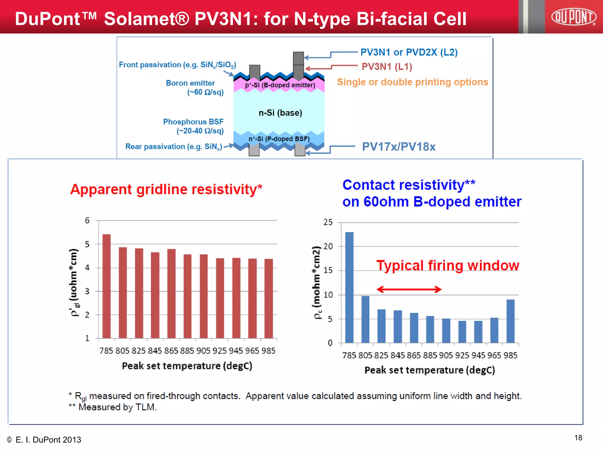
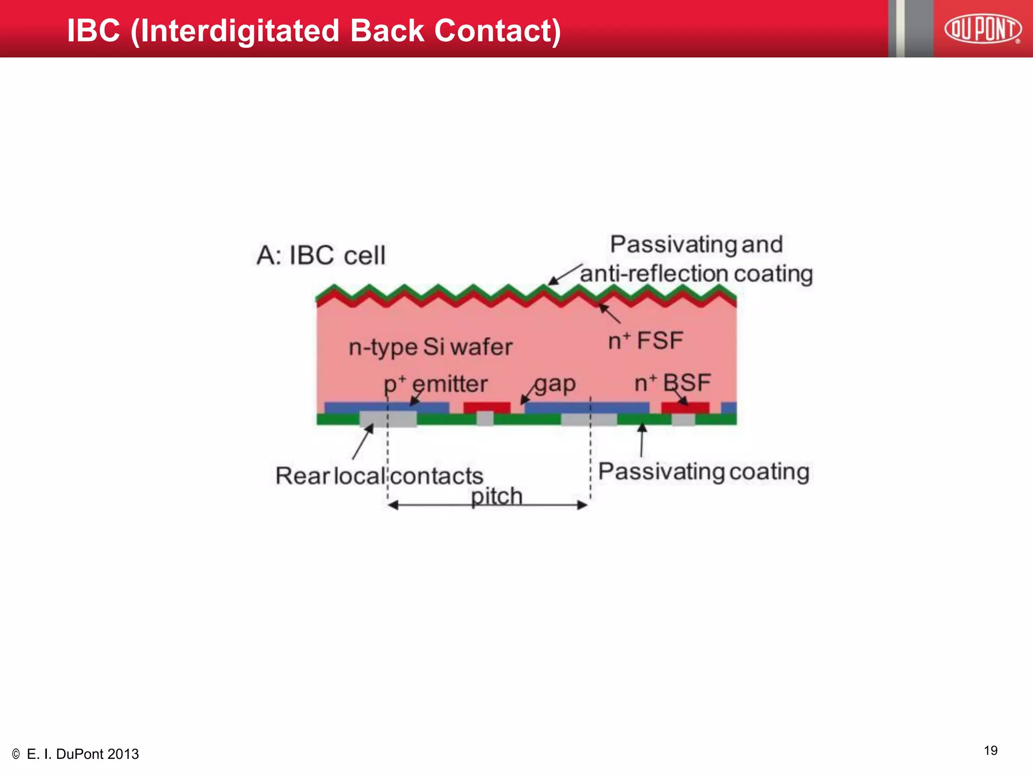
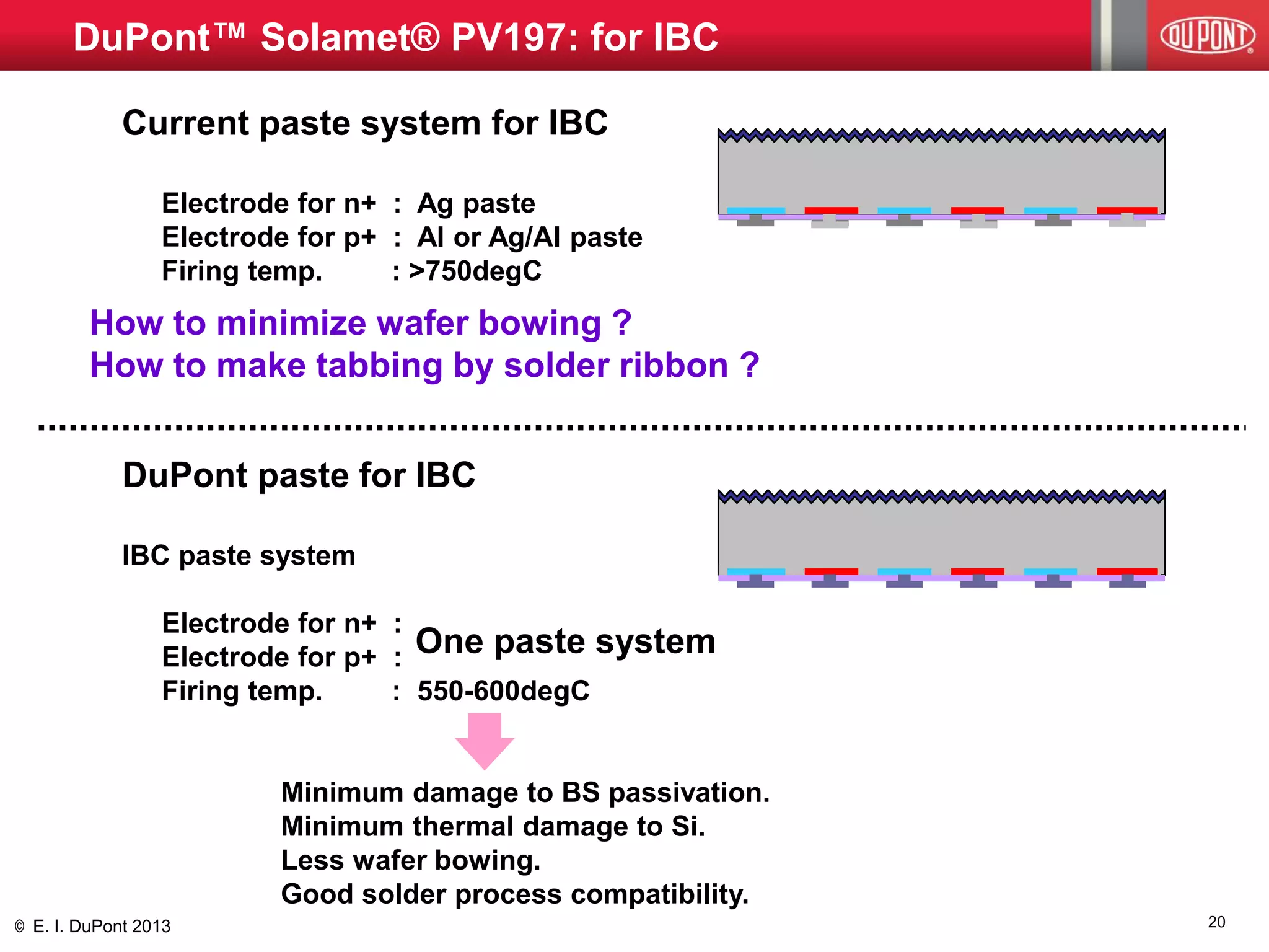
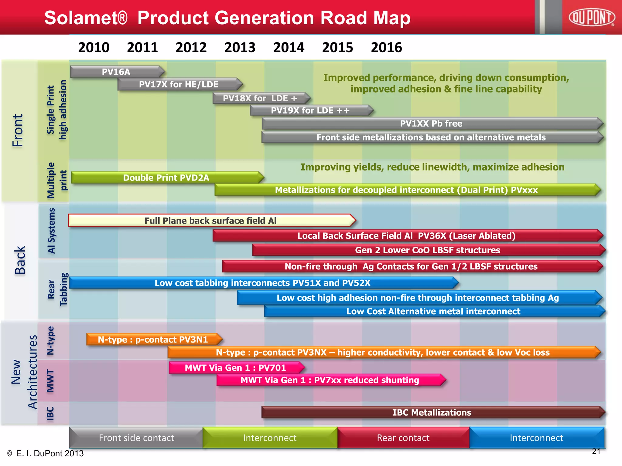

DuPont provides materials to enable higher efficiency solar cells through advanced technologies like interdigitated back contact, multi-wire, and n-type bi-facial cells. The presentation discusses DuPont products that can reduce optical and recombination losses to increase cell efficiency above 20%, such as fine line printing pastes and local back surface field pastes. It also reviews DuPont's roadmap to develop new materials to enable further efficiency increases through technologies like interdigitated back contact and multi-wire cells, with a goal of achieving 22% efficiency by 2015.


![Thin film and thin wafer PV: challenges for BIPV applications [PV 2009]](https://cdn.slidesharecdn.com/ss_thumbnails/skumanichpresentation-110805131834-phpapp01-thumbnail.jpg?width=640&height=640&fit=bounds)


