This document is the data sheet for Microchip's PIC12F629/675 8-bit microcontrollers. It provides detailed information on the memory organization, GPIO port, Timer0 and Timer1 modules, comparator module, analog-to-digital converter, data EEPROM, CPU features, instruction set, development support, electrical specifications, and packaging of these microcontrollers. The data sheet describes the various peripherals and features of the chips, their electrical characteristics, and is intended to provide engineers with the technical specifications needed to interface with and utilize the microcontrollers in their applications.


![PIC12F629/675
DS41190G-page 42 2010 Microchip Technology Inc.
REGISTER 6-2: VRCON: VOLTAGE REFERENCE CONTROL REGISTER (ADDRESS: 99h)
6.9 Comparator Interrupts
The comparator interrupt flag is set whenever there is
a change in the output value of the comparator.
Software will need to maintain information about the
status of the output bits, as read from CMCON<6>, to
determine the actual change that has occurred. The
CMIF bit, PIR1<3>, is the comparator interrupt flag.
This bit must be reset in software by clearing it to ‘0’.
Since it is also possible to write a ‘1’ to this register, a
simulated interrupt may be initiated.
The CMIE bit (PIE1<3>) and the PEIE bit (INT-
CON<6>) must be set to enable the interrupt. In addi-
tion, the GIE bit must also be set. If any of these bits are
cleared, the interrupt is not enabled, though the CMIF
bit will still be set if an interrupt condition occurs.
The user, in the Interrupt Service Routine, can clear the
interrupt in the following manner:
a) Any read or write of CMCON. This will end the
mismatch condition.
b) Clear flag bit CMIF.
A mismatch condition will continue to set flag bit CMIF.
Reading CMCON will end the mismatch condition, and
allow flag bit CMIF to be cleared.
TABLE 6-2: REGISTERS ASSOCIATED WITH COMPARATOR MODULE
R/W-0 U-0 R/W-0 R/W-0 R/W-0 R/W-0 R/W-0 R/W-0
VREN — VRR — VR3 VR2 VR1 VR0
bit 7 bit 0
Legend:
R = Readable bit W = Writable bit U = Unimplemented bit, read as ‘0’
-n = Value at POR ‘1’ = Bit is set ‘0’ = Bit is cleared x = Bit is unknown
bit 7 VREN: CVREF Enable bit
1 = CVREF circuit powered on
0 = CVREF circuit powered down, no IDD drain
bit 6 Unimplemented: Read as ‘0’
bit 5 VRR: CVREF Range Selection bit
1 = Low range
0 = High range
bit 4 Unimplemented: Read as ‘0’
bit 3-0 VR3:VR0: CVREF value selection 0 VR [3:0] 15
When VRR = 1: CVREF = (VR3:VR0 / 24) * VDD
When VRR = 0: CVREF = VDD/4 + (VR3:VR0 / 32) * VDD
Note: If a change in the CMCON register (COUT)
should occur when a read operation is
being executed (start of the Q2 cycle), then
the CMIF (PIR1<3>) interrupt flag may not
get set.
Address Name Bit 7 Bit 6 Bit 5 Bit 4 Bit 3 Bit 2 Bit 1 Bit 0
Value on
POR, BOD
Value on
all other
Resets
0Bh/8Bh INTCON GIE PEIE T0IE INTE GPIE T0IF INTF GPIF 0000 0000 0000 000u
0Ch PIR1 EEIF ADIF — — CMIF — — TMR1IF 00-- 0--0 00-- 0--0
19h CMCON — COUT — CINV CIS CM2 CM1 CM0 -0-0 0000 -0-0 0000
8Ch PIE1 EEIE ADIE — — CMIE — — TMR1IE 00-- 0--0 00-- 0--0
85h TRISIO — — TRISIO5 TRISIO4 TRISIO3 TRISIO2 TRISIO1 TRISIO0 --11 1111 --11 1111
99h VRCON VREN — VRR — VR3 VR2 VR1 VR0 0-0- 0000 0-0- 0000
Legend: x = unknown, u = unchanged, - = unimplemented, read as ‘0’. Shaded cells are not used by the comparator module.](https://image.slidesharecdn.com/675-150506082616-conversion-gate01/85/675-42-320.jpg)


![ 2010 Microchip Technology Inc. DS41190G-page 47
PIC12F629/675
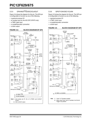
7.2 A/D Acquisition Requirements
For the A/D converter to meet its specified accuracy,
the charge holding capacitor (CHOLD) must be allowed
to fully charge to the input channel voltage level. The
analog input model is shown in Figure 7-3. The source
impedance (RS) and the internal sampling switch (RSS)
impedance directly affect the time required to charge
the capacitor CHOLD. The sampling switch (RSS)
impedance varies over the device voltage (VDD), see
Figure 7-3. The maximum recommended imped-
ance for analog sources is 10 k. As the impedance
is decreased, the acquisition time may be decreased.
After the analog input channel is selected (changed),
this acquisition must be done before the conversion
can be started.
To calculate the minimum acquisition time,
Equation 7-1 may be used. This equation assumes
that 1/2 LSb error is used (1024 steps for the A/D).
The 1/2 LSb error is the maximum error allowed for
the A/D to meet its specified resolution.
To calculate the minimum acquisition time, TACQ, see
the PIC®
Mid-Range Reference Manual (DS33023).
EQUATION 7-1: ACQUISITION TIME
FIGURE 7-3: ANALOG INPUT MODEL
TACQ
TC
TACQ
=
=
=
=
=
=
=
=
Amplifier Settling Time +
Hold Capacitor Charging Time +
Temperature Coefficient
TAMP + TC + TCOFF
2s + TC + [(Temperature -25°C)(0.05s/°C)]
CHOLD (RIC + RSS + RS) In(1/2047)
- 120pF (1k + 7k + 10k) In(0.0004885)
16.47s
2s + 16.47s + [(50°C -25C)(0.05s/C)
19.72s
Note 1: The reference voltage (VREF) has no effect on the equation, since it cancels itself out.
2: The charge holding capacitor (CHOLD) is not discharged after each conversion.
3: The maximum recommended impedance for analog sources is 10 k. This is required to meet the pin
leakage specification.
CPINVA
RS ANx
5 pF
VDD
VT = 0.6V
VT = 0.6V
I LEAKAGE
RIC 1K
Sampling
Switch
SS RSS
CHOLD
= DAC capacitance
VSS
6V
Sampling Switch
5V
4V
3V
2V
5 6 7 8 9 10 11
(k)
VDD
= 120 pF± 500 nA
Legend: CPIN
VT
I LEAKAGE
RIC
SS
CHOLD
= input capacitance
= threshold voltage
= leakage current at the pin due to
= interconnect resistance
= sampling switch
= sample/hold capacitance (from DAC)
various junctions](https://image.slidesharecdn.com/675-150506082616-conversion-gate01/85/675-47-320.jpg)


![ 2010 Microchip Technology Inc. DS41190G-page 73
PIC12F629/675
10.2 Instruction Descriptions
ADDLW Add Literal and W
Syntax: [label] ADDLW k
Operands: 0 k 255
Operation: (W) + k (W)
Status Affected: C, DC, Z
Description: The contents of the W register
are added to the eight-bit literal ‘k’
and the result is placed in the W
register.
ADDWF Add W and f
Syntax: [label] ADDWF f,d
Operands: 0 f 127
d
Operation: (W) + (f) (destination)
Status Affected: C, DC, Z
Description: Add the contents of the W register
with register ‘f’. If ‘d’ is 0, the
result is stored in the W register. If
‘d’ is 1, the result is stored back in
register ‘f’.
ANDLW AND Literal with W
Syntax: [label] ANDLW k
Operands: 0 k 255
Operation: (W) .AND. (k) (W)
Status Affected: Z
Description: The contents of W register are
AND’ed with the eight-bit literal
‘k’. The result is placed in the W
register.
ANDWF AND W with f
Syntax: [label] ANDWF f,d
Operands: 0 f 127
d
Operation: (W) .AND. (f) (destination)
Status Affected: Z
Description: AND the W register with register
‘f’. If ‘d’ is 0, the result is stored in
the W register. If ‘d’ is 1, the result
is stored back in register ‘f’.
BCF Bit Clear f
Syntax: [label] BCF f,b
Operands: 0 f 127
0 b 7
Operation: 0 (f<b>)
Status Affected: None
Description: Bit ‘b’ in register ‘f’ is cleared.
BSF Bit Set f
Syntax: [label] BSF f,b
Operands: 0 f 127
0 b 7
Operation: 1 (f<b>)
Status Affected: None
Description: Bit ‘b’ in register ‘f’ is set.
BTFSS Bit Test f, Skip if Set
Syntax: [label] BTFSS f,b
Operands: 0 f 127
0 b < 7
Operation: skip if (f<b>) = 1
Status Affected: None
Description: If bit ‘b’ in register ‘f’ is ‘0’, the next
instruction is executed.
If bit ‘b’ is ‘1’, then the next
instruction is discarded and a NOP
is executed instead, making this a
2TCY instruction.](https://image.slidesharecdn.com/675-150506082616-conversion-gate01/85/675-73-320.jpg)
![PIC12F629/675
DS41190G-page 74 2010 Microchip Technology Inc.
BTFSC Bit Test, Skip if Clear
Syntax: [label] BTFSC f,b
Operands: 0 f 127
0 b 7
Operation: skip if (f<b>) = 0
Status Affected: None
Description: If bit ‘b’ in register ‘f’ is ‘1’, the next
instruction is executed.
If bit ‘b’, in register ‘f’, is ‘0’, the
next instruction is discarded, and
a NOP is executed instead, making
this a 2TCY instruction.
CALL Call Subroutine
Syntax: [ label ] CALL k
Operands: 0 k 2047
Operation: (PC)+ 1 TOS,
k PC<10:0>,
(PCLATH<4:3>) PC<12:11>
Status Affected: None
Description: Call Subroutine. First, return
address (PC + 1) is pushed onto
the stack. The eleven-bit immedi-
ate address is loaded into PC bits
<10:0>. The upper bits of the PC
are loaded from PCLATH. CALL is
a two-cycle instruction.
CLRF Clear f
Syntax: [label] CLRF f
Operands: 0 f 127
Operation: 00h (f)
1 Z
Status Affected: Z
Description: The contents of register ‘f’ are
cleared and the Z bit is set.
CLRW Clear W
Syntax: [ label ] CLRW
Operands: None
Operation: 00h (W)
1 Z
Status Affected: Z
Description: W register is cleared. Zero bit (Z)
is set.
CLRWDT Clear Watchdog Timer
Syntax: [ label ] CLRWDT
Operands: None
Operation: 00h WDT
0 WDT prescaler,
1 TO
1 PD
Status Affected: TO, PD
Description: CLRWDT instruction resets the
Watchdog Timer. It also resets the
prescaler of the WDT.
Status bits TO and PD are set.
COMF Complement f
Syntax: [ label ] COMF f,d
Operands: 0 f 127
d [0,1]
Operation: (f) (destination)
Status Affected: Z
Description: The contents of register ‘f’ are
complemented. If ‘d’ is 0, the
result is stored in W. If ‘d’ is 1, the
result is stored back in register ‘f’.
DECF Decrement f
Syntax: [label] DECF f,d
Operands: 0 f 127
d [0,1]
Operation: (f) - 1 (destination)
Status Affected: Z
Description: Decrement register ‘f’. If ‘d’ is 0,
the result is stored in the W
register. If ‘d’ is 1, the result is
stored back in register ‘f’.](https://image.slidesharecdn.com/675-150506082616-conversion-gate01/85/675-74-320.jpg)
![ 2010 Microchip Technology Inc. DS41190G-page 75
PIC12F629/675
DECFSZ Decrement f, Skip if 0
Syntax: [ label ] DECFSZ f,d
Operands: 0 f 127
d [0,1]
Operation: (f) - 1 (destination);
skip if result = 0
Status Affected: None
Description: The contents of register ‘f’ are
decremented. If ‘d’ is 0, the result
is placed in the W register. If ‘d’ is
1, the result is placed back in
register ‘f’.
If the result is 1, the next instruc-
tion is executed. If the result is 0,
then a NOP is executed instead,
making it a 2TCY instruction.
GOTO Unconditional Branch
Syntax: [ label ] GOTO k
Operands: 0 k 2047
Operation: k PC<10:0>
PCLATH<4:3> PC<12:11>
Status Affected: None
Description: GOTO is an unconditional branch.
The eleven-bit immediate value is
loaded into PC bits <10:0>. The
upper bits of PC are loaded from
PCLATH<4:3>. GOTO is a two-
cycle instruction.
INCF Increment f
Syntax: [ label ] INCF f,d
Operands: 0 f 127
d [0,1]
Operation: (f) + 1 (destination)
Status Affected: Z
Description: The contents of register ‘f’ are
incremented. If ‘d’ is 0, the result
is placed in the W register. If ‘d’ is
1, the result is placed back in
register ‘f’.
INCFSZ Increment f, Skip if 0
Syntax: [ label ] INCFSZ f,d
Operands: 0 f 127
d [0,1]
Operation: (f) + 1 (destination),
skip if result = 0
Status Affected: None
Description: The contents of register ‘f’ are
incremented. If ‘d’ is 0, the result
is placed in the W register. If ‘d’ is
1, the result is placed back in
register ‘f’.
If the result is 1, the next instruc-
tion is executed. If the result is 0,
a NOP is executed instead, making
it a 2TCY instruction.
IORLW Inclusive OR Literal with W
Syntax: [ label ] IORLW k
Operands: 0 k 255
Operation: (W) .OR. k (W)
Status Affected: Z
Description: The contents of the W register are
OR’ed with the eight-bit literal ‘k’.
The result is placed in the W
register.
IORWF Inclusive OR W with f
Syntax: [ label ] IORWF f,d
Operands: 0 f 127
d [0,1]
Operation: (W) .OR. (f) (destination)
Status Affected: Z
Description: Inclusive OR the W register with
register ‘f’. If ‘d’ is 0, the result is
placed in the W register. If ‘d’ is 1,
the result is placed back in
register ‘f’.](https://image.slidesharecdn.com/675-150506082616-conversion-gate01/85/675-75-320.jpg)
![PIC12F629/675
DS41190G-page 76 2010 Microchip Technology Inc.
MOVF Move f
Syntax: [ label ] MOVF f,d
Operands: 0 f 127
d [0,1]
Operation: (f) (dest)
Status Affected: Z
Description: The contents of register f is
moved to a destination dependent
upon the status of d. If d = 0,
the destination is W register. If d =
1, the destination is file register f
itself. d = 1 is useful to test a file
register since status flag Z is
affected.
Words: 1
Cycles: 1
Example: MOVF FSR, 0
After Instruction
W = value in FSR
register
Z = 1
MOVLW Move literal to W
Syntax: [ label ] MOVLW k
Operands: 0 k 255
Operation: k (W)
Status Affected: None
Description: The eight-bit literal ‘k’ is loaded into
W register. The “don’t cares” will
assemble as ‘0’s.
Words: 1
Cycles: 1
Example: MOVLW 0x5A
After Instruction
W = 0x5A
MOVWF Move W to f
Syntax: [ label ] MOVWF f
Operands: 0 f 127
Operation: (W) (f)
Status Affected: None
Description: Move data from W register to
register ‘f’.
Words: 1
Cycles: 1
Example: MOVWF OPTION
Before Instruction
OPTION = 0xFF
W = 0x4F
After Instruction
OPTION = 0x4F
W = 0x4F
NOP No Operation
Syntax: [ label ] NOP
Operands: None
Operation: No operation
Status Affected: None
Description: No operation.
Words: 1
Cycles: 1
Example: NOP](https://image.slidesharecdn.com/675-150506082616-conversion-gate01/85/675-76-320.jpg)
![ 2010 Microchip Technology Inc. DS41190G-page 77
PIC12F629/675
RETFIE Return from Interrupt
Syntax: [ label ] RETFIE
Operands: None
Operation: TOS PC,
1 GIE
Status Affected: None
Description: Return from Interrupt. Stack is
POPed and Top-of-Stack (TOS) is
loaded in the PC. Interrupts are
enabled by setting Global
Interrupt Enable bit, GIE
(INTCON<7>). This is a two-cycle
instruction.
Words: 1
Cycles: 2
Example: RETFIE
After Interrupt
PC = TOS
GIE = 1
RETLW Return with literal in W
Syntax: [ label ] RETLW k
Operands: 0 k 255
Operation: k (W);
TOS PC
Status Affected: None
Description: The W register is loaded with the
eight-bit literal ‘k’. The program
counter is loaded from the top of
the stack (the return address).
This is a two-cycle instruction.
Words: 1
Cycles: 2
Example:
TABLE
CALL TABLE;W contains
table
;offset value
• ;W now has table value
•
•
ADDWF PCL ;W = offset
RETLW k1 ;Begin table
RETLW k2 ;
•
•
•
RETLW kn ; End of table
Before Instruction
W = 0x07
After Instruction
W = value of k8
RETURN Return from Subroutine
Syntax: [ label ] RETURN
Operands: None
Operation: TOS PC
Status Affected: None
Description: Return from subroutine. The stack
is POPed and the top of the stack
(TOS) is loaded into the program
counter. This is a two-cycle
instruction.](https://image.slidesharecdn.com/675-150506082616-conversion-gate01/85/675-77-320.jpg)
![PIC12F629/675
DS41190G-page 78 2010 Microchip Technology Inc.
RLF Rotate Left f through Carry
Syntax: [ label ] RLF f,d
Operands: 0 f 127
d [0,1]
Operation: See description below
Status Affected: C
Description: The contents of register ‘f’ are rotated
one bit to the left through the Carry
Flag. If ‘d’ is 0, the result is placed in
the W register. If ‘d’ is 1, the result is
stored back in register ‘f’.
RRF Rotate Right f through Carry
Syntax: [ label ] RRF f,d
Operands: 0 f 127
d [0,1]
Operation: See description below
Status Affected: C
Description: The contents of register ‘f’ are
rotated one bit to the right through
the Carry Flag. If ‘d’ is 0, the result
is placed in the W register. If ‘d’ is
1, the result is placed back in
register ‘f’.
SLEEP
Syntax: [ label ] SLEEP
Operands: None
Operation: 00h WDT,
0 WDT prescaler,
1 TO,
0 PD
Status Affected: TO, PD
Description: The power-down Status bit, PD is
cleared. Time-out Status bit, TO
is set. Watchdog Timer and its
prescaler are cleared.
The processor is put into Sleep
mode with the oscillator stopped.
Register fC
Register fC
SUBLW Subtract W from Literal
Syntax: [ label ] SUBLW k
Operands: 0 k 255
Operation: k - (W) W)
Status Affected: C, DC, Z
Description: The W register is subtracted (2’s
complement method) from the
eight-bit literal ‘k’. The result is
placed in the W register.
SUBWF Subtract W from f
Syntax: [ label ] SUBWF f,d
Operands: 0 f 127
d [0,1]
Operation: (f) - (W) destination)
Status
Affected:
C, DC, Z
Description: Subtract (2’s complement method)
W register from register ‘f’. If ‘d’ is
0, the result is stored in the W
register. If ‘d’ is 1, the result is
stored back in register ‘f’.
SWAPF Swap Nibbles in f
Syntax: [ label ] SWAPF f,d
Operands: 0 f 127
d [0,1]
Operation: (f<3:0>) (destination<7:4>),
(f<7:4>) (destination<3:0>)
Status Affected: None
Description: The upper and lower nibbles of
register ‘f’ are exchanged. If ‘d’ is
0, the result is placed in the W
register. If ‘d’ is 1, the result is
placed in register ‘f’.](https://image.slidesharecdn.com/675-150506082616-conversion-gate01/85/675-78-320.jpg)
![ 2010 Microchip Technology Inc. DS41190G-page 79
PIC12F629/675
XORLW Exclusive OR Literal with W
Syntax: [label] XORLW k
Operands: 0 k 255
Operation: (W) .XOR. k W)
Status Affected: Z
Description: The contents of the W register
are XOR’ed with the eight-bit
literal ‘k’. The result is placed in
the W register.
XORWF Exclusive OR W with f
Syntax: [label] XORWF f,d
Operands: 0 f 127
d [0,1]
Operation: (W) .XOR. (f) destination)
Status Affected: Z
Description: Exclusive OR the contents of the
W register with register ‘f’. If ‘d’ is
0, the result is stored in the W
register. If ‘d’ is 1, the result is
stored back in register ‘f’.](https://image.slidesharecdn.com/675-150506082616-conversion-gate01/85/675-79-320.jpg)


![ 2010 Microchip Technology Inc. DS41190G-page 123
PIC12F629/675
8-Lead Plastic Dual Flat, No Lead Package (MD) – 4x4x0.9 mm Body [DFN]
Note: For the most current package drawings, please see the Microchip Packaging Specification located at
http://www.microchip.com/packaging
Microchip Technology Drawing C04-131E Sheet 1 of 2](https://image.slidesharecdn.com/675-150506082616-conversion-gate01/85/675-128-320.jpg)
![PIC12F629/675
DS41190G-page 124 2010 Microchip Technology Inc.
8-Lead Plastic Dual Flat, No Lead Package (MD) – 4x4x0.9 mm Body [DFN]
Note: For the most current package drawings, please see the Microchip Packaging Specification located at
http://www.microchip.com/packaging
Microchip Technology Drawing C04-131E Sheet 2 of 2](https://image.slidesharecdn.com/675-150506082616-conversion-gate01/85/675-129-320.jpg)