Download as PDF, PPTX
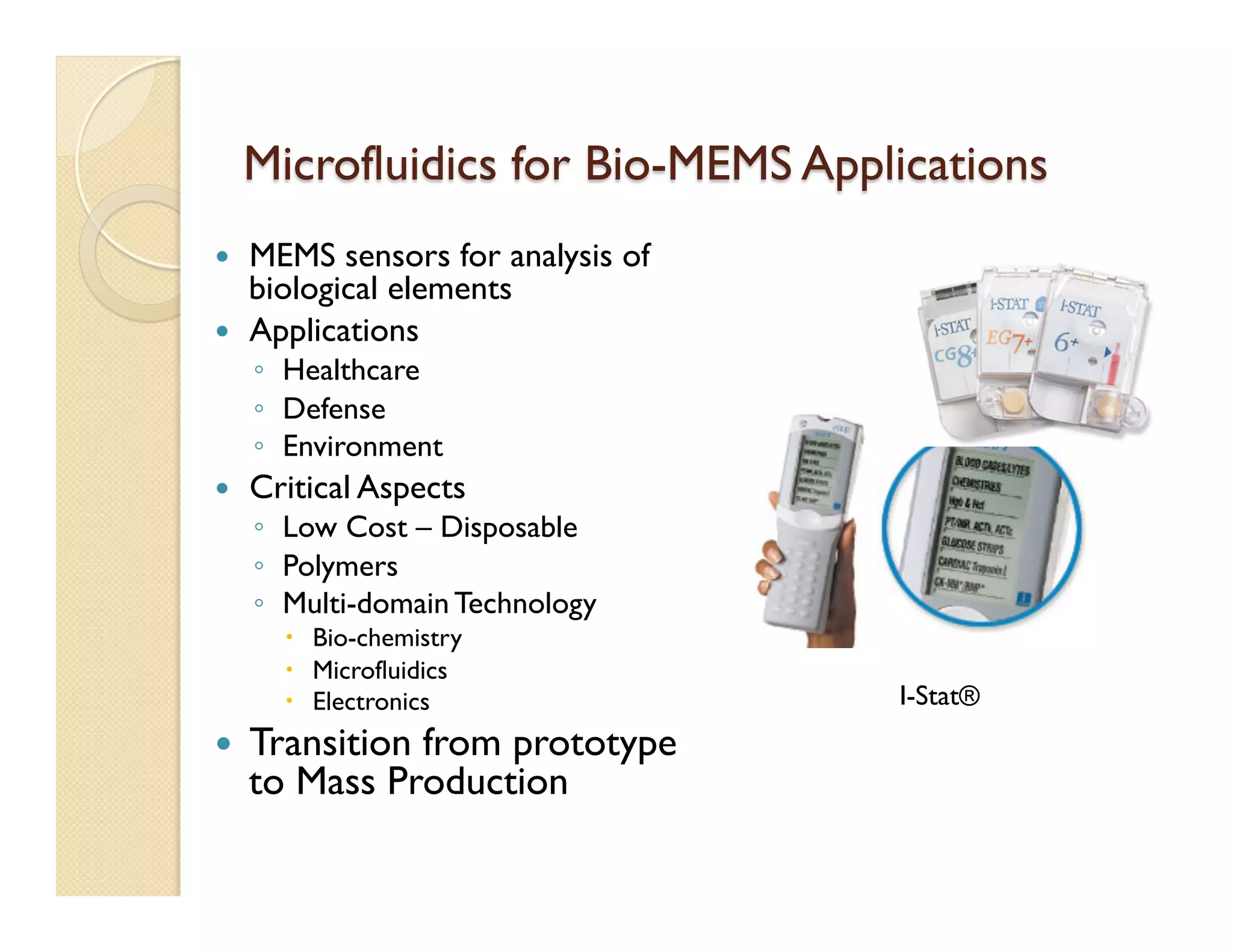
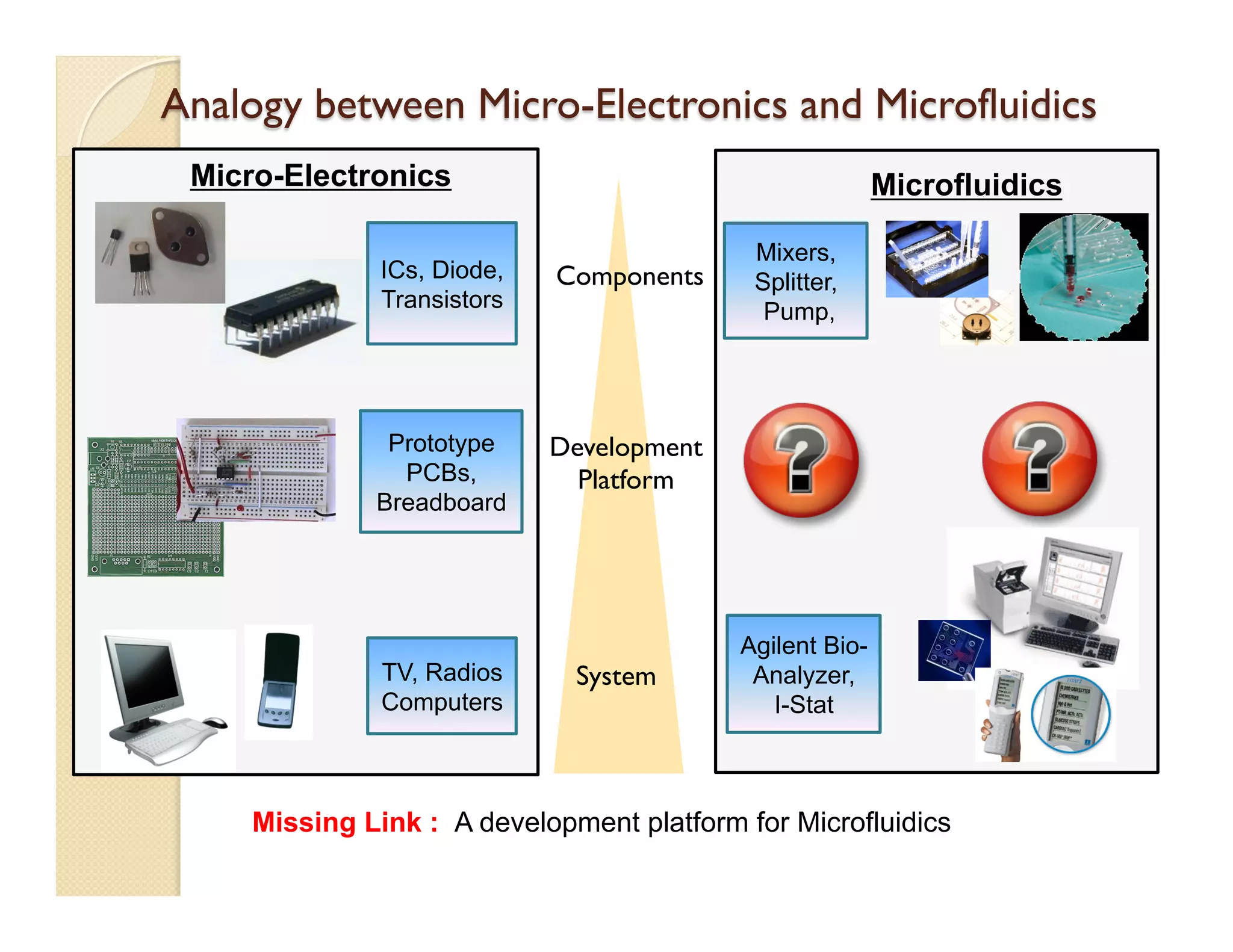
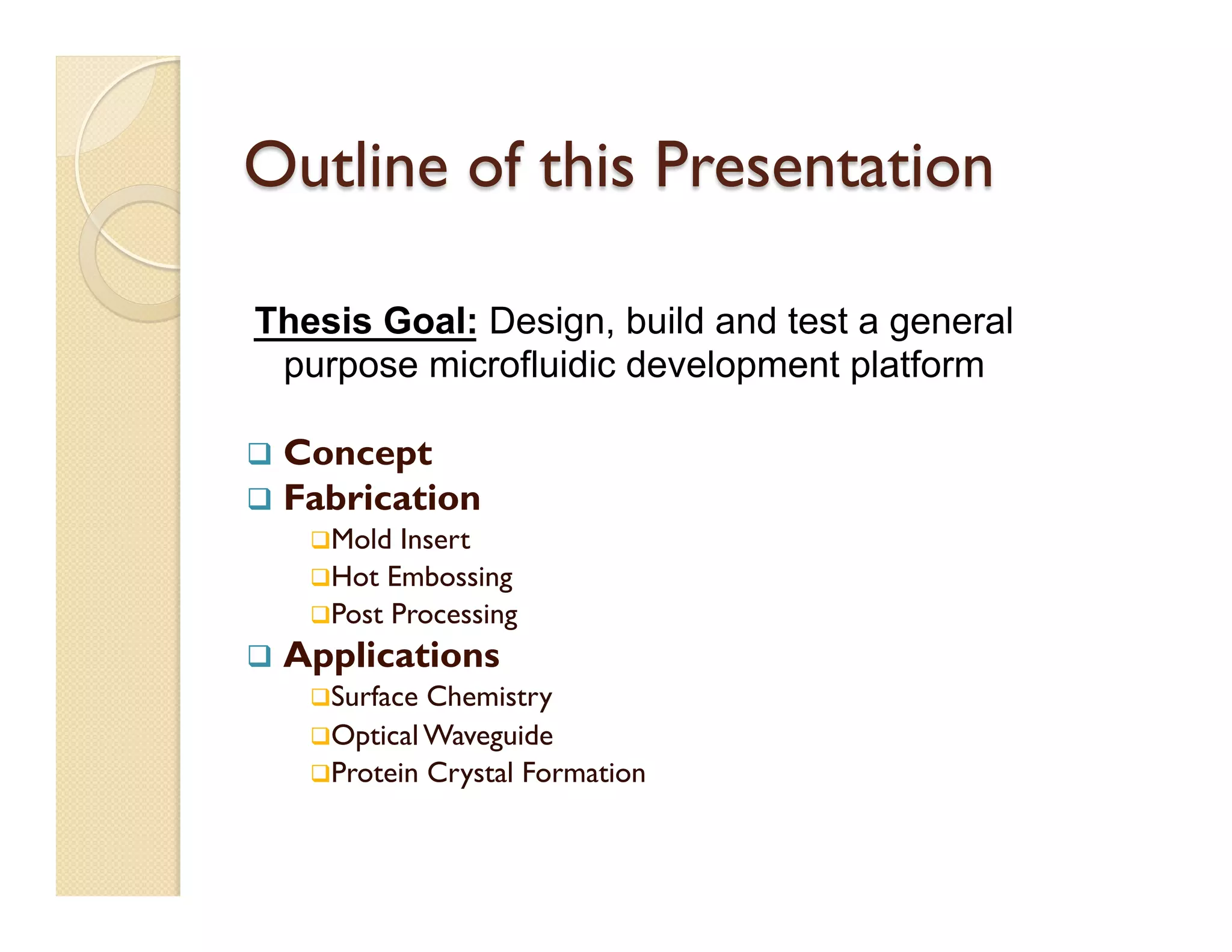
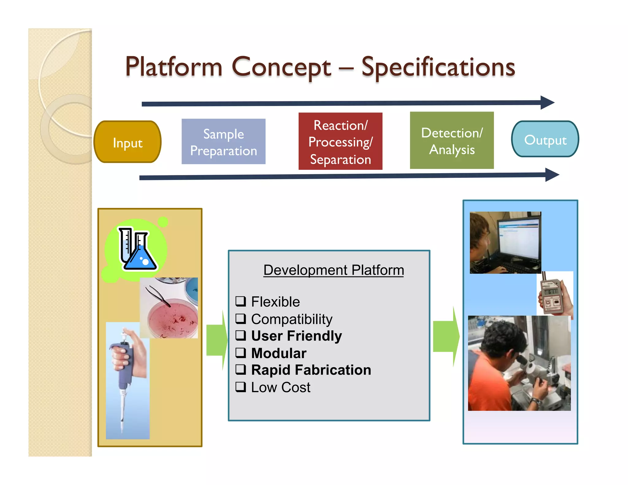
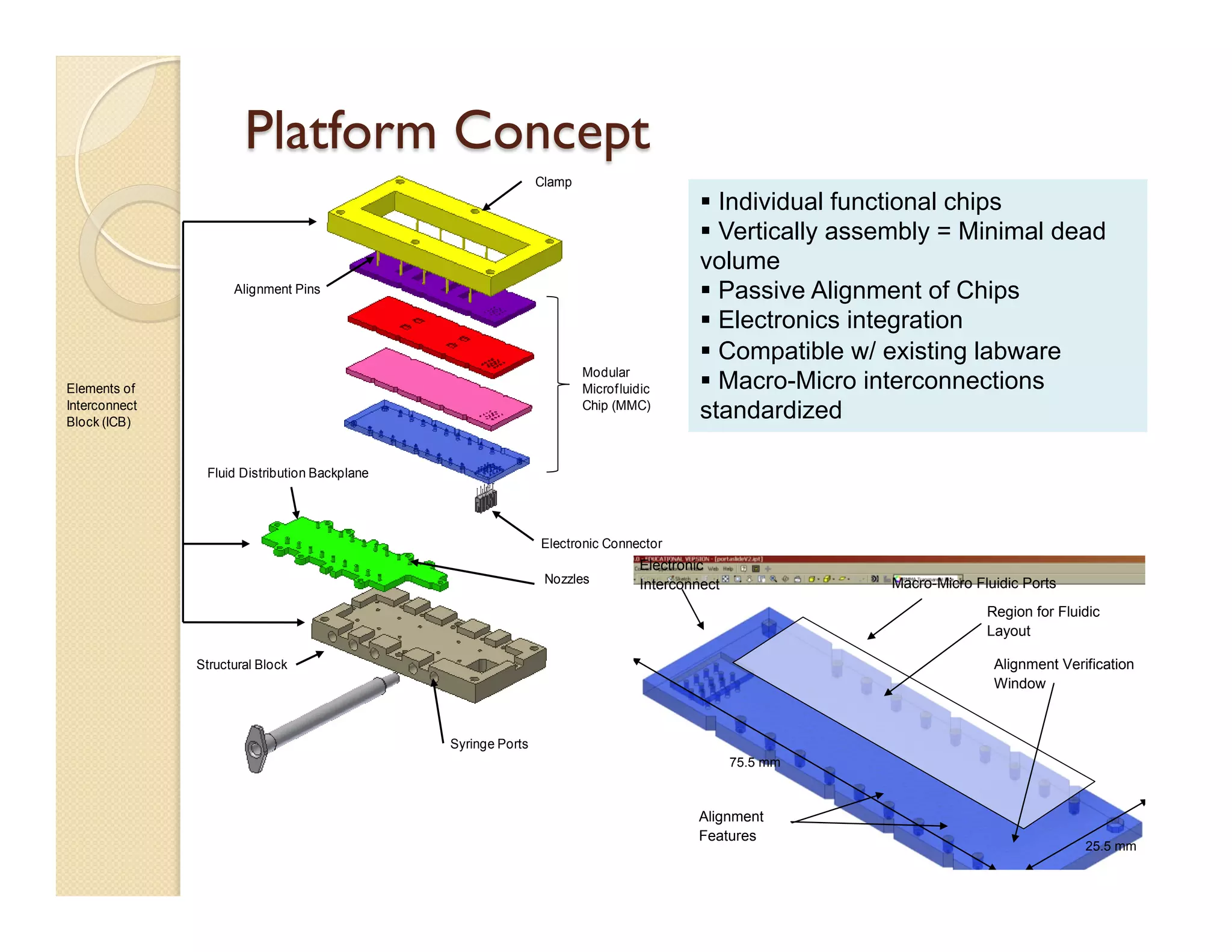
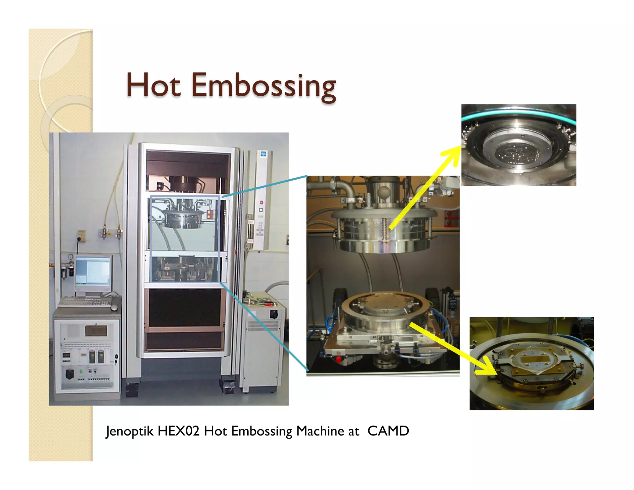
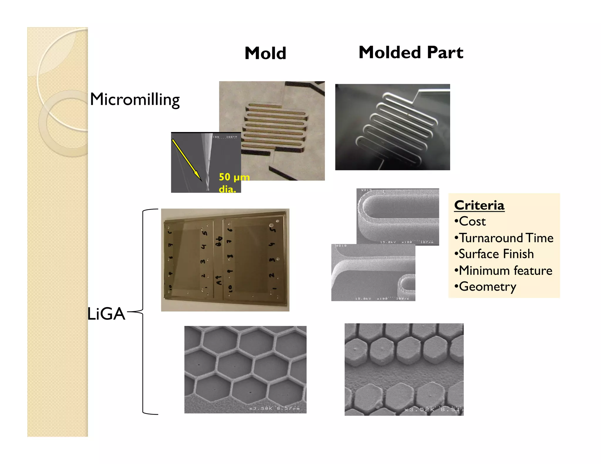
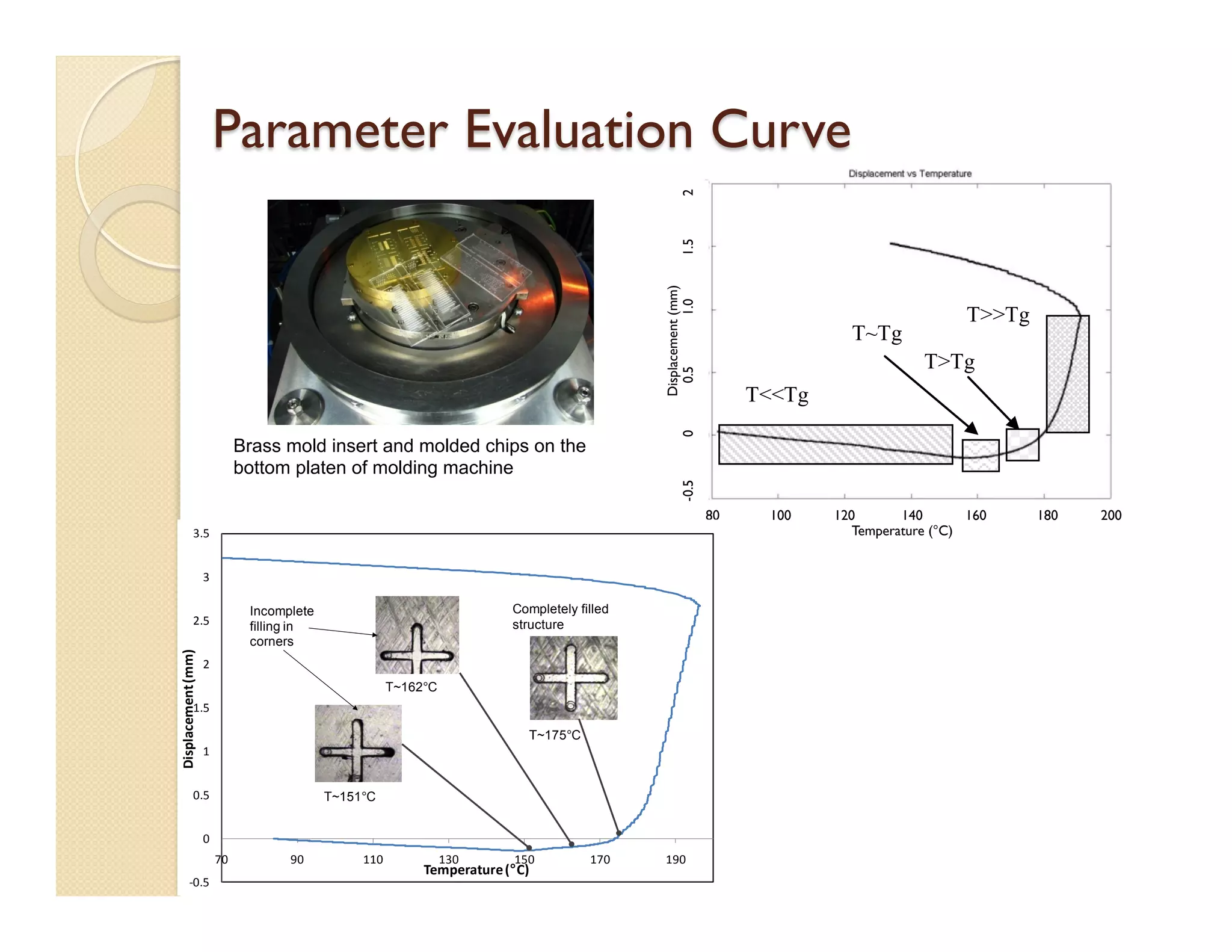
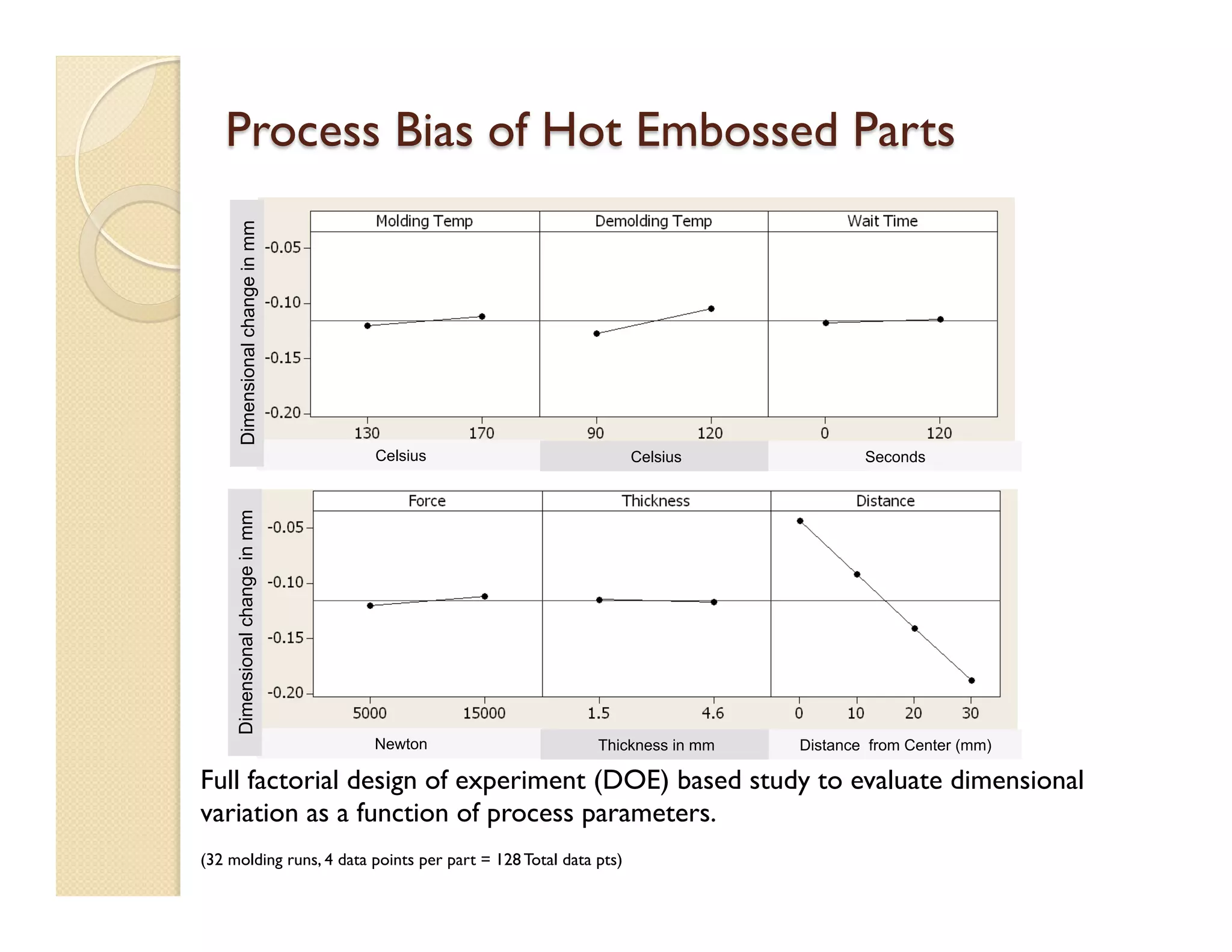
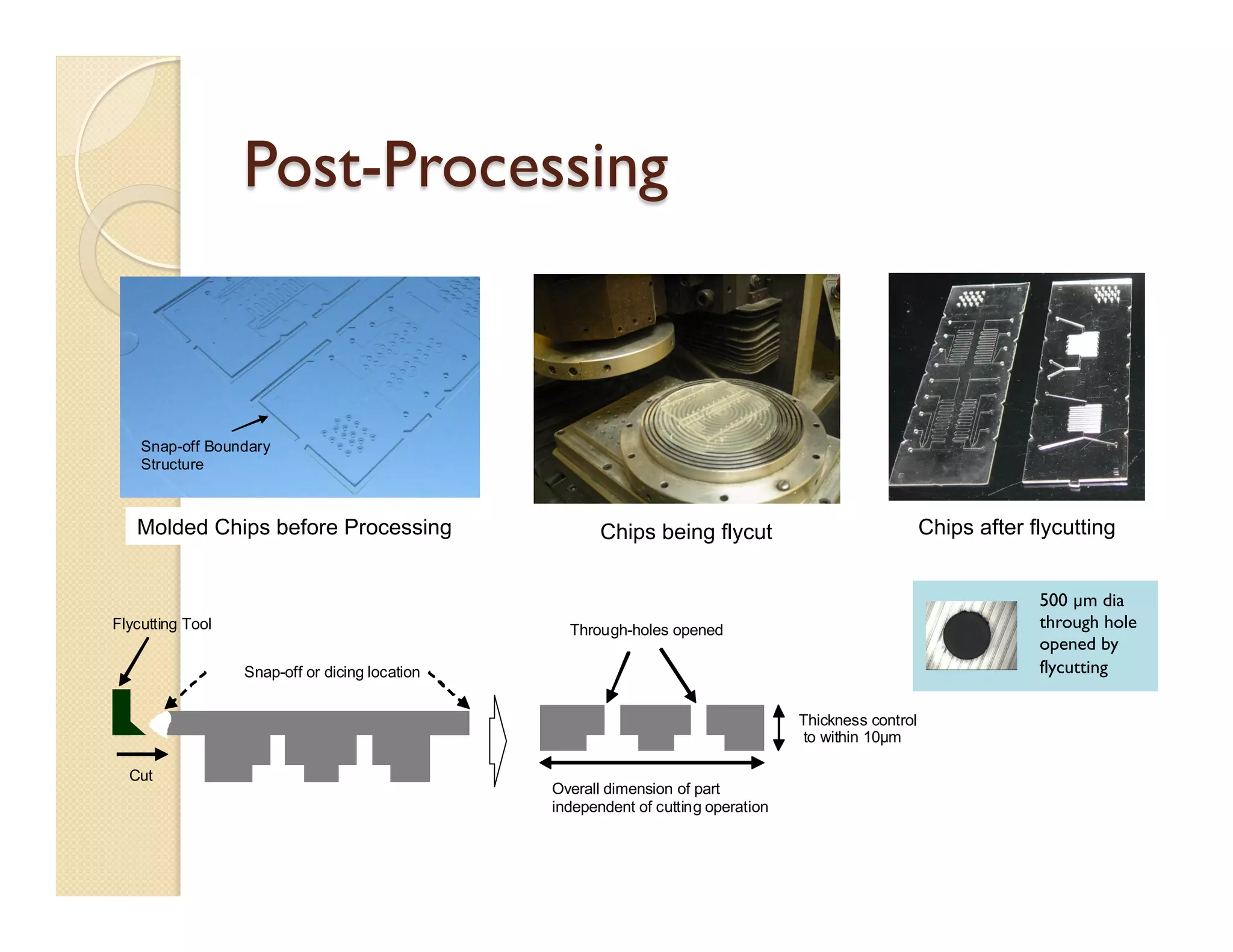
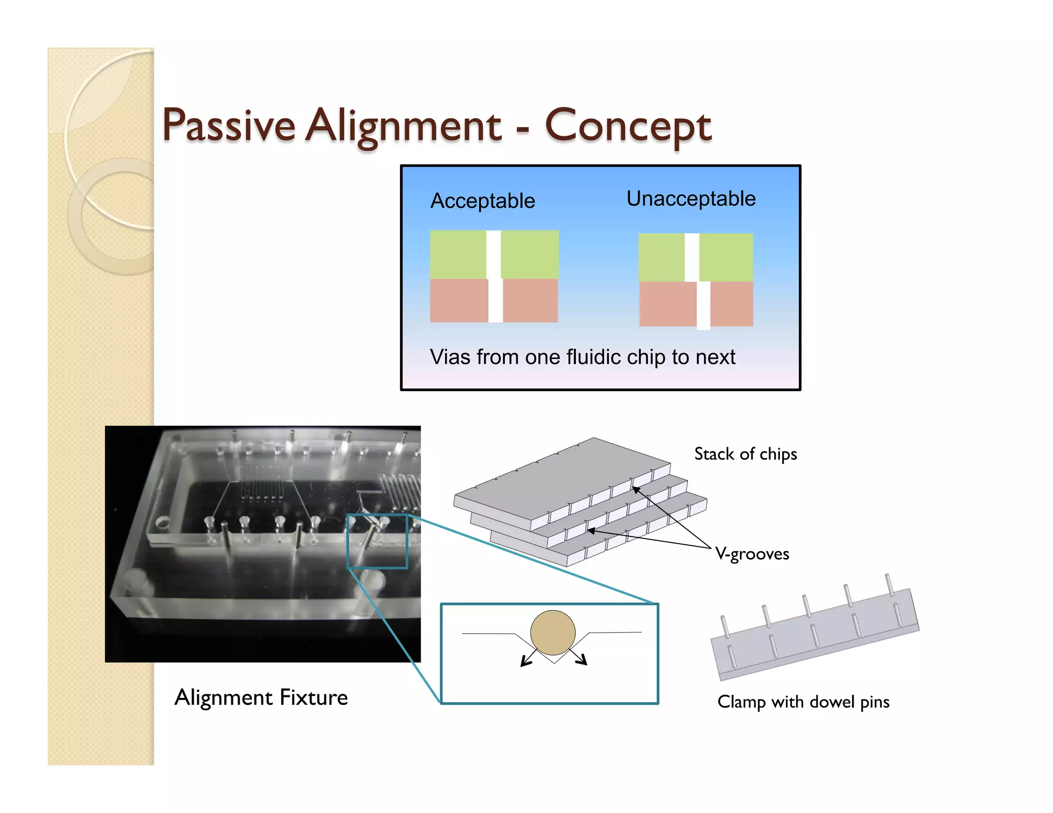
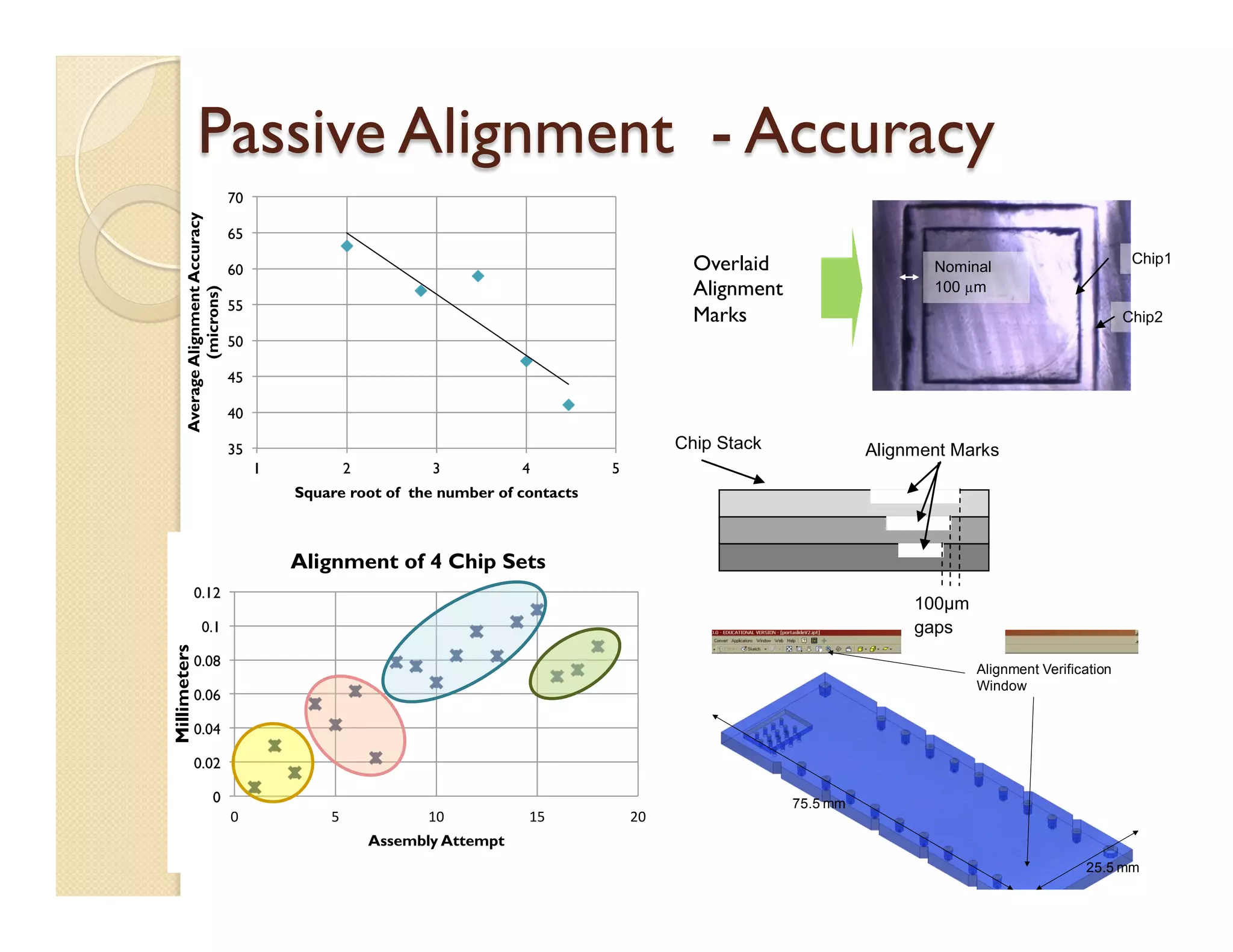
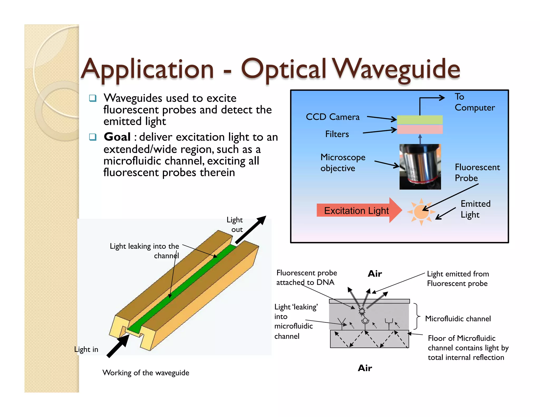
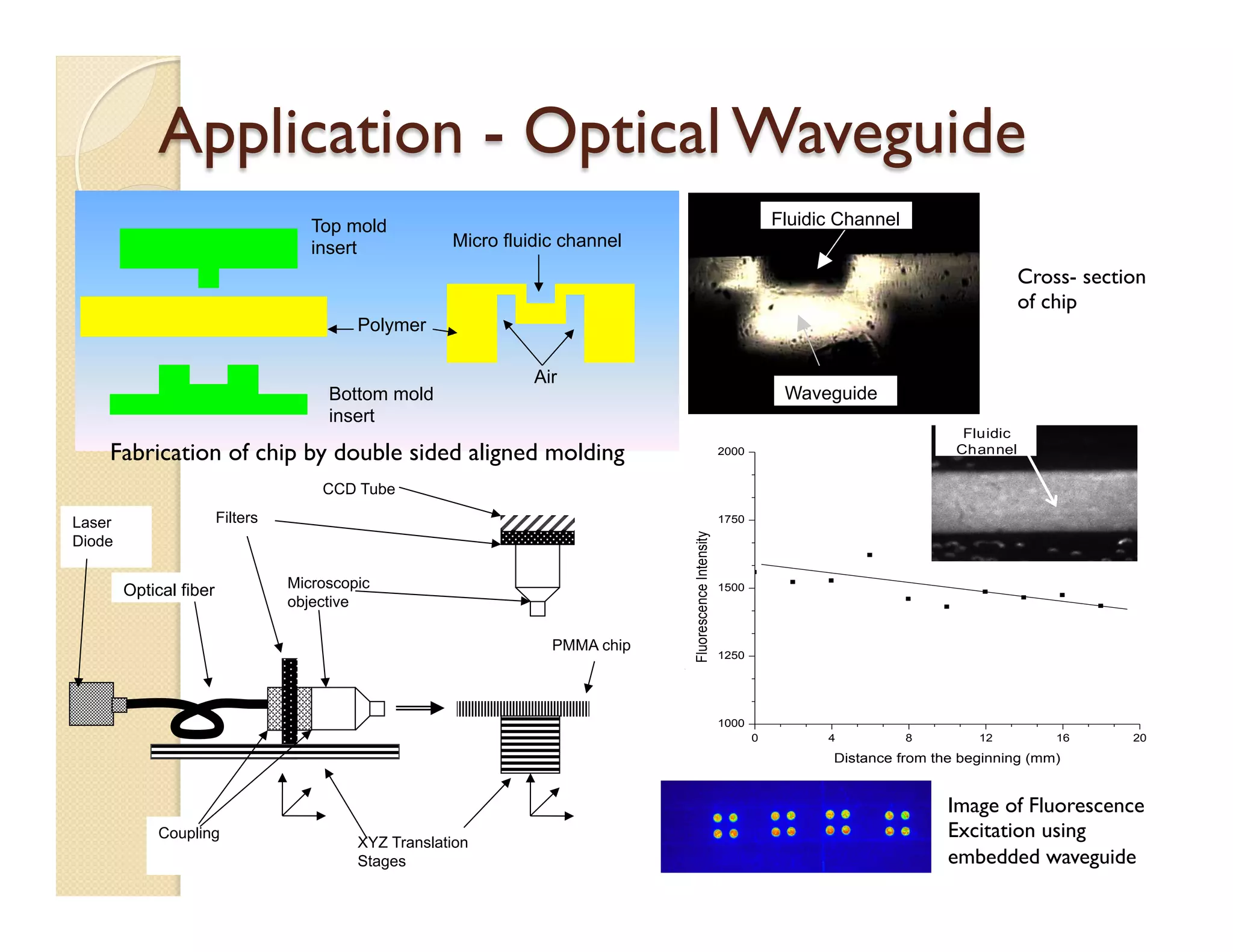
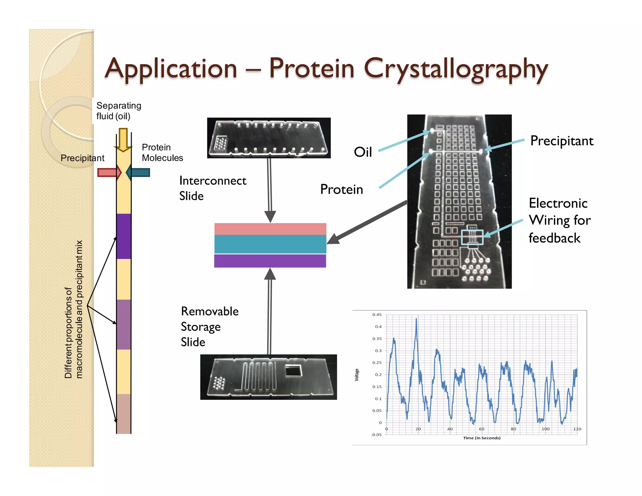
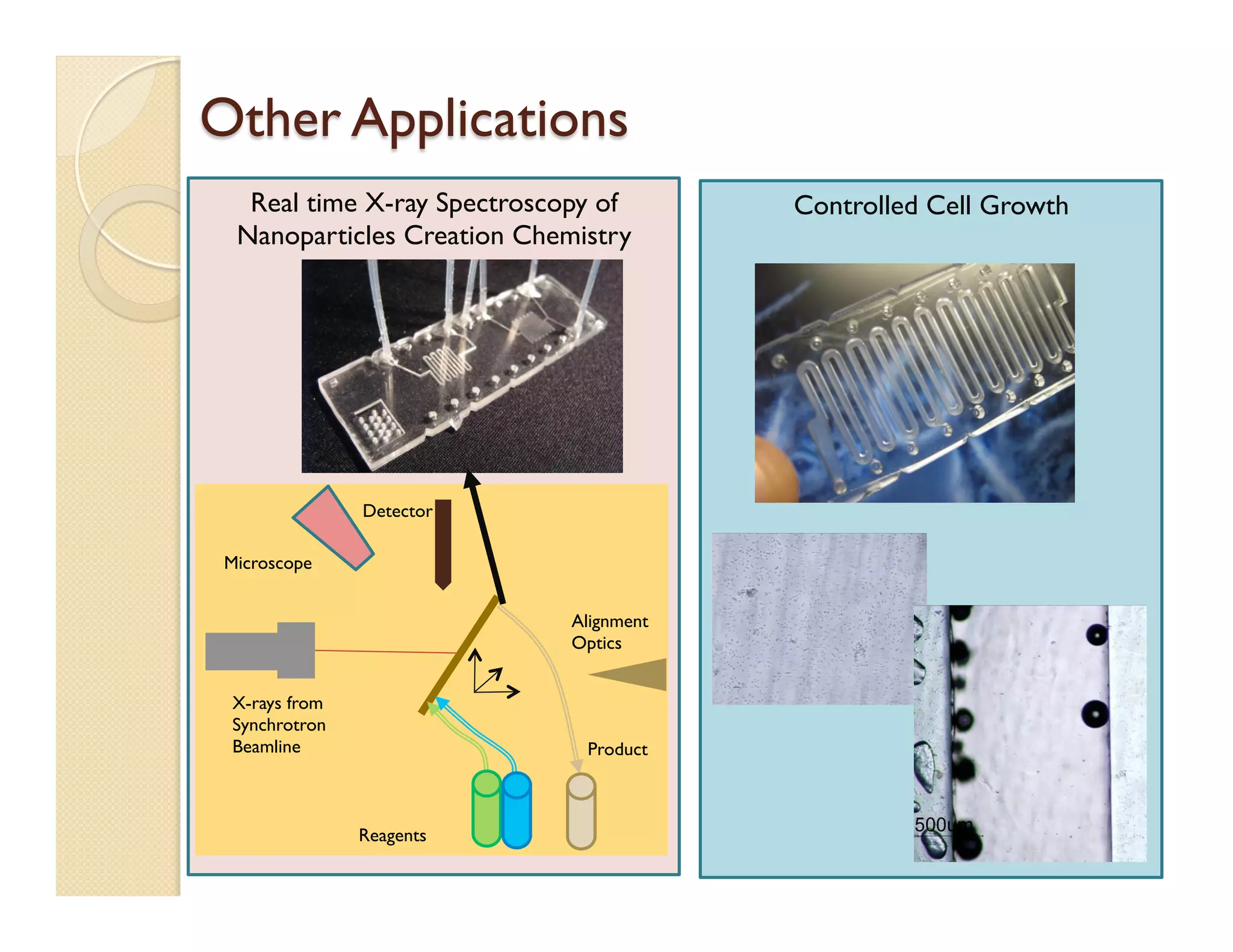
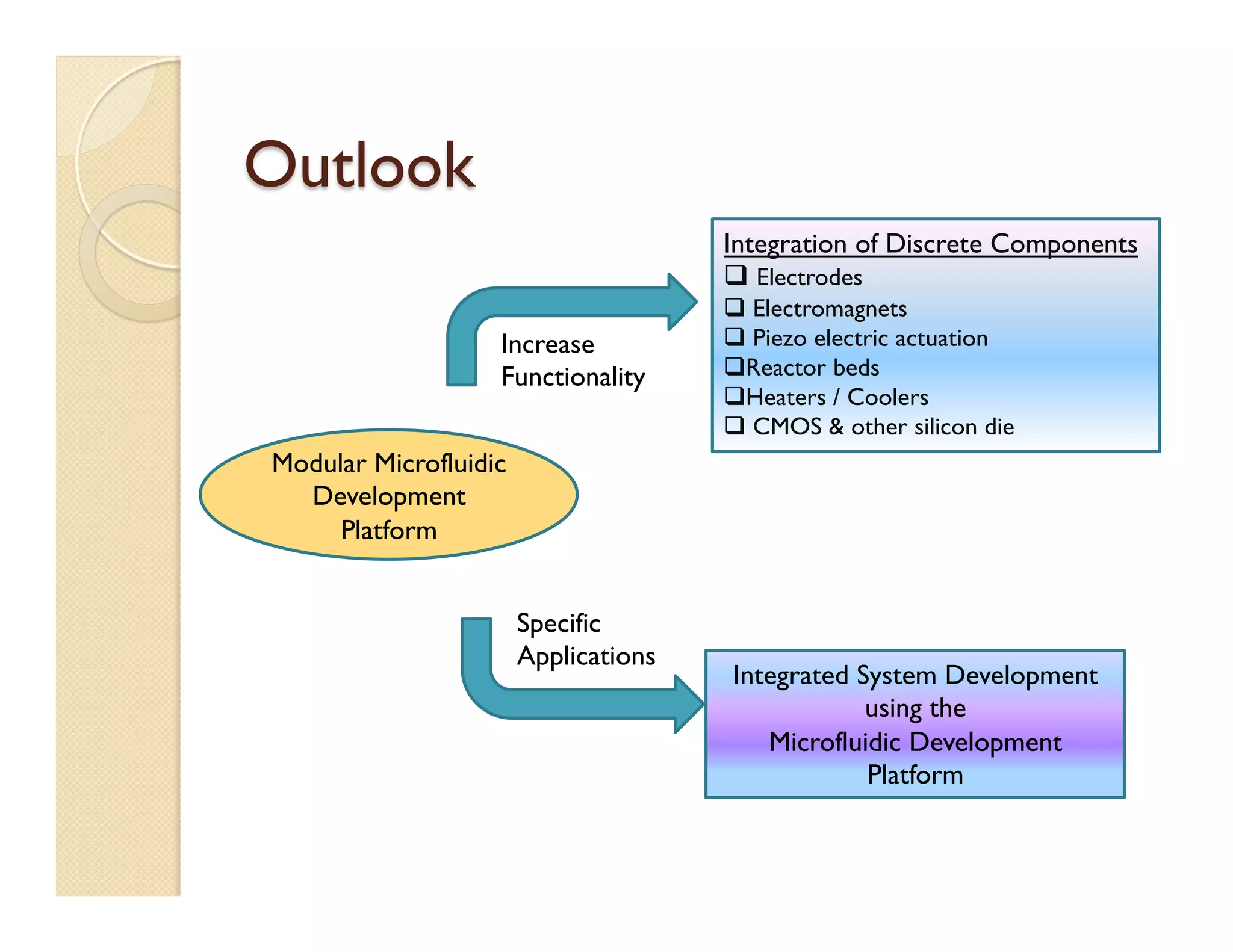
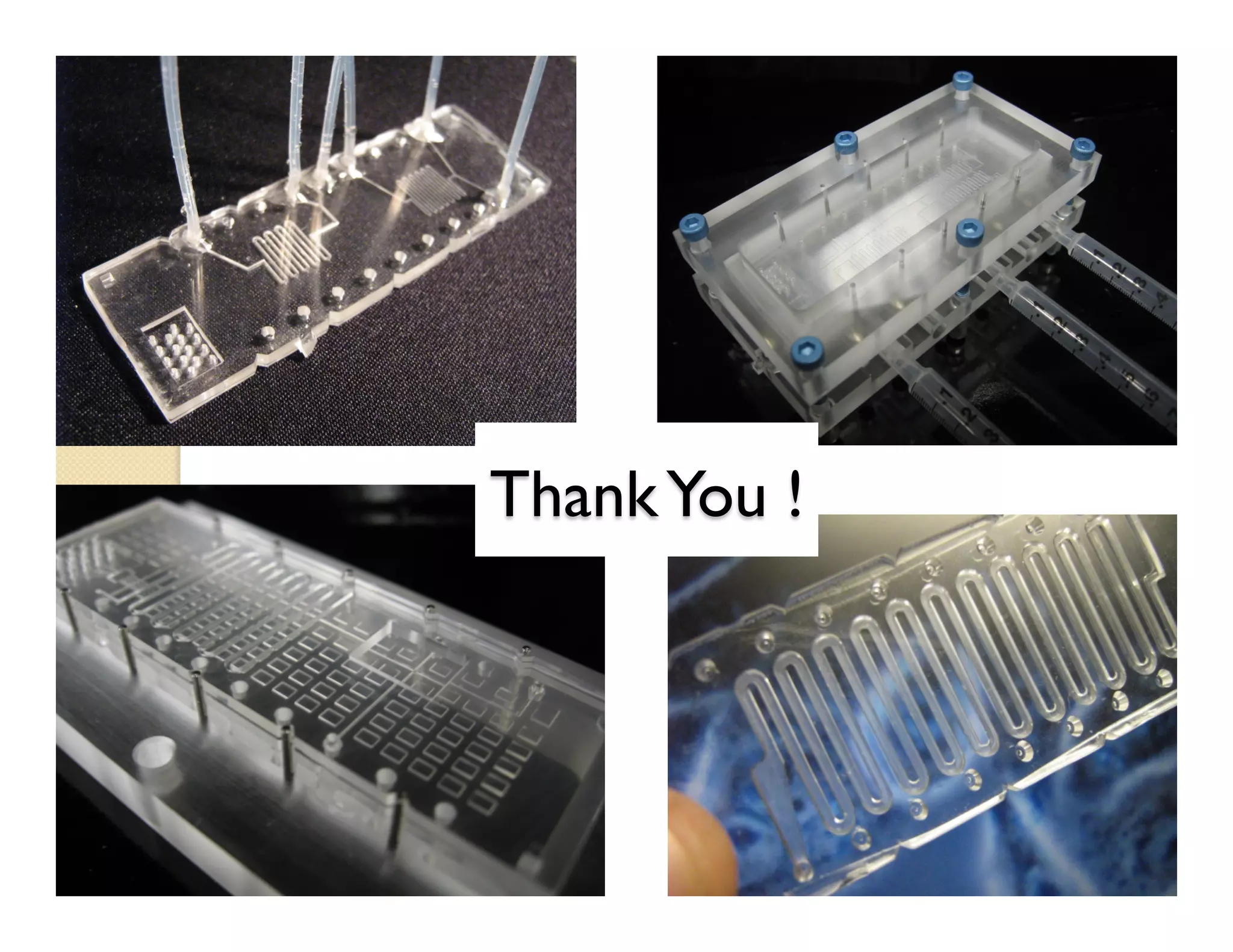

The document describes a modular polymeric development platform for microfluidic applications. Key points: - The goal is to design, build, and test a general-purpose microfluidic development platform to enable transition from prototype to mass production. - The platform uses vertically stacked, modular microfluidic chips that can be easily assembled and interfaced with external components through fluidic and electrical interconnects. - Fabrication involves molding polymer chips using hot embossing, then post-processing like flycutting. Various applications are demonstrated including surface chemistry, optical waveguides, and protein crystallization. - The platform provides a standardized, low-cost and user-friendly system for developing and testing microfluid