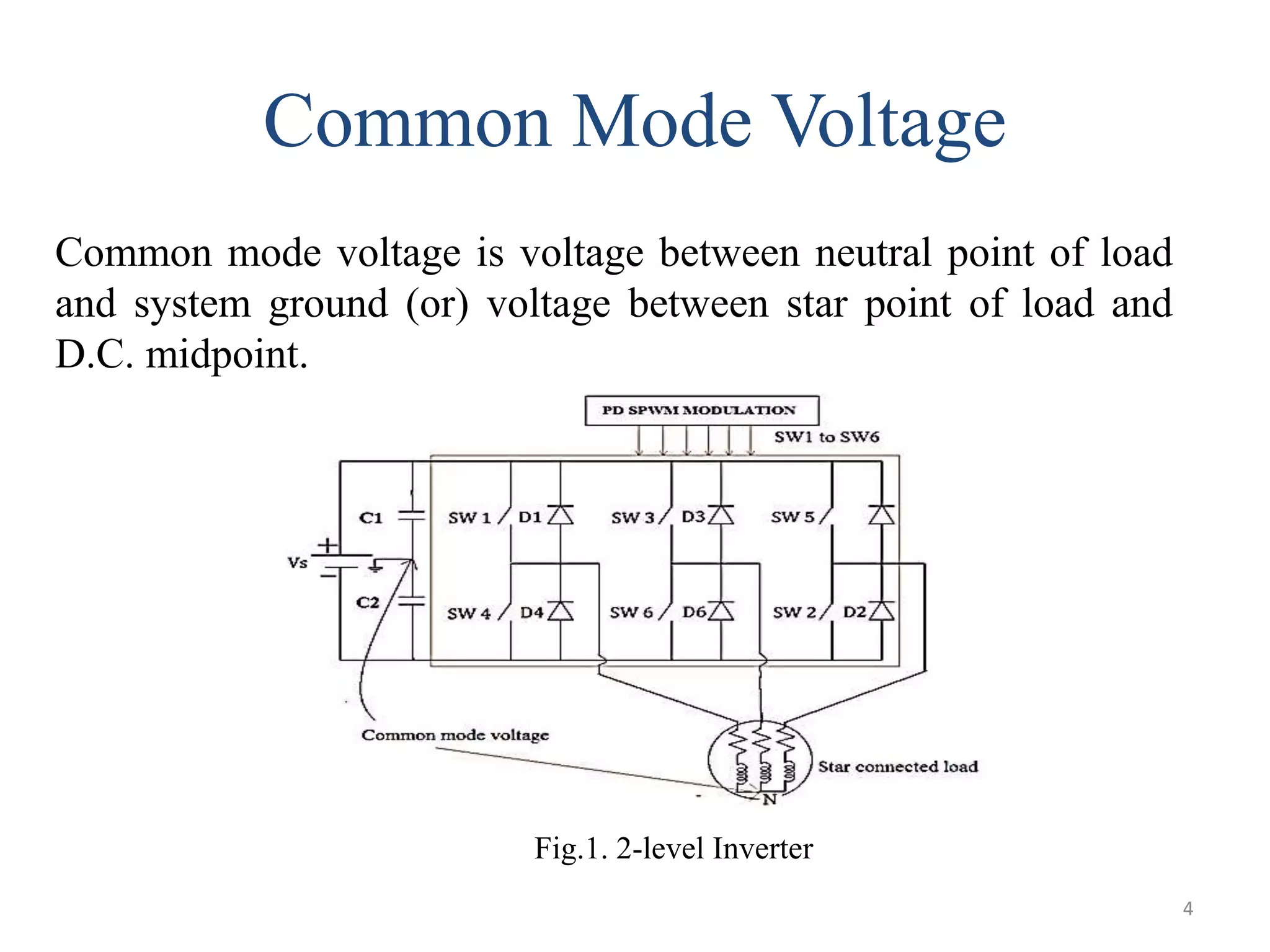
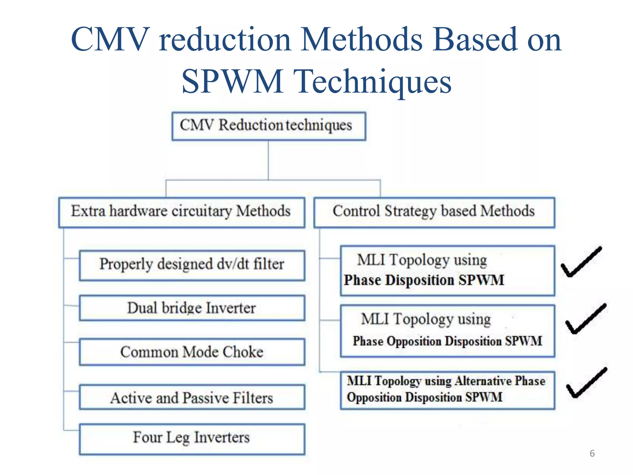
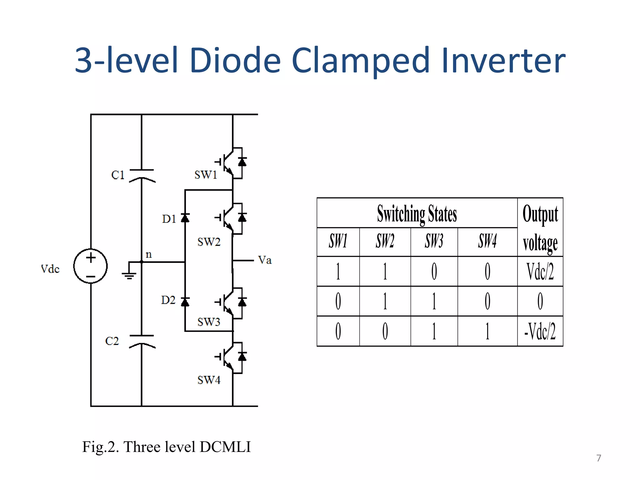
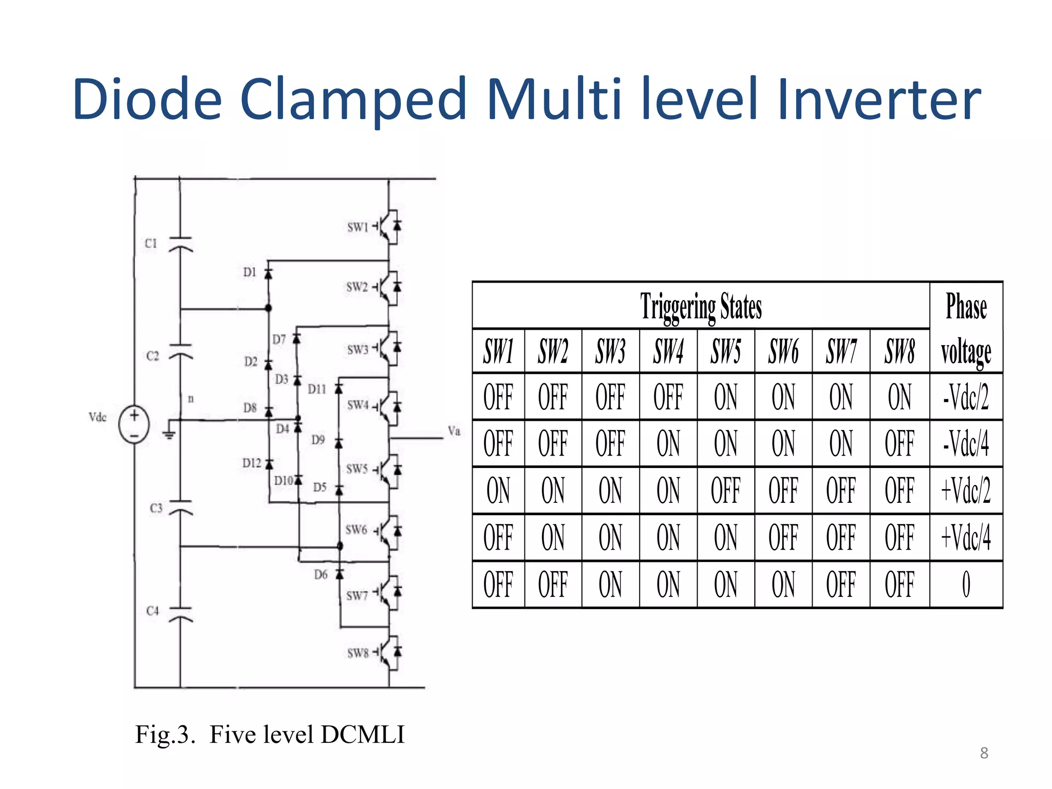
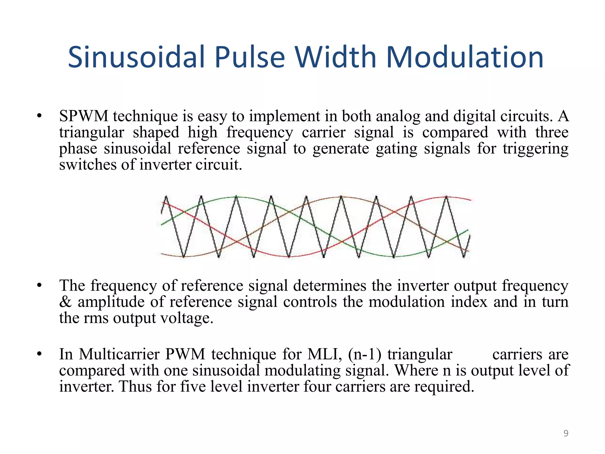
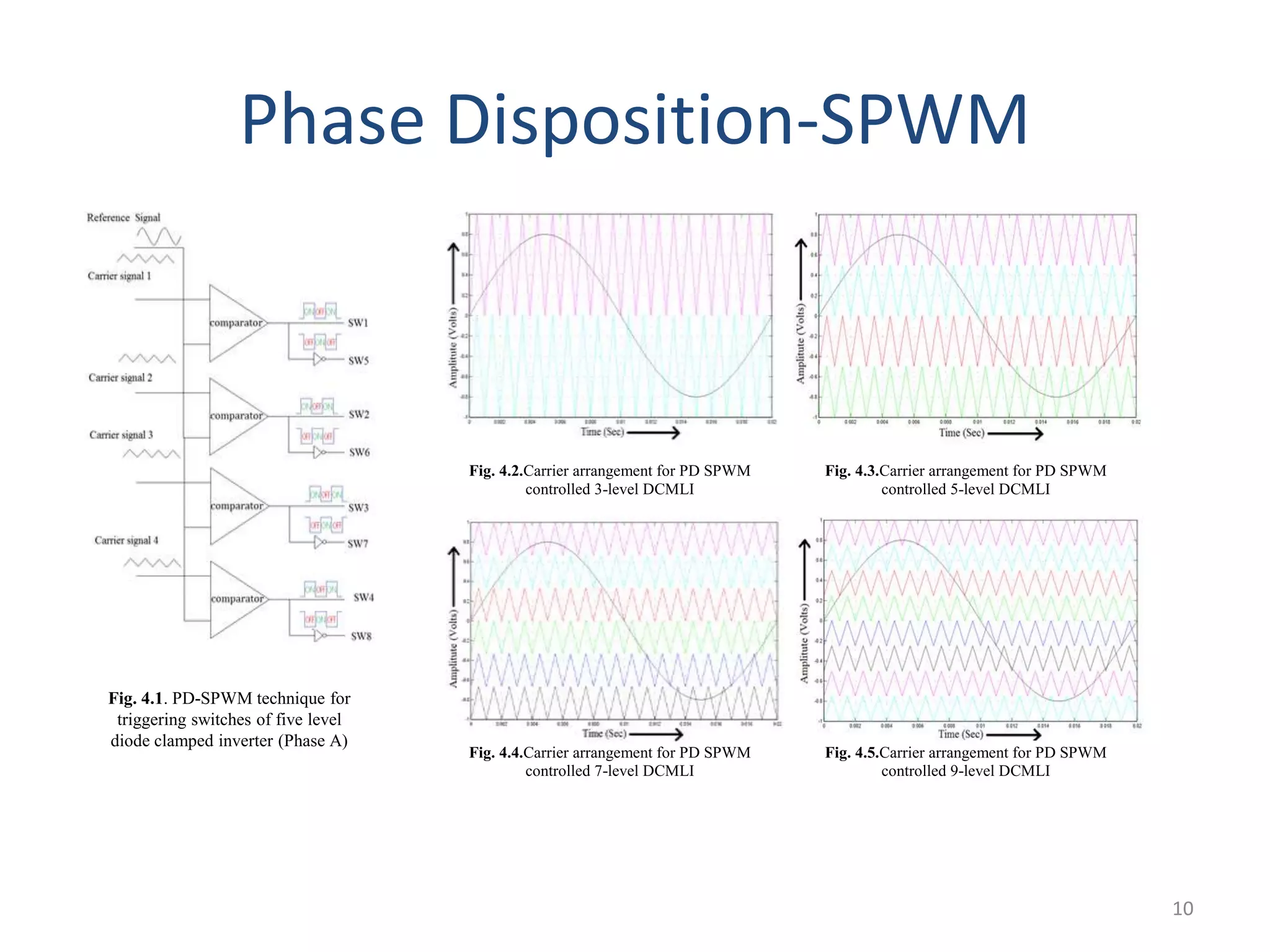
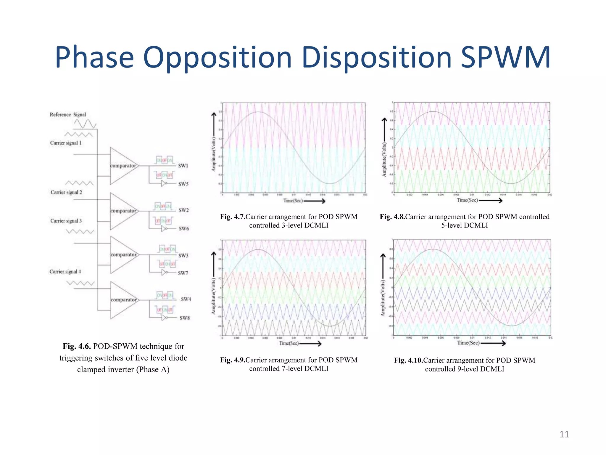
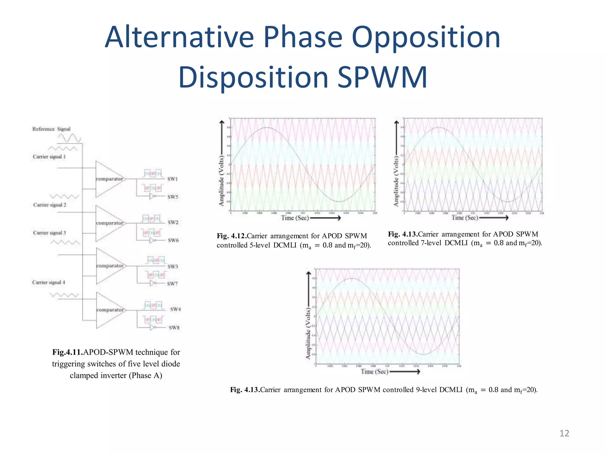
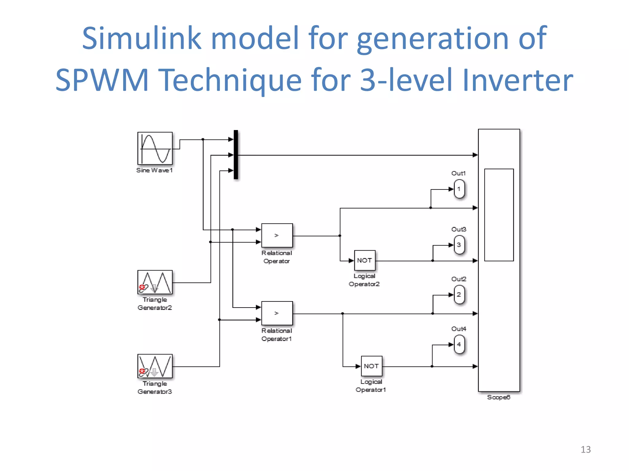
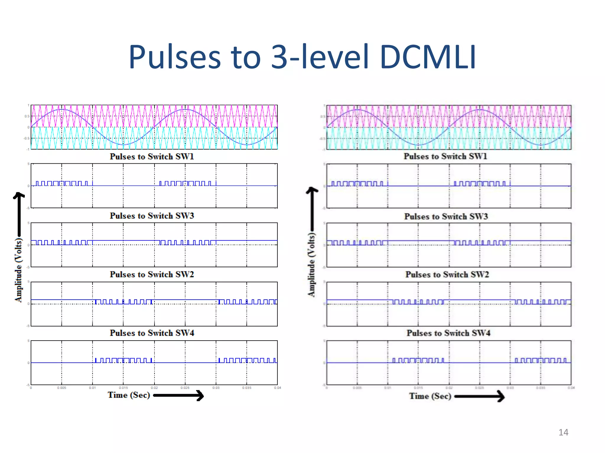
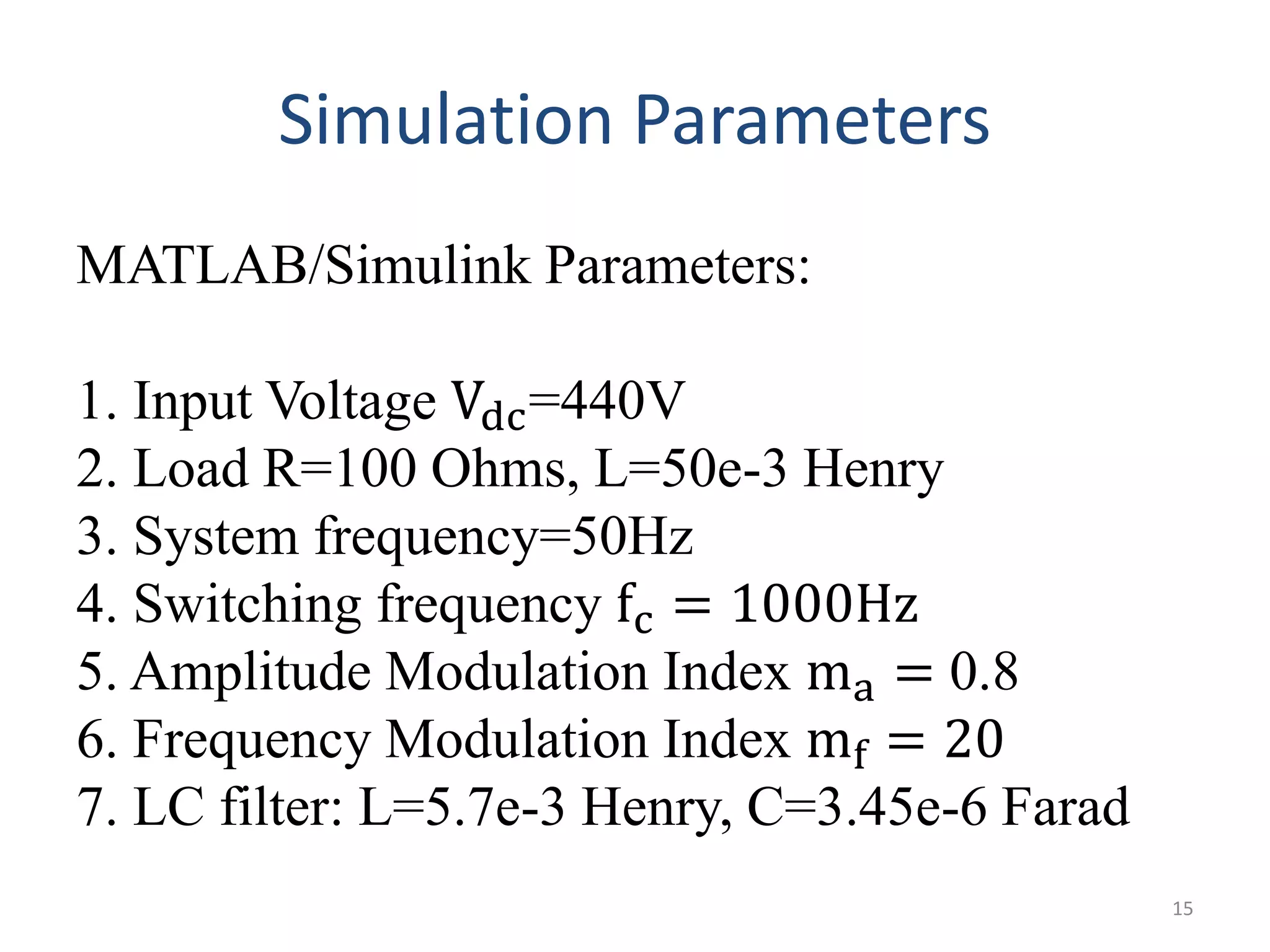
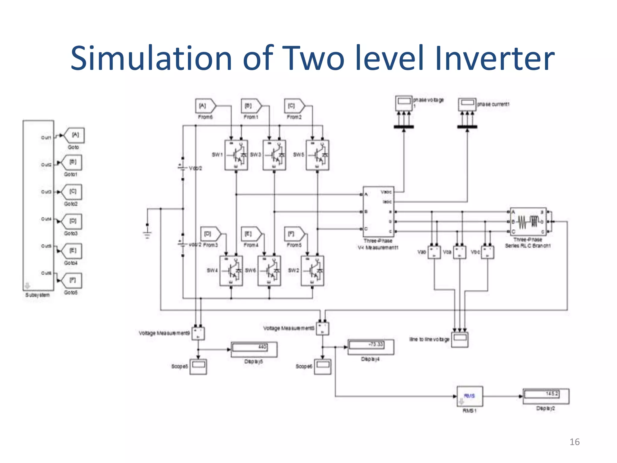
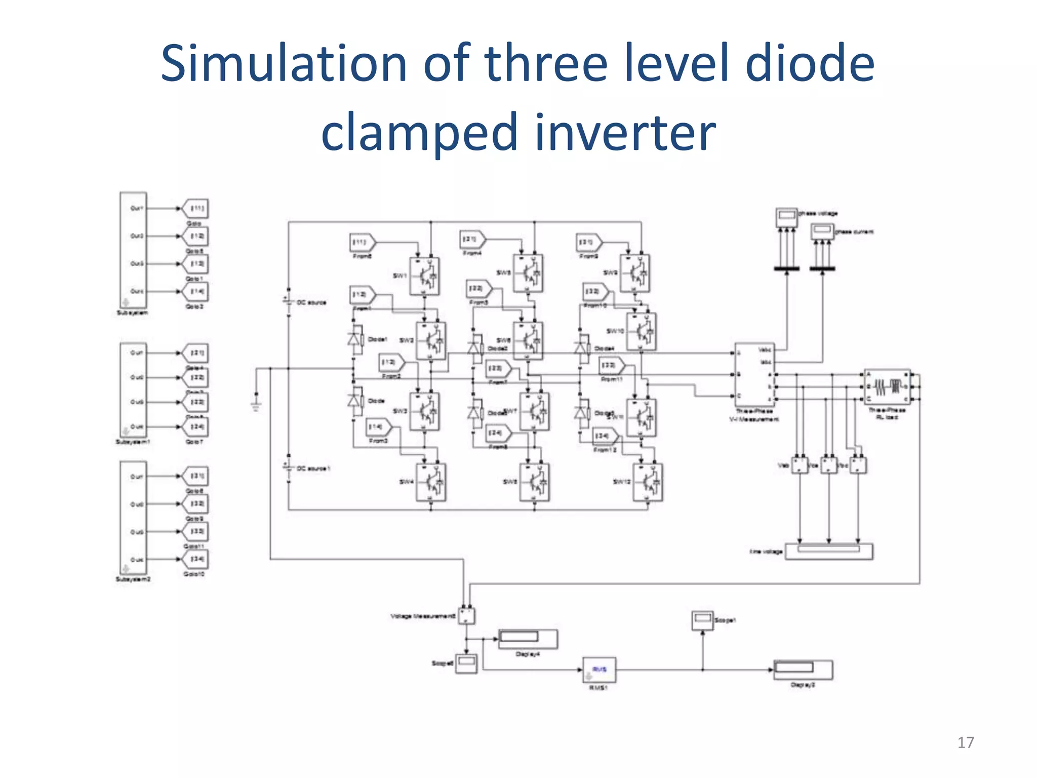
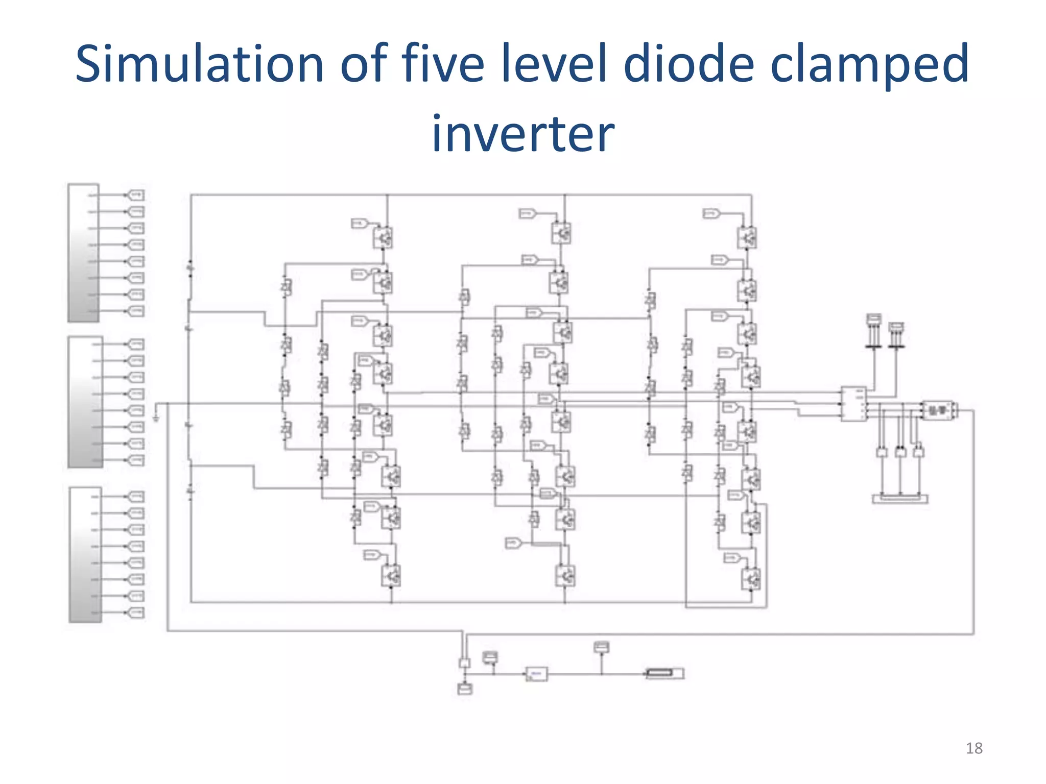
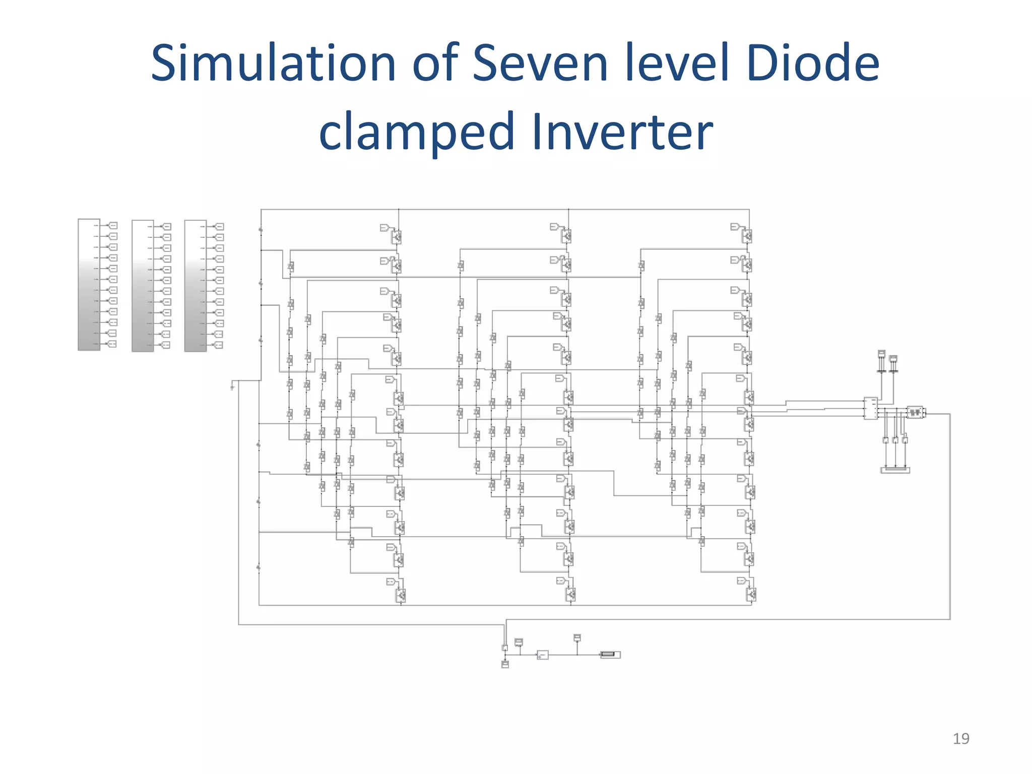
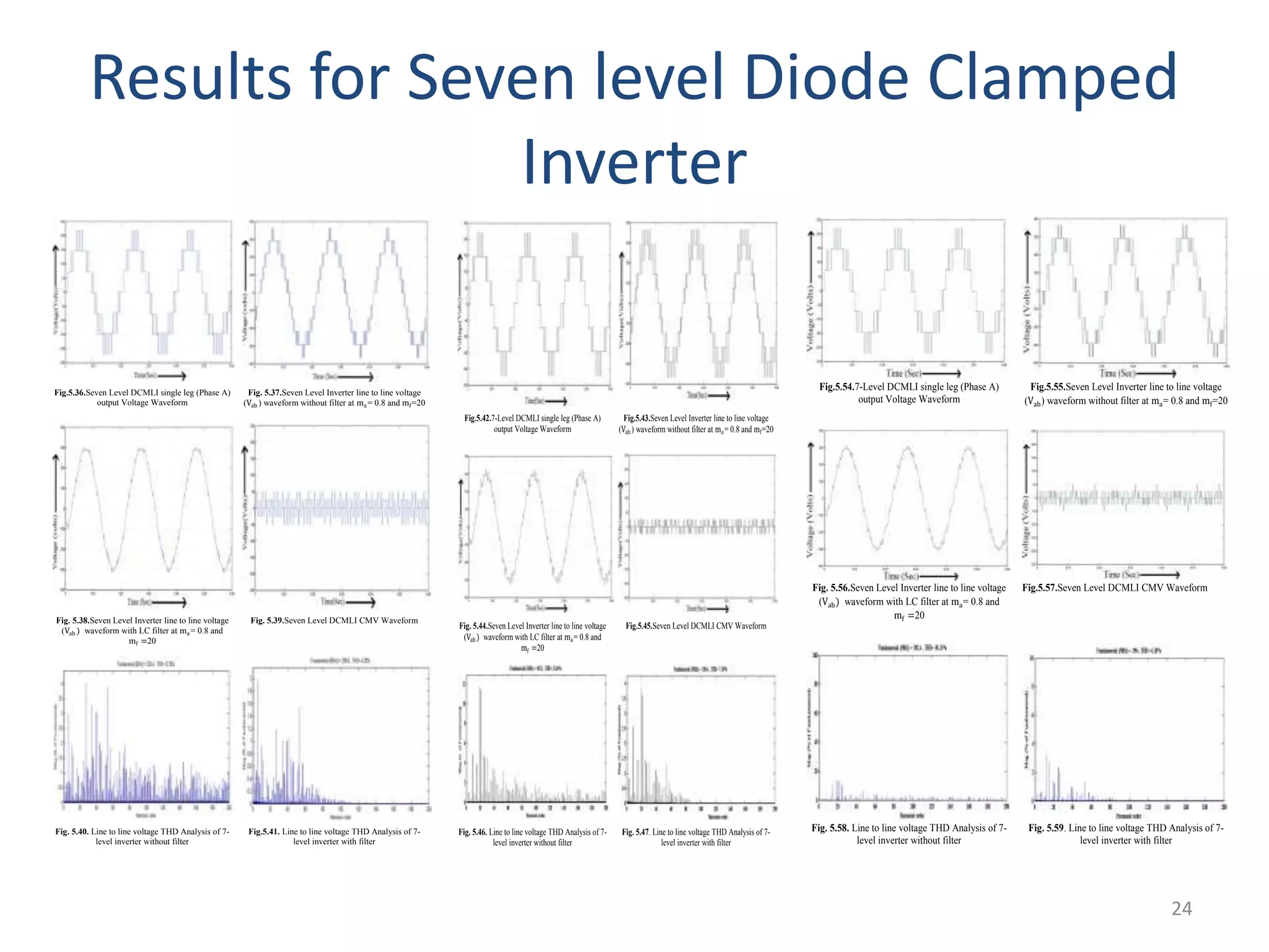
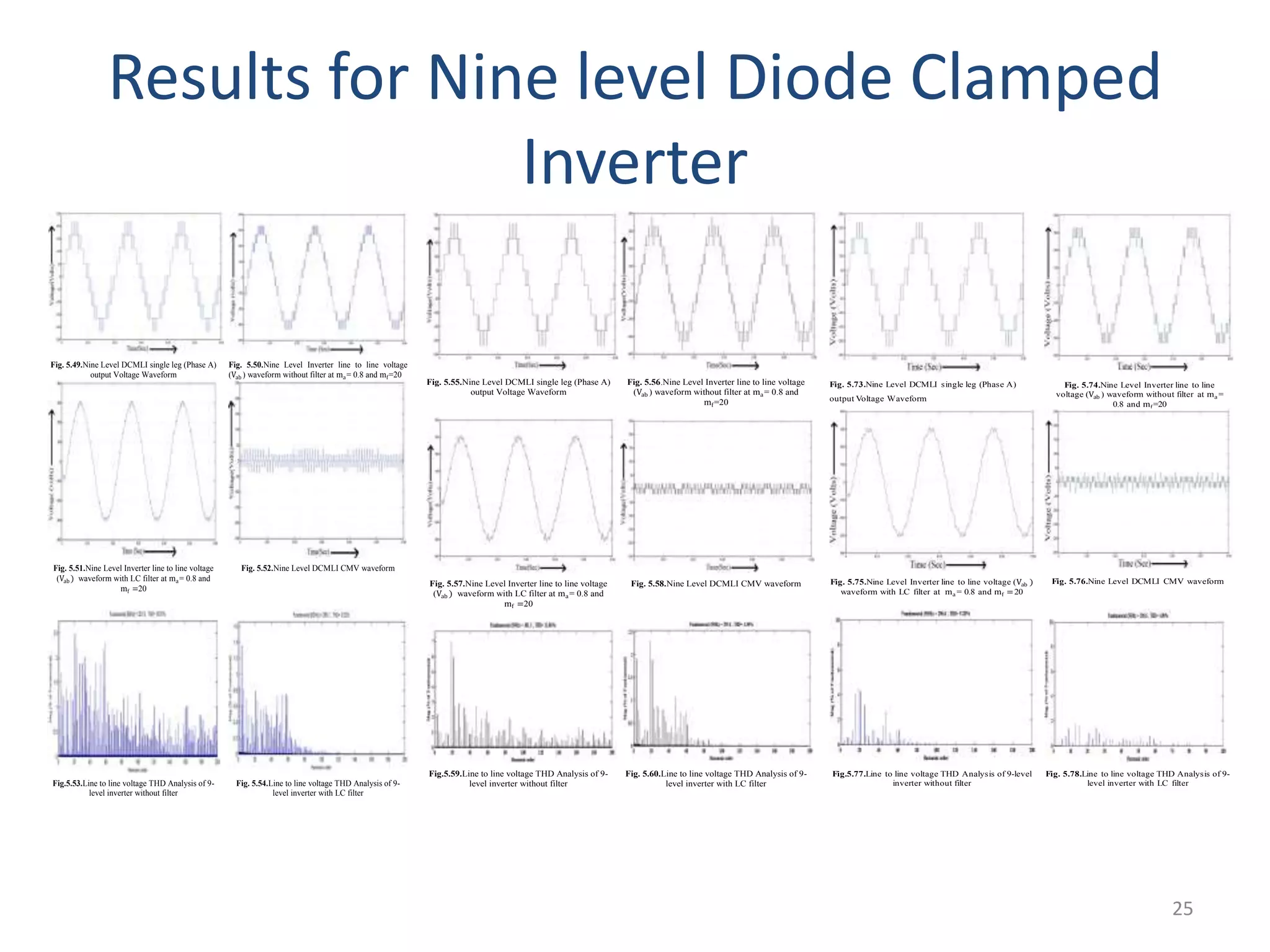
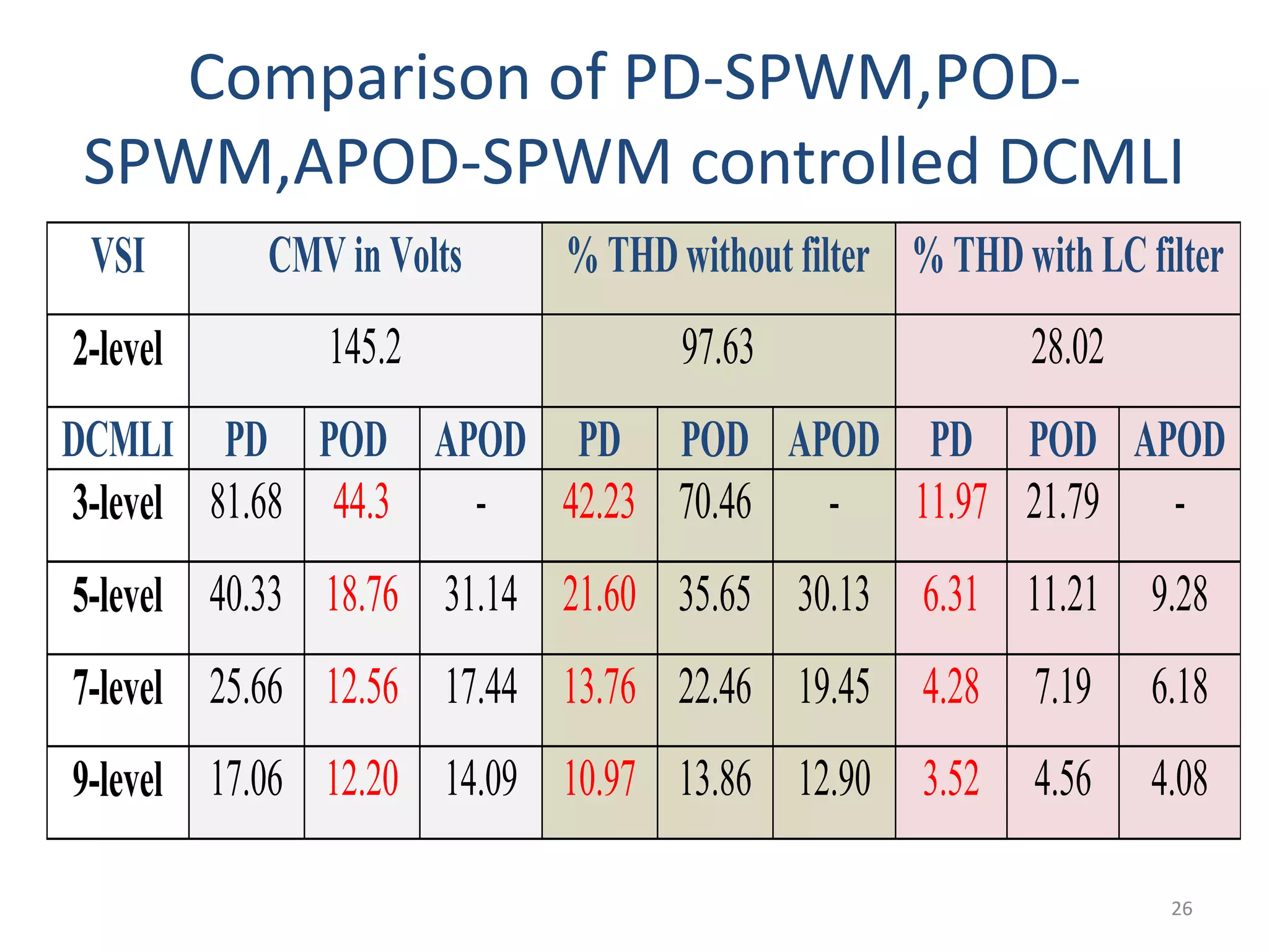
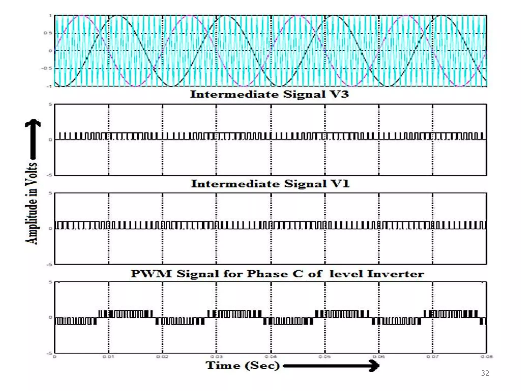
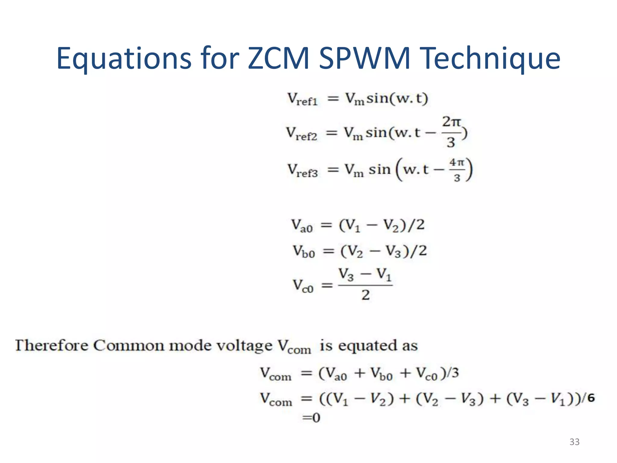
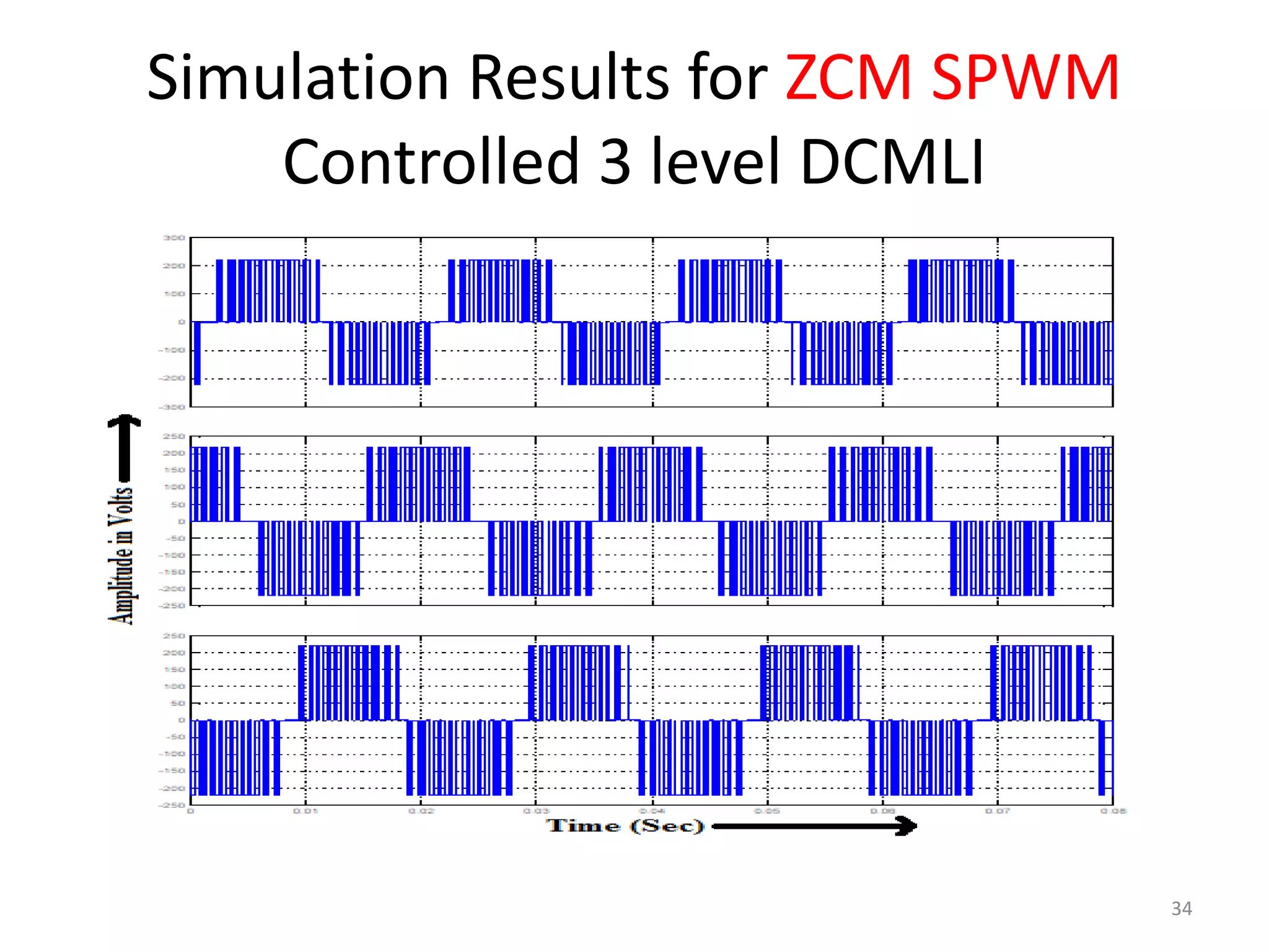
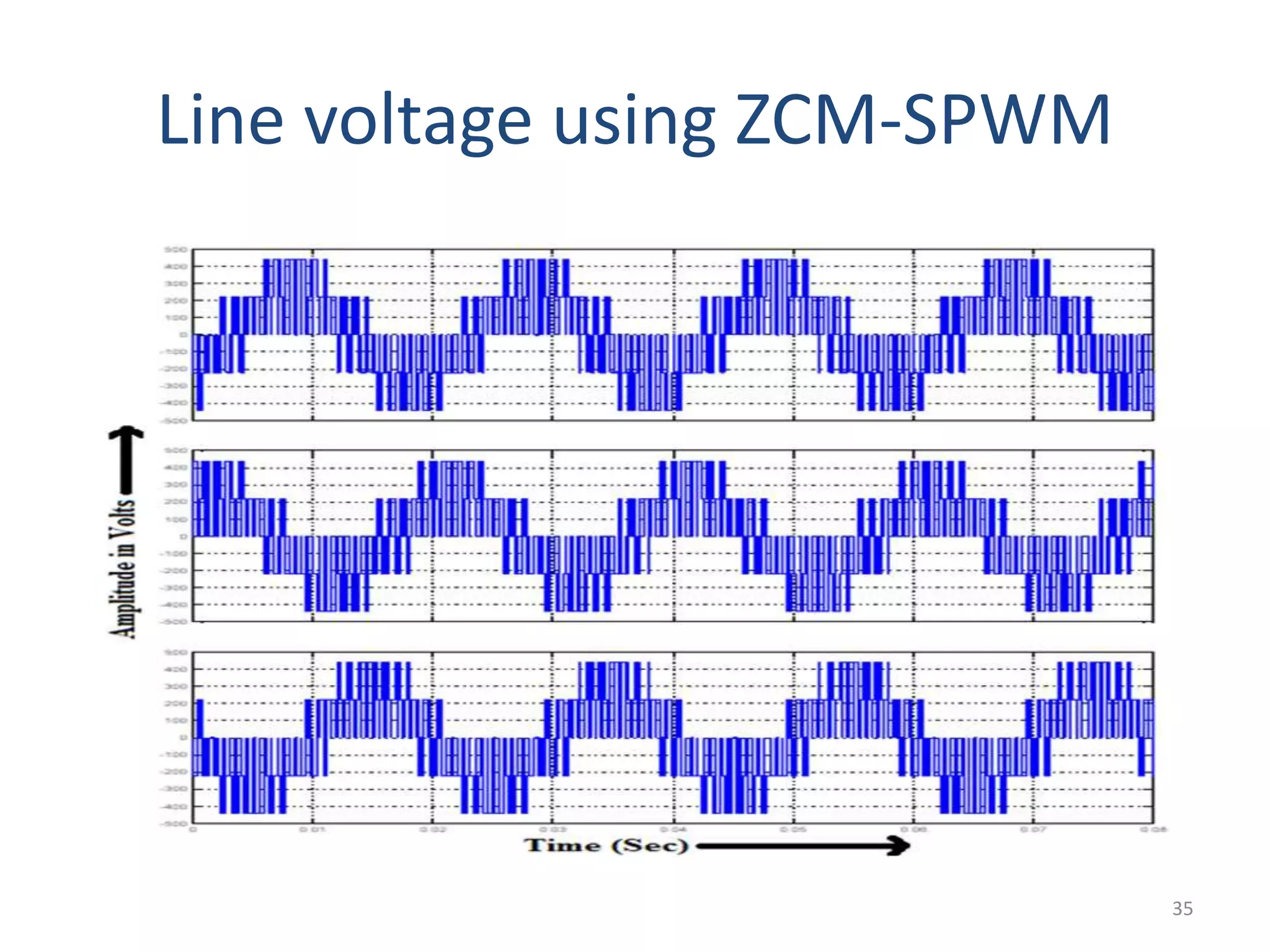
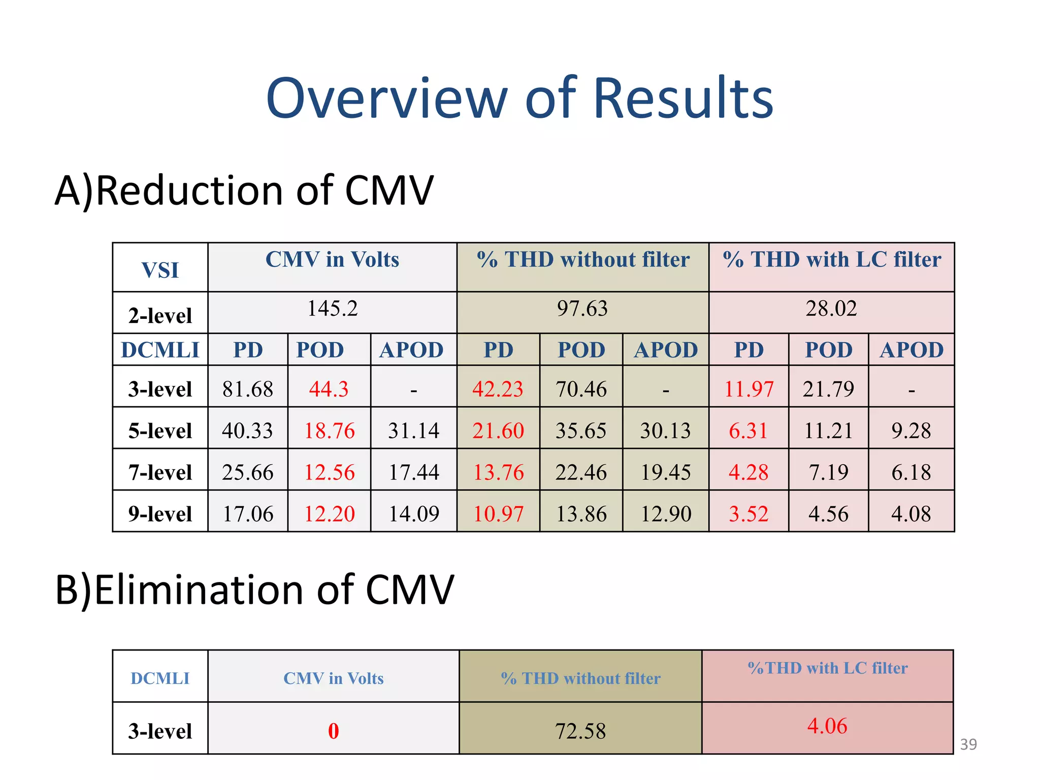
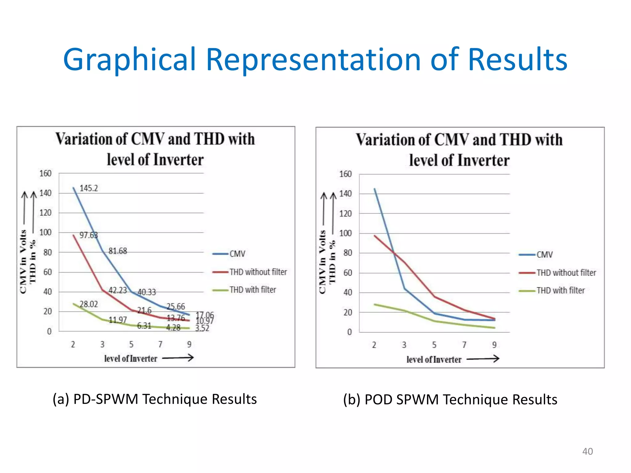
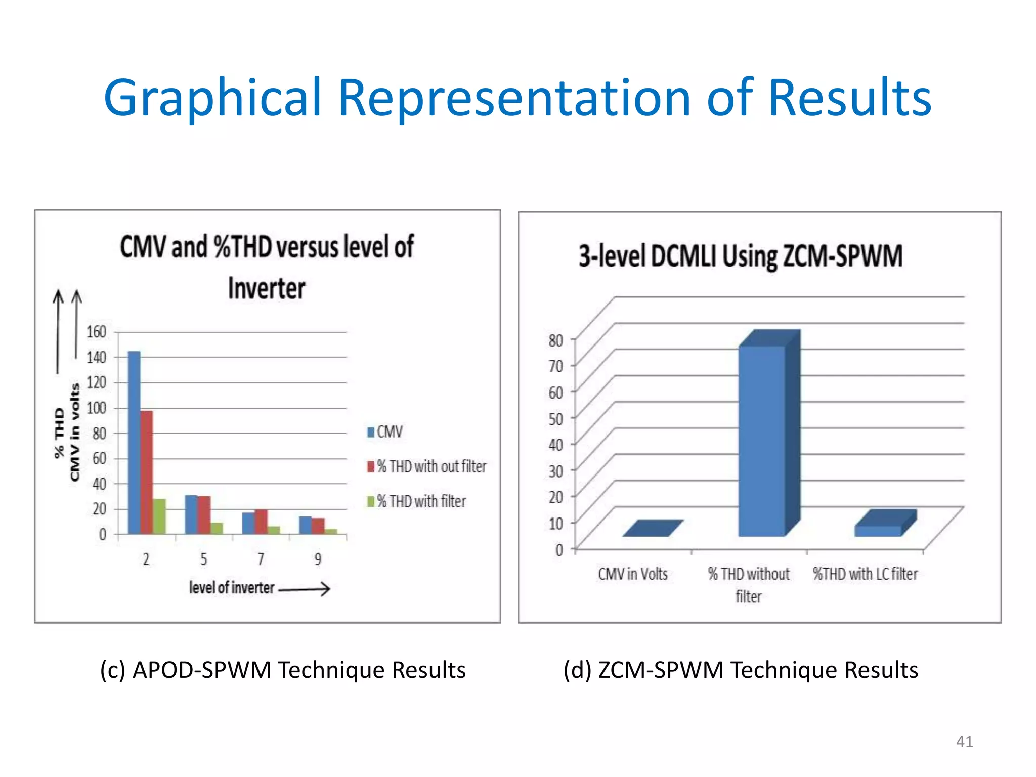
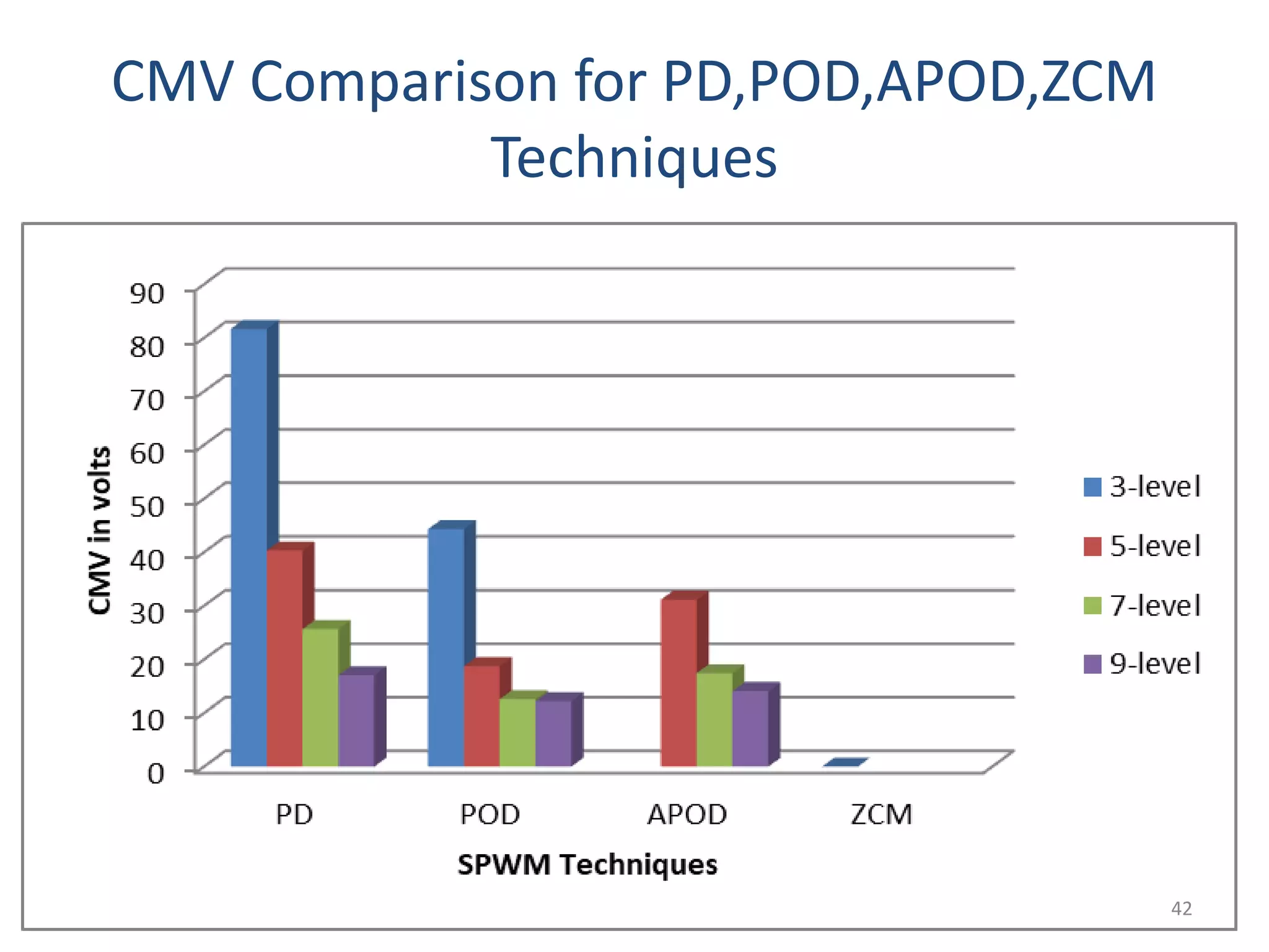
COMMON MODE VOLTAGE REDUCTION IN DIODE CLAMPED
MLI USING SPWM TECHNIQUES
By
MohdEsa
1604-16-743-002
Power ElectronicSystems
Under the guidance
of
Mr.J.E.Muralidhar
AssociateProfessor
ElectricalEngineeringDepartment
MuffakhamJah Collegeof Engineering and Technology
2018
Contents
 Objective
 Common mode voltage
 Effects of Common mode voltage
 Methods to reduce Common mode voltage
 Diode clamped MLI
 SPWM Techniques
 Simulation Models of 3,5,7,9 level DCMLI
 Simulation results
 Comparison of results through graphical representation
 Conclusion
 References
 Papers Published
2
Objective
• The objective of this project is to reduce the Common Mode
Voltage (CMV) in Diode Clamped Multilevel Inverter
(DCMLI). Three phase star connected RL load is connected to
DCMLI.
• In this project,PD-SPWM,POD SPWM,APOD SPWM
technique is used to reduce common mode voltage
• The simulation of circuit is carried out by using
MATLAB/Simulink.
3
Common Mode Voltage
Common mode voltage is voltage between neutral point of load
and system ground (or) voltage between star point of load and
D.C. midpoint.
Fig.1. 2-level Inverter
4
Effects of CMV
a) Regardless of number of legs & levels, high amplitude &
high frequency CMV exists always in pulse width
modulated inverters because of its switching operation
which causes common mode current (CMC) through
parasitic capacitor components between inverter, loads &
ground respectively. This CMC cause’s mal operation of
inverter control system as it is a source of electromagnetic
interference noise [1].
b) Shaft voltages on the rotor are caused by pulse width
modulated inverters because of CMV.Premature failure of
IM bearings is caused when this shaft voltage exceeds the
voltage limit of lubricant in the bearings.CMV is necessary
to reduce by choosing specific reduction technique [2].
5
CMV reduction Methods Based on
SPWM Techniques
Fig. 2.CMV reduction techniques
6
3-level Diode Clamped Inverter
SwitchingStates Output
voltageSW1 SW2 SW3 SW4
1 1 0 0 Vdc/2
0 1 1 0 0
0 0 1 1 -Vdc/2
Fig.2. Three level DCMLI
7
Diode Clamped Multi level Inverter
Fig.3. Five level DCMLI
TriggeringStates Phase
voltageSW1 SW2 SW3 SW4 SW5 SW6 SW7 SW8
OFF OFF OFF OFF ON ON ON ON -Vdc/2
OFF OFF OFF ON ON ON ON OFF -Vdc/4
ON ON ON ON OFF OFF OFF OFF +Vdc/2
OFF ON ON ON ON OFF OFF OFF +Vdc/4
OFF OFF ON ON ON ON OFF OFF 0
8
Sinusoidal Pulse Width Modulation
• SPWM technique is easy to implement in both analog and digital circuits. A
triangular shaped high frequency carrier signal is compared with three
phase sinusoidal reference signal to generate gating signals for triggering
switches of inverter circuit.
• The frequency of reference signal determines the inverter output frequency
& amplitude of reference signal controls the modulation index and in turn
the rms output voltage.
• In Multicarrier PWM technique for MLI, (n-1) triangular carriers are
compared with one sinusoidal modulating signal. Where n is output level of
inverter. Thus for five level inverter four carriers are required.
9
Phase Disposition-SPWM
Fig. 4.2.Carrier arrangement for PD SPWM
controlled 3-level DCMLI
Fig. 4.3.Carrier arrangement for PD SPWM
controlled 5-level DCMLI
Fig. 4.4.Carrier arrangement for PD SPWM
controlled 7-level DCMLI
Fig. 4.5.Carrier arrangement for PD SPWM
controlled 9-level DCMLI
Fig. 4.1. PD-SPWM technique for
triggering switches of five level
diode clamped inverter (Phase A)
10
Phase Opposition Disposition SPWM
Fig. 4.7.Carrier arrangement for POD SPWM
controlled 3-level DCMLI
Fig. 4.8.Carrier arrangement for POD SPWM controlled
5-level DCMLI
Fig. 4.9.Carrier arrangement for POD SPWM
controlled 7-level DCMLI
Fig. 4.10.Carrier arrangement for POD SPWM
controlled 9-level DCMLI
Fig. 4.6. POD-SPWM technique for
triggering switches of five level diode
clamped inverter (Phase A)
11
Alternative Phase Opposition
Disposition SPWM
Fig. 4.12.Carrier arrangement for APOD SPWM
controlled 5-level DCMLI (ma = 0.8 and mf=20).
Fig. 4.13.Carrier arrangement for APOD SPWM
controlled 7-level DCMLI (ma = 0.8 and mf=20).
Fig. 4.13.Carrier arrangement for APOD SPWM controlled 9-level DCMLI (ma = 0.8 and mf=20).
Fig.4.11.APOD-SPWM technique for
triggering switches of five level diode
clamped inverter (Phase A)
12
Simulink model for generation of
SPWM Technique for 3-level Inverter
13
Pulses to 3-level DCMLI
14
Simulation Parameters
MATLAB/Simulink Parameters:
1. Input Voltage Vdc=440V
2. Load R=100 Ohms, L=50e-3 Henry
3. System frequency=50Hz
4. Switching frequency fc = 1000Hz
5. Amplitude Modulation Index ma = 0.8
6. Frequency Modulation Index mf = 20
7. LC filter: L=5.7e-3 Henry, C=3.45e-6 Farad
15
Simulation of Two level Inverter
16
Simulation of three level diode
clamped inverter
17
Simulation of five level diode clamped
inverter
18
Simulation of Seven level Diode
clamped Inverter
19
Simulation of Nine level Diode
clamped Inverter
20
Results for 2 level Inverter
21
Results for
3 level Diode clamped Inverter
Fig. 5.10.Three- Level DCMLI single leg (Phase
A) output Voltage Waveform
Fig. 5.11.Three Level Inverter line to line voltage
(Vab ) waveform without filter at ma = 0.8 and mf=20
Fig. 5.12.Three Level Inverter line to line voltage
(Vab ) waveform with LC filter at ma = 0.8 and
mf =20
Fig. 5.13.Three Level DCMLI CMV Waveform
Fig. 5.14. Line to line voltage THD Analysis of 3-
level inverter without filter
Fig. 5.15. Line to line voltage THD Analysis of 3-
level inverter with filter
Fig. 5.16.Three Level DCMLI single leg (Phase
A) output Voltage Waveform
Fig. 5.17.Three Level Inverter line to line voltage
(Vab ) waveform without filter at ma= 0.8 and mf=20
Fig. 5.18.Three Level Inverter line to line voltage
(Vab ) waveform with LC filter at ma= 0.8 and
mf =20
Fig. 5.19.Three Level DCMLI CMV Waveform
Fig. 5.20. Line to line voltage THD Analysis of 3-
level inverter without filter
Fig. 5.21. Line to line voltage THD Analysis of 3-
level inverter with filter
22
Results for 5 level Diode clamped
Inverter
Fig. 5.23.Five Level DCMLI single leg (Phase A)
output Voltage Waveform
Fig. 5.24.Five Level Inverter line to line voltage
(Vab ) waveform without filter at ma= 0.8 and mf=20
Fig. 5.25.Five Level Inverter line to line voltage
(Vab ) waveform with LC filter at ma= 0.8 and
mf =20
Fig. 5.26.Five Level DCMLI CMV Waveform
Fig.5.27. Line to line voltage THD Analysis of 5-
level inverter without filter
Fig. 5.28. Line to line voltage THD Analysis of 5-
level inverter with filter
Fig. 5.29.Five Level DCMLI single leg (Phase A)
output Voltage Waveform
Fig. 5.30.Five Level Inverter line to line voltage
(Vab ) waveform without filter at ma= 0.8 and mf=20
Fig. 5.31.Five Level Inverter line to line voltage
(Vab ) waveform with LC filter at ma= 0.8 and
mf =20
Fig. 5.32.Five Level DCMLI CMV Waveform
Fig. 5.33. Line to line voltage THD Analysis of 5-
level inverter without filter
Fig. 5.34. Line to line voltage THD Analysis of 5-
level inverter with filter
Fig. 5.35.Five Level DCMLI single leg (Phase A)
output Voltage Waveform
Fig. 5.36.Five Level Inverter line to line voltage
(Vab) waveform without filter at ma= 0.8 and mf=20
Fig. 5.37.Five Level Inverter line to line voltage
(Vab) waveform with LC filter at ma= 0.8 and
mf =20
Fig. 5.38.Five Level DCMLI CMV Waveform
Fig. 5.39. Line to line voltage THD Analysis of 5-
level inverter without filter
Fig. 5.40. Line to line voltage THD Analysis of 5-
level inverter with filter
23
Results for Seven level Diode Clamped
Inverter
Fig.5.36.Seven Level DCMLI single leg (Phase A)
output Voltage Waveform
Fig. 5.37.Seven Level Inverter line to line voltage
(Vab ) waveform without filter at ma= 0.8 and mf=20
Fig. 5.38.Seven Level Inverter line to line voltage
(Vab ) waveform with LC filter at ma= 0.8 and
mf =20
Fig. 5.39.Seven Level DCMLI CMV Waveform
Fig. 5.40. Line to line voltage THD Analysis of 7-
level inverter without filter
Fig.5.41. Line to line voltage THD Analysis of 7-
level inverter with filter
Fig.5.42.7-Level DCMLI single leg (Phase A)
output Voltage Waveform
Fig.5.43.Seven Level Inverter line to line voltage
(Vab ) waveform without filter at ma= 0.8 and mf=20
Fig. 5.44.Seven Level Inverter line to line voltage
(Vab ) waveform with LC filter at ma= 0.8 and
mf =20
Fig.5.45.Seven Level DCMLI CMV Waveform
Fig. 5.46. Line to line voltage THD Analysis of 7-
level inverter without filter
Fig. 5.47. Line to line voltage THD Analysis of 7-
level inverter with filter
Fig.5.54.7-Level DCMLI single leg (Phase A)
output Voltage Waveform
Fig.5.55.Seven Level Inverter line to line voltage
(Vab) waveform without filter at ma= 0.8 and mf=20
Fig. 5.56.Seven Level Inverter line to line voltage
(Vab) waveform with LC filter at ma= 0.8 and
mf =20
Fig.5.57.Seven Level DCMLI CMV Waveform
Fig. 5.58. Line to line voltage THD Analysis of 7-
level inverter without filter
Fig. 5.59. Line to line voltage THD Analysis of 7-
level inverter with filter
24
Results for Nine level Diode Clamped
Inverter
Fig. 5.49.Nine Level DCMLI single leg (Phase A)
output Voltage Waveform
Fig. 5.50.Nine Level Inverter line to line voltage
(Vab ) waveform without filter at ma= 0.8 and mf=20
Fig. 5.51.Nine Level Inverter line to line voltage
(Vab ) waveform with LC filter at ma= 0.8 and
mf =20
Fig. 5.52.Nine Level DCMLI CMV waveform
Fig.5.53.Line to line voltage THD Analysis of 9-
level inverter without filter
Fig. 5.54.Line to line voltage THD Analysis of 9-
level inverter with LC filter
Fig. 5.55.Nine Level DCMLI single leg (Phase A)
output Voltage Waveform
Fig. 5.56.Nine Level Inverter line to line voltage
(Vab ) waveform without filter at ma= 0.8 and
mf=20
Fig. 5.57.Nine Level Inverter line to line voltage
(Vab ) waveform with LC filter at ma= 0.8 and
mf =20
Fig. 5.58.Nine Level DCMLI CMV waveform
Fig.5.59.Line to line voltage THD Analysis of 9-
level inverter without filter
Fig. 5.60.Line to line voltage THD Analysis of 9-
level inverter with LC filter
Fig. 5.73.Nine Level DCMLI single leg (Phase A)
output Voltage Waveform
Fig. 5.74.Nine Level Inverter line to line
voltage (Vab ) waveform without filter at ma =
0.8 and mf =20
Fig. 5.75.Nine Level Inverter line to line voltage (Vab )
waveform with LC filter at ma = 0.8 and mf =20
Fig. 5.76.Nine Level DCMLI CMV waveform
Fig.5.77.Line to line voltage THD Analysis of 9-level
inverter without filter
Fig. 5.78.Line to line voltage THD Analysis of 9-
level inverter with LC filter
25
Comparison of PD-SPWM,POD-
SPWM,APOD-SPWM controlled DCMLI
VSI CMV in Volts % THDwithout filter % THDwith LC filter
2-level 145.2 97.63 28.02
DCMLI PD POD APOD PD POD APOD PD POD APOD
3-level 81.68 44.3 - 42.23 70.46 - 11.97 21.79 -
5-level 40.33 18.76 31.14 21.60 35.65 30.13 6.31 11.21 9.28
7-level 25.66 12.56 17.44 13.76 22.46 19.45 4.28 7.19 6.18
9-level 17.06 12.20 14.09 10.97 13.86 12.90 3.52 4.56 4.08
26
Elimination of CMV using ZCM SPWM
• This method employs one triangle carrier signal
and three balanced sinusoidal modulation
signals.
• At first, two of the three modulation signals are
compared with the carrier signal resulting in two
intermediate PWM signals for one phase then
subtraction this two signals creates the PWM
signal for the same phase.
• The same algorithm should be applied to the
other two phases.
27
Possible Switching states of 3 phase 3-
level Inverter
28
3-Phase 3 level Inverter
29
Pulses to leg-1 of 3-Level DCMLI using
ZCM-SPWM Technique
30
31
32
Equations for ZCM SPWM Technique
33
Simulation Results for ZCM SPWM
Controlled 3 level DCMLI
34
Line voltage using ZCM-SPWM
35
Line voltage using LC filter
36
Zero Common Mode Voltage
DCMLI
CMV in
Volts
% THD without
filter
%THD with LC
filter
3-level 0 72.58 4.06
37
Parameters Used In ZCM SPWM
Controlled 3-level DCMLI
Parameter ZCM SPWM Controlled DCMLI
Input Voltage 440V
Load R=100 Ohms,L=50e-3 H
System frequency 50 Hz
Modulation Index 1
Carrier frequency 1000 Hz
LC Filter L=3.5e-3 Henry
C=1000e-6 Farad
38
Overview of Results
A)Reduction of CMV
B)Elimination of CMV
VSI CMV in Volts % THD without filter % THD with LC filter
2-level 145.2 97.63 28.02
DCMLI PD POD APOD PD POD APOD PD POD APOD
3-level 81.68 44.3 - 42.23 70.46 - 11.97 21.79 -
5-level 40.33 18.76 31.14 21.60 35.65 30.13 6.31 11.21 9.28
7-level 25.66 12.56 17.44 13.76 22.46 19.45 4.28 7.19 6.18
9-level 17.06 12.20 14.09 10.97 13.86 12.90 3.52 4.56 4.08
DCMLI CMV in Volts % THD without filter
%THD with LC filter
3-level 0 72.58 4.06
39
Graphical Representation of Results
(a) PD-SPWM Technique Results (b) POD SPWM Technique Results
40
Graphical Representation of Results
(c) APOD-SPWM Technique Results (d) ZCM-SPWM Technique Results
41
CMV Comparison for PD,POD,APOD,ZCM
Techniques
42
Conclusion
• PD SPWM,POD SPWM,APOD SPWM controlled DCMLI
for three, five, seven and nine level is simulated in
Matlab/Simulink software. Table clearly shows that two
level inverter generates high CMV and THD.
• PD SPWM,POD SPWM,APOD SPWM controlled DCMLI
also reduces dv/dt in its output voltage and therefore CMV
also reduces.
• A comparative analysis is done for PD SPWM,POD
SPWM,APOD SPWM controlled DCMLI in terms of CMV
and THD which concludes that POD SPWM controlled
DCMLI has less CMV when compared to PD SPWM and
APOD controlled MLI.
• CMV is Eliminated in 3 level DCMLI Using ZCM SPWM
Technique.
43
References
[1] MinZhang,“Investigation ofSwitchingSchemesfor3-phaseFour LegVoltageSourceInverters”,Athesissubmittedforthedegreeof DoctorofPhilosophy
June,2013,SchoolofElectricalandElectronicEngineering,NewcastleUniversity
[2] Anuradha V.Jadhav and Mrs.P.V.Kapoor, “Reduction of Common Mode Voltage using Multilevel Inverter”, Energy Efficient Technologies for
Sustainability[ICEETS],pp.586-590,06October2016,DOI:10.1109/ICEETS.2016.7583822,I.E.E.E.
[3] M.H. Rashid,“Power Electronics Circuits, Devices & Applications” Pearson Education Incorporated, 2005.
[4] Jay M.Erdman,R.J.Kerkman,D.W.Schlegel & G.L.Skibinski , “Effect of PWM Inverters on A.C. Motor Bearing currents and Shaft
voltages,” I.E.E.E. transactions on Industry applications, Vol.32, No. 2 , pp.250- 259,March/April,1996.
[5] Doyle Busse,Jay Eradman,R.J.Kerkman,Dave Schlegel & Gary Skibinski , “System Electrical Parameters and their effects on Bearing
currents,” I.E.E.E. transactions on Industry applications ,Vol.33, No.2, pp. 577-583, March/April,1997.
[6] R.S. Kanchan, P.N. Tekwani, M.R. Baiju, K. Gopakumar and A. Pittet, “3 level Inverter configuration with Common Mode Voltage
elimination for Induction Motor Drive,” I.E.E. Proceedings- Electric Power Applications, Vol. 152, No. 2, pp.261-270, March 2005.
[7] Alexander L. Julian, Giovanna Oriti, and Thomas A. Lipo, “Elimination of Common Mode Voltage in 3-Phase Sinusoidal Power
Converters,” I.E.E.E. transactions on Power Electronics Vol.14,No.5 , pp.982-989 ,September 1999.
[8] M.M.Renge and H.M.Suryawanshi , “ Multilevel Inverter to Reduce Common Mode Voltage in A.C. Motor Drives Using SPWM
Technique.” pp.21-27,Journal of Power Electronics, Vol. 11, No. 1, January 2011.
44
Published Papers
(National Conferences-01,IEEE Conferences-02,International Journals-01)
[1] Mohd Esa and J.E.Muralidhar,” Common Mode Voltage Reduction in Diode
Clamped MLI using Phase Disposition SPWM Technique”,ICEES Conference,Feb
2018,IEEE.
[2] Mohd Esa and J.E.Muralidhar,” Common Mode Voltage Reduction in Diode
Clamped MLI using Phase Opposition Disposition SPWM Technique”,EECCMC
Conference,Jan2018,IEEE.
[3] Mohd Esa and J.E.Muralidhar,”Investigation of Common Mode Voltage in 5-level
Diode Clamped MLI using SPWM Techniques”,NTSET Conference,Feb
2018,IJCRT.
[4] Mohd Esa and J.E.Muralidhar,” Common Mode Voltage Reduction in Diode
Clamped MLI using Alternative Phase Opposition Disposition SPWM Technique”,
April 2018,IJCRT.
45
Common Mode Voltage reduction in Diode Clamped MLI using SPWM Techniques

Common Mode Voltage reduction in Diode Clamped MLI using SPWM Techniques

  • 1.
    COMMON MODE VOLTAGEREDUCTION IN DIODE CLAMPED MLI USING SPWM TECHNIQUES By MohdEsa 1604-16-743-002 Power ElectronicSystems Under the guidance of Mr.J.E.Muralidhar AssociateProfessor ElectricalEngineeringDepartment MuffakhamJah Collegeof Engineering and Technology 2018
  • 2.
    Contents  Objective  Commonmode voltage  Effects of Common mode voltage  Methods to reduce Common mode voltage  Diode clamped MLI  SPWM Techniques  Simulation Models of 3,5,7,9 level DCMLI  Simulation results  Comparison of results through graphical representation  Conclusion  References  Papers Published 2
  • 3.
    Objective • The objectiveof this project is to reduce the Common Mode Voltage (CMV) in Diode Clamped Multilevel Inverter (DCMLI). Three phase star connected RL load is connected to DCMLI. • In this project,PD-SPWM,POD SPWM,APOD SPWM technique is used to reduce common mode voltage • The simulation of circuit is carried out by using MATLAB/Simulink. 3
  • 4.
    Common Mode Voltage Commonmode voltage is voltage between neutral point of load and system ground (or) voltage between star point of load and D.C. midpoint. Fig.1. 2-level Inverter 4
  • 5.
    Effects of CMV a)Regardless of number of legs & levels, high amplitude & high frequency CMV exists always in pulse width modulated inverters because of its switching operation which causes common mode current (CMC) through parasitic capacitor components between inverter, loads & ground respectively. This CMC cause’s mal operation of inverter control system as it is a source of electromagnetic interference noise [1]. b) Shaft voltages on the rotor are caused by pulse width modulated inverters because of CMV.Premature failure of IM bearings is caused when this shaft voltage exceeds the voltage limit of lubricant in the bearings.CMV is necessary to reduce by choosing specific reduction technique [2]. 5
  • 6.
    CMV reduction MethodsBased on SPWM Techniques Fig. 2.CMV reduction techniques 6
  • 7.
    3-level Diode ClampedInverter SwitchingStates Output voltageSW1 SW2 SW3 SW4 1 1 0 0 Vdc/2 0 1 1 0 0 0 0 1 1 -Vdc/2 Fig.2. Three level DCMLI 7
  • 8.
    Diode Clamped Multilevel Inverter Fig.3. Five level DCMLI TriggeringStates Phase voltageSW1 SW2 SW3 SW4 SW5 SW6 SW7 SW8 OFF OFF OFF OFF ON ON ON ON -Vdc/2 OFF OFF OFF ON ON ON ON OFF -Vdc/4 ON ON ON ON OFF OFF OFF OFF +Vdc/2 OFF ON ON ON ON OFF OFF OFF +Vdc/4 OFF OFF ON ON ON ON OFF OFF 0 8
  • 9.
    Sinusoidal Pulse WidthModulation • SPWM technique is easy to implement in both analog and digital circuits. A triangular shaped high frequency carrier signal is compared with three phase sinusoidal reference signal to generate gating signals for triggering switches of inverter circuit. • The frequency of reference signal determines the inverter output frequency & amplitude of reference signal controls the modulation index and in turn the rms output voltage. • In Multicarrier PWM technique for MLI, (n-1) triangular carriers are compared with one sinusoidal modulating signal. Where n is output level of inverter. Thus for five level inverter four carriers are required. 9
  • 10.
    Phase Disposition-SPWM Fig. 4.2.Carrierarrangement for PD SPWM controlled 3-level DCMLI Fig. 4.3.Carrier arrangement for PD SPWM controlled 5-level DCMLI Fig. 4.4.Carrier arrangement for PD SPWM controlled 7-level DCMLI Fig. 4.5.Carrier arrangement for PD SPWM controlled 9-level DCMLI Fig. 4.1. PD-SPWM technique for triggering switches of five level diode clamped inverter (Phase A) 10
  • 11.
    Phase Opposition DispositionSPWM Fig. 4.7.Carrier arrangement for POD SPWM controlled 3-level DCMLI Fig. 4.8.Carrier arrangement for POD SPWM controlled 5-level DCMLI Fig. 4.9.Carrier arrangement for POD SPWM controlled 7-level DCMLI Fig. 4.10.Carrier arrangement for POD SPWM controlled 9-level DCMLI Fig. 4.6. POD-SPWM technique for triggering switches of five level diode clamped inverter (Phase A) 11
  • 12.
    Alternative Phase Opposition DispositionSPWM Fig. 4.12.Carrier arrangement for APOD SPWM controlled 5-level DCMLI (ma = 0.8 and mf=20). Fig. 4.13.Carrier arrangement for APOD SPWM controlled 7-level DCMLI (ma = 0.8 and mf=20). Fig. 4.13.Carrier arrangement for APOD SPWM controlled 9-level DCMLI (ma = 0.8 and mf=20). Fig.4.11.APOD-SPWM technique for triggering switches of five level diode clamped inverter (Phase A) 12
  • 13.
    Simulink model forgeneration of SPWM Technique for 3-level Inverter 13
  • 14.
  • 15.
    Simulation Parameters MATLAB/Simulink Parameters: 1.Input Voltage Vdc=440V 2. Load R=100 Ohms, L=50e-3 Henry 3. System frequency=50Hz 4. Switching frequency fc = 1000Hz 5. Amplitude Modulation Index ma = 0.8 6. Frequency Modulation Index mf = 20 7. LC filter: L=5.7e-3 Henry, C=3.45e-6 Farad 15
  • 16.
    Simulation of Twolevel Inverter 16
  • 17.
    Simulation of threelevel diode clamped inverter 17
  • 18.
    Simulation of fivelevel diode clamped inverter 18
  • 19.
    Simulation of Sevenlevel Diode clamped Inverter 19
  • 20.
    Simulation of Ninelevel Diode clamped Inverter 20
  • 21.
    Results for 2level Inverter 21
  • 22.
    Results for 3 levelDiode clamped Inverter Fig. 5.10.Three- Level DCMLI single leg (Phase A) output Voltage Waveform Fig. 5.11.Three Level Inverter line to line voltage (Vab ) waveform without filter at ma = 0.8 and mf=20 Fig. 5.12.Three Level Inverter line to line voltage (Vab ) waveform with LC filter at ma = 0.8 and mf =20 Fig. 5.13.Three Level DCMLI CMV Waveform Fig. 5.14. Line to line voltage THD Analysis of 3- level inverter without filter Fig. 5.15. Line to line voltage THD Analysis of 3- level inverter with filter Fig. 5.16.Three Level DCMLI single leg (Phase A) output Voltage Waveform Fig. 5.17.Three Level Inverter line to line voltage (Vab ) waveform without filter at ma= 0.8 and mf=20 Fig. 5.18.Three Level Inverter line to line voltage (Vab ) waveform with LC filter at ma= 0.8 and mf =20 Fig. 5.19.Three Level DCMLI CMV Waveform Fig. 5.20. Line to line voltage THD Analysis of 3- level inverter without filter Fig. 5.21. Line to line voltage THD Analysis of 3- level inverter with filter 22
  • 23.
    Results for 5level Diode clamped Inverter Fig. 5.23.Five Level DCMLI single leg (Phase A) output Voltage Waveform Fig. 5.24.Five Level Inverter line to line voltage (Vab ) waveform without filter at ma= 0.8 and mf=20 Fig. 5.25.Five Level Inverter line to line voltage (Vab ) waveform with LC filter at ma= 0.8 and mf =20 Fig. 5.26.Five Level DCMLI CMV Waveform Fig.5.27. Line to line voltage THD Analysis of 5- level inverter without filter Fig. 5.28. Line to line voltage THD Analysis of 5- level inverter with filter Fig. 5.29.Five Level DCMLI single leg (Phase A) output Voltage Waveform Fig. 5.30.Five Level Inverter line to line voltage (Vab ) waveform without filter at ma= 0.8 and mf=20 Fig. 5.31.Five Level Inverter line to line voltage (Vab ) waveform with LC filter at ma= 0.8 and mf =20 Fig. 5.32.Five Level DCMLI CMV Waveform Fig. 5.33. Line to line voltage THD Analysis of 5- level inverter without filter Fig. 5.34. Line to line voltage THD Analysis of 5- level inverter with filter Fig. 5.35.Five Level DCMLI single leg (Phase A) output Voltage Waveform Fig. 5.36.Five Level Inverter line to line voltage (Vab) waveform without filter at ma= 0.8 and mf=20 Fig. 5.37.Five Level Inverter line to line voltage (Vab) waveform with LC filter at ma= 0.8 and mf =20 Fig. 5.38.Five Level DCMLI CMV Waveform Fig. 5.39. Line to line voltage THD Analysis of 5- level inverter without filter Fig. 5.40. Line to line voltage THD Analysis of 5- level inverter with filter 23
  • 24.
    Results for Sevenlevel Diode Clamped Inverter Fig.5.36.Seven Level DCMLI single leg (Phase A) output Voltage Waveform Fig. 5.37.Seven Level Inverter line to line voltage (Vab ) waveform without filter at ma= 0.8 and mf=20 Fig. 5.38.Seven Level Inverter line to line voltage (Vab ) waveform with LC filter at ma= 0.8 and mf =20 Fig. 5.39.Seven Level DCMLI CMV Waveform Fig. 5.40. Line to line voltage THD Analysis of 7- level inverter without filter Fig.5.41. Line to line voltage THD Analysis of 7- level inverter with filter Fig.5.42.7-Level DCMLI single leg (Phase A) output Voltage Waveform Fig.5.43.Seven Level Inverter line to line voltage (Vab ) waveform without filter at ma= 0.8 and mf=20 Fig. 5.44.Seven Level Inverter line to line voltage (Vab ) waveform with LC filter at ma= 0.8 and mf =20 Fig.5.45.Seven Level DCMLI CMV Waveform Fig. 5.46. Line to line voltage THD Analysis of 7- level inverter without filter Fig. 5.47. Line to line voltage THD Analysis of 7- level inverter with filter Fig.5.54.7-Level DCMLI single leg (Phase A) output Voltage Waveform Fig.5.55.Seven Level Inverter line to line voltage (Vab) waveform without filter at ma= 0.8 and mf=20 Fig. 5.56.Seven Level Inverter line to line voltage (Vab) waveform with LC filter at ma= 0.8 and mf =20 Fig.5.57.Seven Level DCMLI CMV Waveform Fig. 5.58. Line to line voltage THD Analysis of 7- level inverter without filter Fig. 5.59. Line to line voltage THD Analysis of 7- level inverter with filter 24
  • 25.
    Results for Ninelevel Diode Clamped Inverter Fig. 5.49.Nine Level DCMLI single leg (Phase A) output Voltage Waveform Fig. 5.50.Nine Level Inverter line to line voltage (Vab ) waveform without filter at ma= 0.8 and mf=20 Fig. 5.51.Nine Level Inverter line to line voltage (Vab ) waveform with LC filter at ma= 0.8 and mf =20 Fig. 5.52.Nine Level DCMLI CMV waveform Fig.5.53.Line to line voltage THD Analysis of 9- level inverter without filter Fig. 5.54.Line to line voltage THD Analysis of 9- level inverter with LC filter Fig. 5.55.Nine Level DCMLI single leg (Phase A) output Voltage Waveform Fig. 5.56.Nine Level Inverter line to line voltage (Vab ) waveform without filter at ma= 0.8 and mf=20 Fig. 5.57.Nine Level Inverter line to line voltage (Vab ) waveform with LC filter at ma= 0.8 and mf =20 Fig. 5.58.Nine Level DCMLI CMV waveform Fig.5.59.Line to line voltage THD Analysis of 9- level inverter without filter Fig. 5.60.Line to line voltage THD Analysis of 9- level inverter with LC filter Fig. 5.73.Nine Level DCMLI single leg (Phase A) output Voltage Waveform Fig. 5.74.Nine Level Inverter line to line voltage (Vab ) waveform without filter at ma = 0.8 and mf =20 Fig. 5.75.Nine Level Inverter line to line voltage (Vab ) waveform with LC filter at ma = 0.8 and mf =20 Fig. 5.76.Nine Level DCMLI CMV waveform Fig.5.77.Line to line voltage THD Analysis of 9-level inverter without filter Fig. 5.78.Line to line voltage THD Analysis of 9- level inverter with LC filter 25
  • 26.
    Comparison of PD-SPWM,POD- SPWM,APOD-SPWMcontrolled DCMLI VSI CMV in Volts % THDwithout filter % THDwith LC filter 2-level 145.2 97.63 28.02 DCMLI PD POD APOD PD POD APOD PD POD APOD 3-level 81.68 44.3 - 42.23 70.46 - 11.97 21.79 - 5-level 40.33 18.76 31.14 21.60 35.65 30.13 6.31 11.21 9.28 7-level 25.66 12.56 17.44 13.76 22.46 19.45 4.28 7.19 6.18 9-level 17.06 12.20 14.09 10.97 13.86 12.90 3.52 4.56 4.08 26
  • 27.
    Elimination of CMVusing ZCM SPWM • This method employs one triangle carrier signal and three balanced sinusoidal modulation signals. • At first, two of the three modulation signals are compared with the carrier signal resulting in two intermediate PWM signals for one phase then subtraction this two signals creates the PWM signal for the same phase. • The same algorithm should be applied to the other two phases. 27
  • 28.
    Possible Switching statesof 3 phase 3- level Inverter 28 3-Phase 3 level Inverter
  • 29.
  • 30.
    Pulses to leg-1of 3-Level DCMLI using ZCM-SPWM Technique 30
  • 31.
  • 32.
  • 33.
    Equations for ZCMSPWM Technique 33
  • 34.
    Simulation Results forZCM SPWM Controlled 3 level DCMLI 34
  • 35.
    Line voltage usingZCM-SPWM 35
  • 36.
    Line voltage usingLC filter 36
  • 37.
    Zero Common ModeVoltage DCMLI CMV in Volts % THD without filter %THD with LC filter 3-level 0 72.58 4.06 37
  • 38.
    Parameters Used InZCM SPWM Controlled 3-level DCMLI Parameter ZCM SPWM Controlled DCMLI Input Voltage 440V Load R=100 Ohms,L=50e-3 H System frequency 50 Hz Modulation Index 1 Carrier frequency 1000 Hz LC Filter L=3.5e-3 Henry C=1000e-6 Farad 38
  • 39.
    Overview of Results A)Reductionof CMV B)Elimination of CMV VSI CMV in Volts % THD without filter % THD with LC filter 2-level 145.2 97.63 28.02 DCMLI PD POD APOD PD POD APOD PD POD APOD 3-level 81.68 44.3 - 42.23 70.46 - 11.97 21.79 - 5-level 40.33 18.76 31.14 21.60 35.65 30.13 6.31 11.21 9.28 7-level 25.66 12.56 17.44 13.76 22.46 19.45 4.28 7.19 6.18 9-level 17.06 12.20 14.09 10.97 13.86 12.90 3.52 4.56 4.08 DCMLI CMV in Volts % THD without filter %THD with LC filter 3-level 0 72.58 4.06 39
  • 40.
    Graphical Representation ofResults (a) PD-SPWM Technique Results (b) POD SPWM Technique Results 40
  • 41.
    Graphical Representation ofResults (c) APOD-SPWM Technique Results (d) ZCM-SPWM Technique Results 41
  • 42.
    CMV Comparison forPD,POD,APOD,ZCM Techniques 42
  • 43.
    Conclusion • PD SPWM,PODSPWM,APOD SPWM controlled DCMLI for three, five, seven and nine level is simulated in Matlab/Simulink software. Table clearly shows that two level inverter generates high CMV and THD. • PD SPWM,POD SPWM,APOD SPWM controlled DCMLI also reduces dv/dt in its output voltage and therefore CMV also reduces. • A comparative analysis is done for PD SPWM,POD SPWM,APOD SPWM controlled DCMLI in terms of CMV and THD which concludes that POD SPWM controlled DCMLI has less CMV when compared to PD SPWM and APOD controlled MLI. • CMV is Eliminated in 3 level DCMLI Using ZCM SPWM Technique. 43
  • 44.
    References [1] MinZhang,“Investigation ofSwitchingSchemesfor3-phaseFourLegVoltageSourceInverters”,Athesissubmittedforthedegreeof DoctorofPhilosophy June,2013,SchoolofElectricalandElectronicEngineering,NewcastleUniversity [2] Anuradha V.Jadhav and Mrs.P.V.Kapoor, “Reduction of Common Mode Voltage using Multilevel Inverter”, Energy Efficient Technologies for Sustainability[ICEETS],pp.586-590,06October2016,DOI:10.1109/ICEETS.2016.7583822,I.E.E.E. [3] M.H. Rashid,“Power Electronics Circuits, Devices & Applications” Pearson Education Incorporated, 2005. [4] Jay M.Erdman,R.J.Kerkman,D.W.Schlegel & G.L.Skibinski , “Effect of PWM Inverters on A.C. Motor Bearing currents and Shaft voltages,” I.E.E.E. transactions on Industry applications, Vol.32, No. 2 , pp.250- 259,March/April,1996. [5] Doyle Busse,Jay Eradman,R.J.Kerkman,Dave Schlegel & Gary Skibinski , “System Electrical Parameters and their effects on Bearing currents,” I.E.E.E. transactions on Industry applications ,Vol.33, No.2, pp. 577-583, March/April,1997. [6] R.S. Kanchan, P.N. Tekwani, M.R. Baiju, K. Gopakumar and A. Pittet, “3 level Inverter configuration with Common Mode Voltage elimination for Induction Motor Drive,” I.E.E. Proceedings- Electric Power Applications, Vol. 152, No. 2, pp.261-270, March 2005. [7] Alexander L. Julian, Giovanna Oriti, and Thomas A. Lipo, “Elimination of Common Mode Voltage in 3-Phase Sinusoidal Power Converters,” I.E.E.E. transactions on Power Electronics Vol.14,No.5 , pp.982-989 ,September 1999. [8] M.M.Renge and H.M.Suryawanshi , “ Multilevel Inverter to Reduce Common Mode Voltage in A.C. Motor Drives Using SPWM Technique.” pp.21-27,Journal of Power Electronics, Vol. 11, No. 1, January 2011. 44
  • 45.
    Published Papers (National Conferences-01,IEEEConferences-02,International Journals-01) [1] Mohd Esa and J.E.Muralidhar,” Common Mode Voltage Reduction in Diode Clamped MLI using Phase Disposition SPWM Technique”,ICEES Conference,Feb 2018,IEEE. [2] Mohd Esa and J.E.Muralidhar,” Common Mode Voltage Reduction in Diode Clamped MLI using Phase Opposition Disposition SPWM Technique”,EECCMC Conference,Jan2018,IEEE. [3] Mohd Esa and J.E.Muralidhar,”Investigation of Common Mode Voltage in 5-level Diode Clamped MLI using SPWM Techniques”,NTSET Conference,Feb 2018,IJCRT. [4] Mohd Esa and J.E.Muralidhar,” Common Mode Voltage Reduction in Diode Clamped MLI using Alternative Phase Opposition Disposition SPWM Technique”, April 2018,IJCRT. 45

Editor's Notes

  • #2 Title Slide: Common Mode Voltage Reduction in Diode Clamped MLI Using SPWM Techniques
  • #3 Contents of the presentation
  • #4 Objective of the project
  • #5 Definition of Common Mode Voltage
  • #6 Effects of CMV
  • #7 CMV reduction Methods Based on SPWM Techniques
  • #8 3-level Diode Clamped Inverter
  • #9 Diode Clamped Multi level Inverter
  • #10 Sinusoidal Pulse Width Modulation
  • #11 Phase Disposition-SPWM
  • #12 Phase Opposition Disposition SPWM
  • #13 Alternative Phase Opposition Disposition SPWM
  • #14 Simulink model for generation of SPWM Technique for 3-level Inverter
  • #15 Pulses to 3-level DCMLI
  • #16 Simulation Parameters
  • #17 Simulation of Two level Inverter
  • #18 Simulation of three level diode clamped inverter
  • #19 Simulation of five level diode clamped inverter
  • #20 Simulation of Seven level Diode clamped Inverter
  • #21 Simulation of Nine level Diode clamped Inverter
  • #22 Results for 2 level Inverter
  • #23 Results for 3 level Diode clamped Inverter
  • #24 Results for 5 level Diode clamped Inverter
  • #25 Results for Seven level Diode Clamped Inverter
  • #26 Results for Nine level Diode Clamped Inverter
  • #27 Comparison of PD-SPWM,POD-SPWM,APOD-SPWM controlled DCMLI
  • #28 Elimination of CMV using ZCM SPWM
  • #30 Elimination of CMV using ZCM SPWM
  • #32 Elimination of CMV using ZCM SPWM
  • #33 Elimination of CMV using ZCM SPWM
  • #34 Equations for ZCM SPWM Technique
  • #35 Simulation Results for ZCM SPWM Controlled 3 level DCMLI
  • #36 Line voltage using ZCM-SPWM
  • #37 Line voltage using LC filter
  • #38 Zero Common Mode Voltage
  • #39 Parameters Used In ZCM SPWM Controlled 3-level DCMLI
  • #40 Overview of Results
  • #41 Graphical Representation of Results
  • #42 Graphical Representation of Results
  • #43 Graphical Representation of Results
  • #44 Conclusion of the project
  • #45 References
  • #46 Papers Published
  • #47 End of the Presentation…..any Queries??