SlideShare a Scribd company logo
1 of 9
Digital Logic – Combinational Design
• Simple gates
• AND
• OR
• NOT
• Functionality can be
expressed by a truth table
• A truth table lists output for
each possible input
combination
• Precedence
• NOT > AND > OR
• F = A B + A B
= (A (B)) + ((A) B)
Basic Concepts (cont.)
• Additional useful gates
• NAND
• NOR
• XOR
• NAND = AND + NOT
• NOR = OR + NOT
• XOR implements exclusive-
OR function
• NAND and NOR gates
require only 2 transistors
• AND and OR need 3
transistors!
© 2009 Pearson Education, Upper Saddle River, NJ 07458. All Rights Reserved
Floyd, Digital Fundamentals, 10th ed
The XOR gate produces a HIGH output only when the
inputs are at opposite logic levels. The truth table is
The XOR Gate
0 0
0 1
1 0
1 1
0
1
1
0
A
B
X A
B
X
The XOR operation is written as X = AB + AB.
Alternatively, it can be written with a circled plus sign
between the variables as X = A + B.
XOR and XNOR Gates
Digital Logic Design using MOS
• An nMOS transistor can be modelled as a switch connected
between the drain (D) and source (S) and the switch is controlled
by gate (G).
• nMOS as a Switch
• When the Gate (G) is Logic High (H),
• the nMOS is ON
• the switch is closed
• D is connected to S
• When the Gate is Logic Low (L),
• the nMOS is OFF
• the switch is open
• D is disconnected from S.
• An nMOS can pass the logic low (Gnd) perfectly but cannot pass logic high
perfectly.
• pMOS as a Switch
• When the Gate (G) is Logic Low (L),
• the pMOS is ON
• the switch is closed
• D is connected to S.
• When the gate is Logic HIGH (H),
• the pMOS is OFF
• the switch is open
• D is disconnected from S.
• A pMOS can pass logic high (VDD) perfectly but cannot pass logic low perfectly.
nMOS as a Switch
pMOS as a Switch
pMOS (VGS)
Logic 0: ON
Logic 1: OFF
nMOS (VGS)
Logic 0: OFF
Logic 1: ON
CMOS Design Methodology
• Logic Design using CMOS
Logic: For a given Boolean
Expression, the basic CMOS
design methodology involves
three steps:
• Step1: Take the complement
of Boolean Expression
• Step2: Design PDN by
realizing
• AND terms using series-
connected nMOS
• OR terms using parallel-
connected nMOS
• Step3: Design PUN just
reverse (or dual) of the PDN
• For Ex: NOT-AND (NAND) &
NOT-OR (NOR) Logic
Design of CMOS Inverter (NOT) Gate
• CMOS Inverter
• A CMOS inverter is the simplest logic circuit that uses one nMOS and one pMOS transistor. The nMOS is used in PDN and the
pMOS is used in the PUN.
• When input is LOW, the nMOS is OFF and the pMOS is ON. Hence, the output is connected to VDD through pMOS.
• When the input is HIGH, the nMOS is ON and the pMOS is OFF. Hence, the output is connected to the GND through nMOS.
• Load Capacitor
• A capacitor is connected at the output node to represent the load seen by the inverter.
• The load capacitor is charged to VDD through pMOS when the input is low and is discharged to the GND through nMOS
when the input is high.
Design of Two-Input NAND Gate
• Two input NAND Gate design using CMOS Inverters,
• Step 1: Take Complement of Y,
• Step 2: Design the PDN.
• In this case, there is only one AND term.
• So, there will be two nMOS in series.
• Step 3: Design the PUN.
• In PUN, there will be two pMOS in parallel.
Practice Example
Design of Two-Input NOR Gate
Practice Example
Practice Examples
• Question: Find the Output of the following CMOS Logic Gates.
OUT= [(A.B)+C+D]’
VDD
OUT= [(A.B)+C]’
F
OUT= (A.B.C.D)’
Output C= (A.B)’ Output C= (A+B)’

More Related Content

Similar to Combinational Logic Circuits (1).pptx

Lec12 MOS Transistors
Lec12  MOS TransistorsLec12  MOS Transistors
Lec12 MOS TransistorsShakeel Akram
 
CMOS Topic 6 -_designing_combinational_logic_circuits
CMOS Topic 6 -_designing_combinational_logic_circuitsCMOS Topic 6 -_designing_combinational_logic_circuits
CMOS Topic 6 -_designing_combinational_logic_circuitsIkhwan_Fakrudin
 
NAND AND NOR IMPLEMENTATION.pptx
NAND AND NOR IMPLEMENTATION.pptxNAND AND NOR IMPLEMENTATION.pptx
NAND AND NOR IMPLEMENTATION.pptxrecoveraccount1
 
halfadder & halfsubtractor using 4:1 MUX
halfadder & halfsubtractor using 4:1 MUXhalfadder & halfsubtractor using 4:1 MUX
halfadder & halfsubtractor using 4:1 MUXU Reshmi
 
LOGICAL GATES mayank chauhan.pdf
LOGICAL GATES mayank chauhan.pdfLOGICAL GATES mayank chauhan.pdf
LOGICAL GATES mayank chauhan.pdfMeghaChauhan75
 
Universal Gates - Aneesa N Ali
Universal Gates - Aneesa N AliUniversal Gates - Aneesa N Ali
Universal Gates - Aneesa N AliDipayan Sarkar
 
Pass Transistor Logic
Pass Transistor LogicPass Transistor Logic
Pass Transistor LogicDiwaker Pant
 
LOGICAL_GATES_priyansh_singhal.pdf
LOGICAL_GATES_priyansh_singhal.pdfLOGICAL_GATES_priyansh_singhal.pdf
LOGICAL_GATES_priyansh_singhal.pdfMeghaChauhan75
 
Nand or gates ver_student
Nand or gates ver_studentNand or gates ver_student
Nand or gates ver_studentWanNurdiana
 
Digital Electronics Logic gates
Digital Electronics Logic gatesDigital Electronics Logic gates
Digital Electronics Logic gatesMD Mahadi Hasan
 
LOGIC DECODERS and MULTI.pptx
LOGIC DECODERS and MULTI.pptxLOGIC DECODERS and MULTI.pptx
LOGIC DECODERS and MULTI.pptxHazardRhenz1
 
logic gates functions.pptx
logic gates functions.pptxlogic gates functions.pptx
logic gates functions.pptxLalithats2
 

Similar to Combinational Logic Circuits (1).pptx (20)

Logic gates
Logic gatesLogic gates
Logic gates
 
ATT SMK.pptx
ATT SMK.pptxATT SMK.pptx
ATT SMK.pptx
 
Lec12 MOS Transistors
Lec12  MOS TransistorsLec12  MOS Transistors
Lec12 MOS Transistors
 
CMOS
CMOS CMOS
CMOS
 
CMOS Topic 6 -_designing_combinational_logic_circuits
CMOS Topic 6 -_designing_combinational_logic_circuitsCMOS Topic 6 -_designing_combinational_logic_circuits
CMOS Topic 6 -_designing_combinational_logic_circuits
 
NAND AND NOR IMPLEMENTATION.pptx
NAND AND NOR IMPLEMENTATION.pptxNAND AND NOR IMPLEMENTATION.pptx
NAND AND NOR IMPLEMENTATION.pptx
 
cmoshssd-220105164535.pptx
cmoshssd-220105164535.pptxcmoshssd-220105164535.pptx
cmoshssd-220105164535.pptx
 
halfadder & halfsubtractor using 4:1 MUX
halfadder & halfsubtractor using 4:1 MUXhalfadder & halfsubtractor using 4:1 MUX
halfadder & halfsubtractor using 4:1 MUX
 
Electronics: Logic Gates
Electronics: Logic GatesElectronics: Logic Gates
Electronics: Logic Gates
 
Unit iii ppt1
Unit iii ppt1Unit iii ppt1
Unit iii ppt1
 
LOGICAL GATES mayank chauhan.pdf
LOGICAL GATES mayank chauhan.pdfLOGICAL GATES mayank chauhan.pdf
LOGICAL GATES mayank chauhan.pdf
 
Universal Gates - Aneesa N Ali
Universal Gates - Aneesa N AliUniversal Gates - Aneesa N Ali
Universal Gates - Aneesa N Ali
 
Pass Transistor Logic
Pass Transistor LogicPass Transistor Logic
Pass Transistor Logic
 
LOGICAL_GATES_priyansh_singhal.pdf
LOGICAL_GATES_priyansh_singhal.pdfLOGICAL_GATES_priyansh_singhal.pdf
LOGICAL_GATES_priyansh_singhal.pdf
 
Nand or gates ver_student
Nand or gates ver_studentNand or gates ver_student
Nand or gates ver_student
 
Digital Electronics Logic gates
Digital Electronics Logic gatesDigital Electronics Logic gates
Digital Electronics Logic gates
 
LOGIC DECODERS and MULTI.pptx
LOGIC DECODERS and MULTI.pptxLOGIC DECODERS and MULTI.pptx
LOGIC DECODERS and MULTI.pptx
 
02-gates-w.pptx
02-gates-w.pptx02-gates-w.pptx
02-gates-w.pptx
 
logic gates functions.pptx
logic gates functions.pptxlogic gates functions.pptx
logic gates functions.pptx
 
Logic gates
Logic gatesLogic gates
Logic gates
 

Recently uploaded

Max. shear stress theory-Maximum Shear Stress Theory ​ Maximum Distortional ...
Max. shear stress theory-Maximum Shear Stress Theory ​  Maximum Distortional ...Max. shear stress theory-Maximum Shear Stress Theory ​  Maximum Distortional ...
Max. shear stress theory-Maximum Shear Stress Theory ​ Maximum Distortional ...ronahami
 
Ground Improvement Technique: Earth Reinforcement
Ground Improvement Technique: Earth ReinforcementGround Improvement Technique: Earth Reinforcement
Ground Improvement Technique: Earth ReinforcementDr. Deepak Mudgal
 
Cybercrimes in the Darknet and Their Detections: A Comprehensive Analysis and...
Cybercrimes in the Darknet and Their Detections: A Comprehensive Analysis and...Cybercrimes in the Darknet and Their Detections: A Comprehensive Analysis and...
Cybercrimes in the Darknet and Their Detections: A Comprehensive Analysis and...dannyijwest
 
Introduction to Serverless with AWS Lambda
Introduction to Serverless with AWS LambdaIntroduction to Serverless with AWS Lambda
Introduction to Serverless with AWS LambdaOmar Fathy
 
INTERRUPT CONTROLLER 8259 MICROPROCESSOR
INTERRUPT CONTROLLER 8259 MICROPROCESSORINTERRUPT CONTROLLER 8259 MICROPROCESSOR
INTERRUPT CONTROLLER 8259 MICROPROCESSORTanishkaHira1
 
Computer Graphics Introduction To Curves
Computer Graphics Introduction To CurvesComputer Graphics Introduction To Curves
Computer Graphics Introduction To CurvesChandrakantDivate1
 
HOA1&2 - Module 3 - PREHISTORCI ARCHITECTURE OF KERALA.pptx
HOA1&2 - Module 3 - PREHISTORCI ARCHITECTURE OF KERALA.pptxHOA1&2 - Module 3 - PREHISTORCI ARCHITECTURE OF KERALA.pptx
HOA1&2 - Module 3 - PREHISTORCI ARCHITECTURE OF KERALA.pptxSCMS School of Architecture
 
8th International Conference on Soft Computing, Mathematics and Control (SMC ...
8th International Conference on Soft Computing, Mathematics and Control (SMC ...8th International Conference on Soft Computing, Mathematics and Control (SMC ...
8th International Conference on Soft Computing, Mathematics and Control (SMC ...josephjonse
 
Introduction to Robotics in Mechanical Engineering.pptx
Introduction to Robotics in Mechanical Engineering.pptxIntroduction to Robotics in Mechanical Engineering.pptx
Introduction to Robotics in Mechanical Engineering.pptxhublikarsn
 
UNIT 4 PTRP final Convergence in probability.pptx
UNIT 4 PTRP final Convergence in probability.pptxUNIT 4 PTRP final Convergence in probability.pptx
UNIT 4 PTRP final Convergence in probability.pptxkalpana413121
 
Basic Electronics for diploma students as per technical education Kerala Syll...
Basic Electronics for diploma students as per technical education Kerala Syll...Basic Electronics for diploma students as per technical education Kerala Syll...
Basic Electronics for diploma students as per technical education Kerala Syll...ppkakm
 
PE 459 LECTURE 2- natural gas basic concepts and properties
PE 459 LECTURE 2- natural gas basic concepts and propertiesPE 459 LECTURE 2- natural gas basic concepts and properties
PE 459 LECTURE 2- natural gas basic concepts and propertiessarkmank1
 
Danikor Product Catalog- Screw Feeder.pdf
Danikor Product Catalog- Screw Feeder.pdfDanikor Product Catalog- Screw Feeder.pdf
Danikor Product Catalog- Screw Feeder.pdfthietkevietthinh
 
Electromagnetic relays used for power system .pptx
Electromagnetic relays used for power system .pptxElectromagnetic relays used for power system .pptx
Electromagnetic relays used for power system .pptxNANDHAKUMARA10
 
1_Introduction + EAM Vocabulary + how to navigate in EAM.pdf
1_Introduction + EAM Vocabulary + how to navigate in EAM.pdf1_Introduction + EAM Vocabulary + how to navigate in EAM.pdf
1_Introduction + EAM Vocabulary + how to navigate in EAM.pdfAldoGarca30
 
Path loss model, OKUMURA Model, Hata Model
Path loss model, OKUMURA Model, Hata ModelPath loss model, OKUMURA Model, Hata Model
Path loss model, OKUMURA Model, Hata ModelDrAjayKumarYadav4
 
8086 Microprocessor Architecture: 16-bit microprocessor
8086 Microprocessor Architecture: 16-bit microprocessor8086 Microprocessor Architecture: 16-bit microprocessor
8086 Microprocessor Architecture: 16-bit microprocessorAshwiniTodkar4
 

Recently uploaded (20)

Max. shear stress theory-Maximum Shear Stress Theory ​ Maximum Distortional ...
Max. shear stress theory-Maximum Shear Stress Theory ​  Maximum Distortional ...Max. shear stress theory-Maximum Shear Stress Theory ​  Maximum Distortional ...
Max. shear stress theory-Maximum Shear Stress Theory ​ Maximum Distortional ...
 
Ground Improvement Technique: Earth Reinforcement
Ground Improvement Technique: Earth ReinforcementGround Improvement Technique: Earth Reinforcement
Ground Improvement Technique: Earth Reinforcement
 
Cybercrimes in the Darknet and Their Detections: A Comprehensive Analysis and...
Cybercrimes in the Darknet and Their Detections: A Comprehensive Analysis and...Cybercrimes in the Darknet and Their Detections: A Comprehensive Analysis and...
Cybercrimes in the Darknet and Their Detections: A Comprehensive Analysis and...
 
Introduction to Serverless with AWS Lambda
Introduction to Serverless with AWS LambdaIntroduction to Serverless with AWS Lambda
Introduction to Serverless with AWS Lambda
 
INTERRUPT CONTROLLER 8259 MICROPROCESSOR
INTERRUPT CONTROLLER 8259 MICROPROCESSORINTERRUPT CONTROLLER 8259 MICROPROCESSOR
INTERRUPT CONTROLLER 8259 MICROPROCESSOR
 
Computer Graphics Introduction To Curves
Computer Graphics Introduction To CurvesComputer Graphics Introduction To Curves
Computer Graphics Introduction To Curves
 
HOA1&2 - Module 3 - PREHISTORCI ARCHITECTURE OF KERALA.pptx
HOA1&2 - Module 3 - PREHISTORCI ARCHITECTURE OF KERALA.pptxHOA1&2 - Module 3 - PREHISTORCI ARCHITECTURE OF KERALA.pptx
HOA1&2 - Module 3 - PREHISTORCI ARCHITECTURE OF KERALA.pptx
 
Cara Menggugurkan Sperma Yang Masuk Rahim Biyar Tidak Hamil
Cara Menggugurkan Sperma Yang Masuk Rahim Biyar Tidak HamilCara Menggugurkan Sperma Yang Masuk Rahim Biyar Tidak Hamil
Cara Menggugurkan Sperma Yang Masuk Rahim Biyar Tidak Hamil
 
8th International Conference on Soft Computing, Mathematics and Control (SMC ...
8th International Conference on Soft Computing, Mathematics and Control (SMC ...8th International Conference on Soft Computing, Mathematics and Control (SMC ...
8th International Conference on Soft Computing, Mathematics and Control (SMC ...
 
Integrated Test Rig For HTFE-25 - Neometrix
Integrated Test Rig For HTFE-25 - NeometrixIntegrated Test Rig For HTFE-25 - Neometrix
Integrated Test Rig For HTFE-25 - Neometrix
 
Introduction to Robotics in Mechanical Engineering.pptx
Introduction to Robotics in Mechanical Engineering.pptxIntroduction to Robotics in Mechanical Engineering.pptx
Introduction to Robotics in Mechanical Engineering.pptx
 
UNIT 4 PTRP final Convergence in probability.pptx
UNIT 4 PTRP final Convergence in probability.pptxUNIT 4 PTRP final Convergence in probability.pptx
UNIT 4 PTRP final Convergence in probability.pptx
 
Basic Electronics for diploma students as per technical education Kerala Syll...
Basic Electronics for diploma students as per technical education Kerala Syll...Basic Electronics for diploma students as per technical education Kerala Syll...
Basic Electronics for diploma students as per technical education Kerala Syll...
 
PE 459 LECTURE 2- natural gas basic concepts and properties
PE 459 LECTURE 2- natural gas basic concepts and propertiesPE 459 LECTURE 2- natural gas basic concepts and properties
PE 459 LECTURE 2- natural gas basic concepts and properties
 
Danikor Product Catalog- Screw Feeder.pdf
Danikor Product Catalog- Screw Feeder.pdfDanikor Product Catalog- Screw Feeder.pdf
Danikor Product Catalog- Screw Feeder.pdf
 
Electromagnetic relays used for power system .pptx
Electromagnetic relays used for power system .pptxElectromagnetic relays used for power system .pptx
Electromagnetic relays used for power system .pptx
 
1_Introduction + EAM Vocabulary + how to navigate in EAM.pdf
1_Introduction + EAM Vocabulary + how to navigate in EAM.pdf1_Introduction + EAM Vocabulary + how to navigate in EAM.pdf
1_Introduction + EAM Vocabulary + how to navigate in EAM.pdf
 
Path loss model, OKUMURA Model, Hata Model
Path loss model, OKUMURA Model, Hata ModelPath loss model, OKUMURA Model, Hata Model
Path loss model, OKUMURA Model, Hata Model
 
Signal Processing and Linear System Analysis
Signal Processing and Linear System AnalysisSignal Processing and Linear System Analysis
Signal Processing and Linear System Analysis
 
8086 Microprocessor Architecture: 16-bit microprocessor
8086 Microprocessor Architecture: 16-bit microprocessor8086 Microprocessor Architecture: 16-bit microprocessor
8086 Microprocessor Architecture: 16-bit microprocessor
 

Combinational Logic Circuits (1).pptx

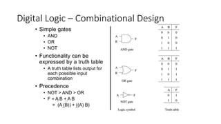
  • 1. Digital Logic – Combinational Design • Simple gates • AND • OR • NOT • Functionality can be expressed by a truth table • A truth table lists output for each possible input combination • Precedence • NOT > AND > OR • F = A B + A B = (A (B)) + ((A) B)
  • 2. Basic Concepts (cont.) • Additional useful gates • NAND • NOR • XOR • NAND = AND + NOT • NOR = OR + NOT • XOR implements exclusive- OR function • NAND and NOR gates require only 2 transistors • AND and OR need 3 transistors!
  • 3. © 2009 Pearson Education, Upper Saddle River, NJ 07458. All Rights Reserved Floyd, Digital Fundamentals, 10th ed The XOR gate produces a HIGH output only when the inputs are at opposite logic levels. The truth table is The XOR Gate 0 0 0 1 1 0 1 1 0 1 1 0 A B X A B X The XOR operation is written as X = AB + AB. Alternatively, it can be written with a circled plus sign between the variables as X = A + B. XOR and XNOR Gates
  • 4. Digital Logic Design using MOS • An nMOS transistor can be modelled as a switch connected between the drain (D) and source (S) and the switch is controlled by gate (G). • nMOS as a Switch • When the Gate (G) is Logic High (H), • the nMOS is ON • the switch is closed • D is connected to S • When the Gate is Logic Low (L), • the nMOS is OFF • the switch is open • D is disconnected from S. • An nMOS can pass the logic low (Gnd) perfectly but cannot pass logic high perfectly. • pMOS as a Switch • When the Gate (G) is Logic Low (L), • the pMOS is ON • the switch is closed • D is connected to S. • When the gate is Logic HIGH (H), • the pMOS is OFF • the switch is open • D is disconnected from S. • A pMOS can pass logic high (VDD) perfectly but cannot pass logic low perfectly. nMOS as a Switch pMOS as a Switch pMOS (VGS) Logic 0: ON Logic 1: OFF nMOS (VGS) Logic 0: OFF Logic 1: ON
  • 5. CMOS Design Methodology • Logic Design using CMOS Logic: For a given Boolean Expression, the basic CMOS design methodology involves three steps: • Step1: Take the complement of Boolean Expression • Step2: Design PDN by realizing • AND terms using series- connected nMOS • OR terms using parallel- connected nMOS • Step3: Design PUN just reverse (or dual) of the PDN • For Ex: NOT-AND (NAND) & NOT-OR (NOR) Logic
  • 6. Design of CMOS Inverter (NOT) Gate • CMOS Inverter • A CMOS inverter is the simplest logic circuit that uses one nMOS and one pMOS transistor. The nMOS is used in PDN and the pMOS is used in the PUN. • When input is LOW, the nMOS is OFF and the pMOS is ON. Hence, the output is connected to VDD through pMOS. • When the input is HIGH, the nMOS is ON and the pMOS is OFF. Hence, the output is connected to the GND through nMOS. • Load Capacitor • A capacitor is connected at the output node to represent the load seen by the inverter. • The load capacitor is charged to VDD through pMOS when the input is low and is discharged to the GND through nMOS when the input is high.
  • 7. Design of Two-Input NAND Gate • Two input NAND Gate design using CMOS Inverters, • Step 1: Take Complement of Y, • Step 2: Design the PDN. • In this case, there is only one AND term. • So, there will be two nMOS in series. • Step 3: Design the PUN. • In PUN, there will be two pMOS in parallel. Practice Example
  • 8. Design of Two-Input NOR Gate Practice Example
  • 9. Practice Examples • Question: Find the Output of the following CMOS Logic Gates. OUT= [(A.B)+C+D]’ VDD OUT= [(A.B)+C]’ F OUT= (A.B.C.D)’ Output C= (A.B)’ Output C= (A+B)’