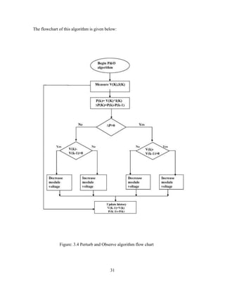
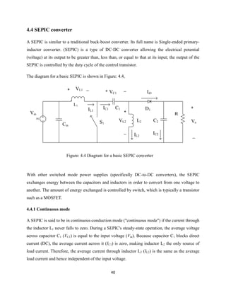
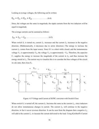
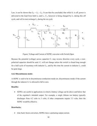
This document describes a thesis that aims to design and simulate a simple but effective charge controller with a maximum power point tracker for a photovoltaic system. It provides theoretical studies of photovoltaic systems, modeling techniques using equivalent electric circuits, and various MPPT algorithms and control methods. P-Spice and MATLAB simulations verify the design of a DC-DC converter and hardware implementation. The results validate that MPPT can significantly increase the efficiency and performance of PV systems.


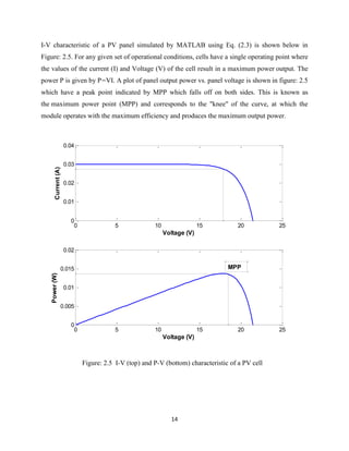
![13
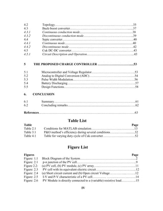
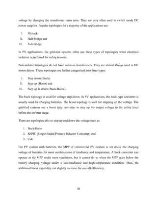
The current-voltage relationship of a PV cell is given below:
- …………………………………….. (2.1)
= [ ]…………………………….… (2.2)
From equation (1) and (2) we get,
= - [ ]……………………….……. (2.3)
Where, = output current (A)
= short circuit current (A)
= reverse saturation current (A)
= voltage (V) across the diode
q= electron charge (1.6x C)
k= boltzmann’s constant (1.381x J/K)
T= junction temperature (K)
n= diode ideality factor (1~2)
The reverse saturation current can be calculated by setting = , I=0 and n=1.6
= – 1…………………………………… (2.4)
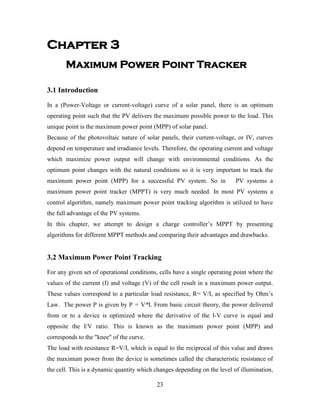
In PV panel 36 cells are connected in series. Following specifications as mentioned at the back
of the panel were used for calculation. n=1.6 has been used for the calculation.
Table 2.1
Isc (A) Vocm (V) T (K)
1.25 21.9 298](https://image.slidesharecdn.com/codientu-180501080259/85/Codientu-org-design-of-a-charge-controller-circuit-20-320.jpg)
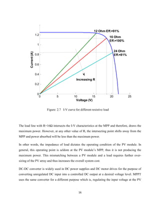
![15
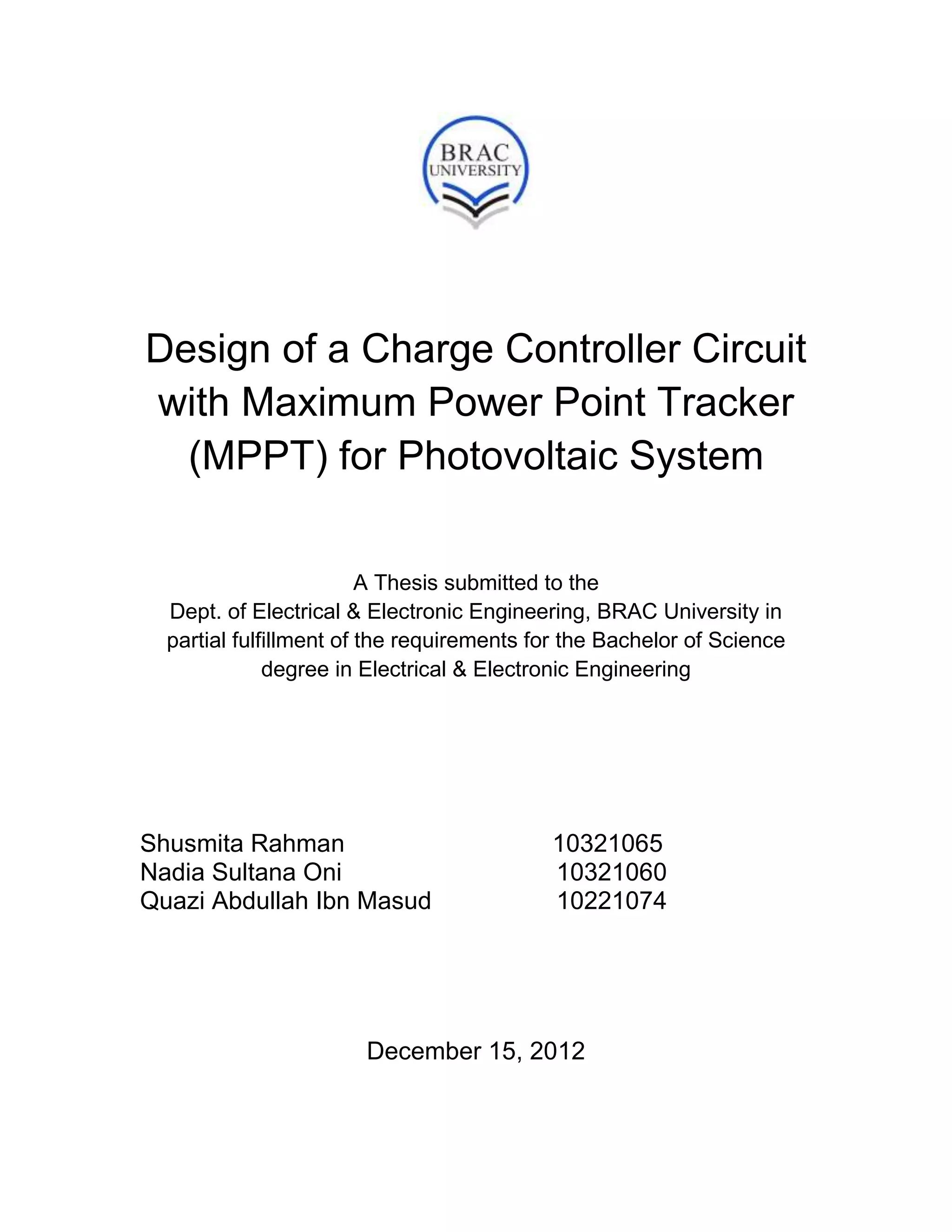
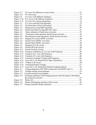
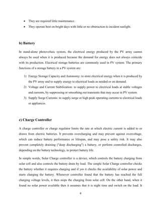
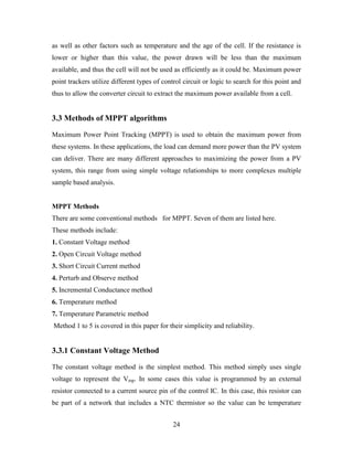
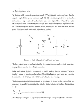
2.5 I-V curve with load resistor
When a PV module is directly coupled to a load, the PV module’s operating point will be at the
intersection of its I–V curve and the load line which is the I-V relationship of load. For example
in Figure: 2.6, the load current,
……………………………….. (2.5)
Figure: 2.6 PV module is directly connected to a (variable) resistive load
For PV panel,
= - [ ] ................................. (2.6)
Plot of equation (2.5), shown as the load line, intersects the I-V characteristics of the P-V
module, plotted using (2.6), at different points determined by the load resistance R.
The intersection determines the operating voltage and current and the power delivered to the load
R. Figure: 2.7 shows load lines drawn for three different values of load resistance R. As it can be
seen,](https://image.slidesharecdn.com/codientu-180501080259/85/Codientu-org-design-of-a-charge-controller-circuit-22-320.jpg)
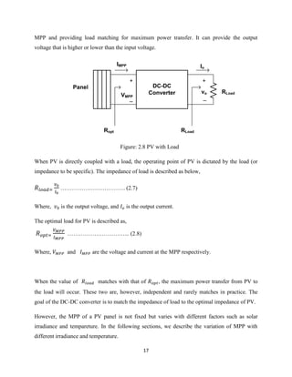


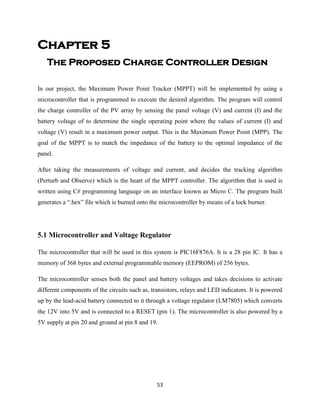
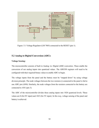
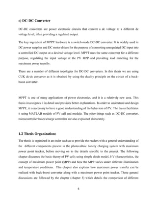
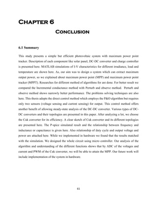
![55
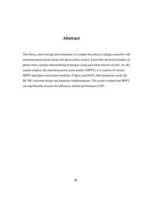
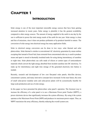
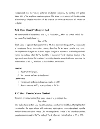
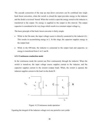
Figure: 5.2 Voltage sensing circuit diagram.
Current Sensing:
To read the current supplied by the PV module, a shunt resistor is placed in series with an ADC
input. This value is amplified and connected to the ADC port AN2. The shunt resistor gives a
voltage that is proportional to the current, e.g.: if 1A gives 5mV, 10A gives 50mV. This voltage
output is then connected to another ADC port, AN2 and run in the algorithm as an input.
Conversely, a Hall effect sensor may be used. This includes HAL 710 (Hall effect sensor with
Direction Detection) and 6851, of which 6851 is more convenient. The 6851 is an integrated Hall
effect latched sensor. The device includes an on-chip Hall voltage generator for magnetic
sensing, a comparator that amplifies the Hall voltage, and a Schmitt trigger to provide switching
hysteresis for noise rejection, and output driver with pull-high resistor. If a magnetic flux density
larger than threshold βOP, D0 is turned ON (low). The output state is held until a magnetic flux
density reversal falls below βOP causing DO to be turned OFF(high) [Pi Labs]. In this way, the
sensor detects the magnetic flux produced by the analog input, and reads current as a voltage.
However, for our purpose, we have used a shunt resistor and the voltage across it amplified by
and Op-Amp and connected to the ADC pin.](https://image.slidesharecdn.com/codientu-180501080259/85/Codientu-org-design-of-a-charge-controller-circuit-62-320.jpg)


![63
References:
1. A. Khalighand O.C. Onar: Energy Harvesting-Solar, Wind, and Ocean Energy
Conversion Systems; CRC Press, 2010.
2. Photovoltaic System Engineering [2nd
Edition]
By Roger A. Messenger and Jerry Ventre
3. http://courseware.ee.calpoly.edu/~jharris/research/super_project/ao_thesis.pdf
4. http://www.ti.com/lit/an/slva446/slva446.pdf
5. http://www.archives-ijaet.org/media/15I5-IJAET0511537-COMPARISON-OF-
MAXIMUM-POWER-Copyright-IJAET.pdf
6. Power Electronics-Converters, Application and design-[2nd
Edition]
By Ned Mohan
7. Introduction to Power Electronics by Daniel W. Hart
8. http://en.wikipedia.org/wiki/Single-ended_primary-inductor_converter
9. http://en.wikipedia.org/wiki/Buck%E2%80%93boost_converter
10. Akihiro Oi, “Design And Simulation Of Photovoltaic Water Pumping System,”
California Polytechnic State University, San Luis Obispo, September 2005.
11. [39582b]: PIC16F87XA Data Sheet 28/40/44-Pin Enhanced Flash Microcontrollers,
Microchip Technology Inc., 2003.
12. Wikipedia.
13. http://www.techshopbd.com/index.php/productcategories/miscellaneous/miscellaneous/h
all-effect-sensor-6851.
14. Marzuq Rahman, et al; “Design of a Charge Controller Circuit for multilevel Solar Panels
for Solar Home System,” 2012.
15. World Academy of Science, Engineering and Technology 44 2008-A New Maximum
Power Point Tracking for Photovoltaic Systems-Mohammed Azeb
16. Batteries and Charge Control in Stand-Alone Photovoltaic Systems Fundamentals and
Application-Prepared by:James P. Dunlop, P.E.Florida Solar Energy Center1679 Clearlake
RoadCocoa, FL 32922-5703
17. Mohamed Azab, “A New Maximum Power Point Tracking for Photovoltaic Systems,”
World Academy of Science, Engineering and Technology, 44 2008.](https://image.slidesharecdn.com/codientu-180501080259/85/Codientu-org-design-of-a-charge-controller-circuit-70-320.jpg)