Download to read offline


![1
Chapter 1
1 Introduction
Concerns about global warming and climate change have recently increased the awareness
of humanity on conventional energy sources. These sources also increase the greenhouse
gas emissions which are carbon dioxide, methane, nitrous oxide, water vapour, and ozone.
Conventional types of energy generation produce many of these gases. Use of oil for
transport and use of coal for electricity generation are the main activities that contribute to
the production of greenhouse gases. The sea temperature increases and ice on poles melts.
All these indicators have urged people that a new sustainable way of energy generation and
a much more efficient way of consumption need to be developed as soon as possible [1].
Clean energy resources have recently become very important for the future energy
generation because of these concerns [2]. Solar power generation has been considerably
becoming more attractive due to their advantages among other resources. These advantages
are direct conversion from sun light into electric power, low cost maintenance, no noise
and pollution, and long operation lifespan [3]. Solar photovoltaic power generation has a
remarkable advantage among the others, which is the fact that it can be viable in small
scale applications such that every household can generate its electricity with a small
feasible investment [4]. Unlike wind turbines, there is no noise in the operation, which
enables the system to be implemented easily in communal areas. Other applications of
clean energy production may become much more feasible when they are designed in large
scales [5] [6].
However, there are some issues in green energy generation. This generation fundamentally
depend on the availability of the resources. The energy coming from these resources also
fluctuates most of the time. For example, wind is not available and blowing at the same
speed or the sun light is not intensively shining during the day. Conversely, the electricity
network demands a continuously stable and synchronized resource. Therefore, green
energy needs to be suited to the grid by converting and extracting it carefully [7] [8].
This stabilisation of the generated power has been employing power electronics devices
such as converters and inverters. For example, PV modules produce DC power but the
electricity that we use in our homes needs to be AC power. There is a need for conversion](https://image.slidesharecdn.com/4863057c-21bb-4299-b0f6-de43b89726de-151001054941-lva1-app6892/85/FINAL-REPORT-13-320.jpg)
![2
from DC to AC in order to supply the required electricity. This conversion is done by a
power electronics inverter. Furthermore, again in PV applications, there is a point that the
PV generates the maximum power that can be extracted at a certain operating condition (no
temperature and insolation change). For the extraction, a power electronics converter is
used to track the point which is called the maximum power point [9] [10].
This project includes the modelling of a maximum power point tracker. For the purpose of
the modelling, the operation of a solar cell needs to be deeply understood. As mentioned
earlier, for this tracking problem, a power electronics device called dc-dc boost converter
also needs to be analysed. The project also focuses on the design issues and the solutions.
An MPPT algorithm which is able to tackle with the operation problems will be aimed to
achieve. Matlab & Simulink will be employed to test the system. The design of the system
will include the modelling of the PV module, development of MPPT algorithm, the
modelling of the DC-DC converter to run the algorithm with. The concept shown below
will be used to develop the system. The figure below shows the implementation concept of
PV system but the same logic can be used for the simulation .
Figure 1: The design concept of the PV system](https://image.slidesharecdn.com/4863057c-21bb-4299-b0f6-de43b89726de-151001054941-lva1-app6892/85/FINAL-REPORT-14-320.jpg)
![3
Chapter 2
2 Issues in the Development of PV Systems
The electrical power need in space applications in 1950s initially brought PV into
consideration. Cost was not important in those applications where performance was much
more crucial. PV remained back in the market since fossil fuel costs were considerably
low. However, PV and other renewable resources have become more important in the last
decade due to the fluctuations and uncertainties in the fossil fuel market [7] .
Cost reduction is the key to the development and the future of PV market. Efforts in 1970s
reduced the cost of PV for terrestrial applications to $20/Wp. Currently, the cost of
crystalline silicon modules has been reduced to around $4/ Wp. The cost has been reduced
up to $1/ Wp for grid-connected applications. These values can also go further down with
mass production of the PV modules. Large PV manufacturing plants with the capacity over
500MWp /y can reduce the cost to $1/Wp [7] [11].
The cost of PV systems consists of the module cost and the Balance-of-System (BOS)
components. BOS includes power conditioners, converters, wiring, and inverters.
Currently, BOS is considered to be around $3-4/ Wp without storage system. This can be
reduced to $1/ Wp with further R&Ds [7] [12].
Another issue is the battery storage system for stand-alone or sometimes grid-connected
systems. The cost of storage system is added to BOS. The size of storage system is
important in order to calculate the cost which increases proportional to the increasing size
of the system. For instance, in a sunny area with approximately 4-5 peak hours of sunlight,
around 15kWh per kWp of battery capacity might be required to store the energy for 3-4
days. A typical lead-acid battery for this kind of system would cost around $150-200/kWh.
The life-time of the battery is also important in terms of the cost. PV modules have longer
life-time than batteries. The cost of storage increases in less sunny areas since more storage
capacity is needed. High battery costs, weight and required space for storage, and also
maintenance are important issues in such kind of systems [7].
Profitability is considerably an important effect on the growth of PV industry as in every
industry. The entire cost of a PV system includes manufacturing costs, marketing costs,](https://image.slidesharecdn.com/4863057c-21bb-4299-b0f6-de43b89726de-151001054941-lva1-app6892/85/FINAL-REPORT-15-320.jpg)
![4
sales taxes and import duties, and also distributors’ costs and profits. All these factors
affect the PV investments by private companies or individuals. Many countries have
introduced taxes or regulatory agreements such as feed-in-tariffs and government subsidies
to attract the renewable investments as the concerns on global warming and climate change
grow considerably in the world [7].](https://image.slidesharecdn.com/4863057c-21bb-4299-b0f6-de43b89726de-151001054941-lva1-app6892/85/FINAL-REPORT-16-320.jpg)
![5
Chapter 3
3 Principles of Solar Cell Operation
The operation of a solar cell relies on the working principle of semiconductors which can
directly convert sunlight into electricity with the help of photovoltaic effect. The operation
principles of all solar cells are essentially the same. They all use a basic structure including
a junction between two different materials and an electric field exists across these
materials. Electrons and holes, which cause a flow in opposite directions across the
junction, are generated with the absorption of light. A flow of direct current power is
obtained by this flow of absorbed photons [13] [7].
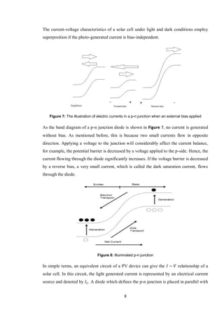
Figure 2: The essential features of a Si solar cell [7]
The photovoltaic effect can be observed on a crystalline silicon solar cell which possesses
a good model and a simple junction structure which can be seen in Figure 2.
Figure 3: Illustration of band diagram of semiconductors
The quantum theory defines the energy levels of an electron in the crystal form as within
the bands. The valence and conduction bands are separated by the band gap which is the](https://image.slidesharecdn.com/4863057c-21bb-4299-b0f6-de43b89726de-151001054941-lva1-app6892/85/FINAL-REPORT-17-320.jpg)
![6
energy difference between these two bands and it is usually denoted by . If there are no
electrons in the conduction band and the valence band has correct number of electrons,
such semiconductor is called as intrinsic since it is a pure structure. There are two ways for
a semiconductor to be able to conduct electricity, which either the carriers are moved to the
conduction band or removed from the valence band. This is achieved by doping which is
the formation of a semiconductor with an impurity.
Figure 4: Cross section of a p-n junction solar cell [7]
Figure 4 shows the double electrical layer with ionised dopant atoms (+,-) in the junction
and the two depletion regions (DRs) with equal and opposite quantities of junction charge
together with the base-layer quasineutral region.
Figure 5: Generation and movement of electrons and holes in a p-n junction solar cell [7] [14]](https://image.slidesharecdn.com/4863057c-21bb-4299-b0f6-de43b89726de-151001054941-lva1-app6892/85/FINAL-REPORT-18-320.jpg)
![7
When the energy of absorbed photons is greater than the band-gap energy of silicon,
electrons move from valance band to the conduction band. This generates electron-hole
pairs in the illuminated part of the cell. These electron-hole pairs quickly turn into
independently moving free electrons and holes. Free electrons move from the p side to the
n side and the holes from the n side to the p side because of the effect of the built-in
electric field.
Figure 6: A p-n homojunction cell under illumination at open circuit and short circuit relatively [7].
The generation of photocurrent and photovoltage occurs when a photovoltaic cell is
illuminated. When the photons whose energy bigger than the bad-gap energy of the
semiconductor are absorbed, the minority carries are generated inside the illuminated
region of the cell. The intensity of illumination inside the cell exponentially drops through
the distance across the cell but it can usually penetrate into the base layer of the cell. The
behaviour of the photo-generated minority carriers under illuminated cell is similar to
much smaller populated thermally generated minority carriers inside the dark cell. These
minority carriers are swept across the junction because of the strong junction field.
The photo-generation currents in Figure 6 are increased by the photo-
generated minority carriers. is the photo-generated electrons flowing from the p side to
the n side of the junction and is the photo-generated holes flowing from the n side to
the p side of the junction. The overall photocurrent is the sum of these two currents
denoted as . The photo-generated current is proportionally dependent on the absorption
of photon flux. No current is produced in the cell at open circuit and the recombination
current provides the balance of photo-generated current. The Figure 6 shows the
difference between the Fermi levels of the two junctions denoted by . The picture on
the left-hand side in Figure 6 shows the operation of an illuminated cell under short-circuit
condition where maximum current is generated in the cell but the output voltage is zero.](https://image.slidesharecdn.com/4863057c-21bb-4299-b0f6-de43b89726de-151001054941-lva1-app6892/85/FINAL-REPORT-19-320.jpg)
![10
Chapter 4
4 Maximum Power Point Tracking (MPPT)
PV systems are typically non-stable power supply as generated power from photovoltaics
is dependent on the irradiance and environmental temperature factor [15]. The invention of
p-n junction in 1950s introduced the famous nonlinear relationship between the current and
voltage of a solar cell. The photoelectric current generates power according to the voltage
drop across the junction. In this non-linear v-i, there is a point that maximum power occurs
during operation with maximum efficiency, the so-called maximum power point (MPP). It
develops when the rate if change of the power with respect to the voltage equals to zero.
This tracking is called maximum power point tracking (MPPT). The analytical solution of
MPPT is hard to achieve because of the complicated nonlinear relationship of V-I and
hence P-V when the irradiance and temperature vary. Therefore many methods have been
improved for MPPT [16] [17]. These techniques are; the Perturb and Observe (P&O),
modified P&O, the Incremental Conductance (IC), Constant Voltage (CV), Short Current
Pulse, Open Circuit Voltage, IC and CV combined, and the Temperature Methods. There
are some more methods such as Fuzzy Logic, Sliding Mode, and the Artificial Neural
Network. These methods can be considered in terms of many aspects including simplicity,
convergence speed, sensors, cost, and parameterization, etc. [17] [18].
4.1 Common MPPT Types
Many algorithms have been proposed in the literature for maximum power point tracking.
These algorithms show differences in terms of implementation such as digital or analogue,
tracking speed, accuracy in tracking, complexity, oscillation around the maximum power
point, etc. [19]. These algorithms will be described with their advantages and
disadvantages in this section.
4.1.1 Hill Climbing/Perturb and Observe (P&O)
These two algorithms are different ways of implementing the same method. The duty ratio
of the converter is used in hill-climbing method and P&O includes a perturbation in the
power output of the PV array. For a PV array, perturbation of the duty ratio of power
converter also perturbs the current and eventually the voltage of the PV array [20].](https://image.slidesharecdn.com/4863057c-21bb-4299-b0f6-de43b89726de-151001054941-lva1-app6892/85/FINAL-REPORT-22-320.jpg)
![11
The P&O algorithms periodically apply increase or decrease on the terminal voltage. This
influences the power output. The voltage is changed in the same direction if the power
increases or in the inverse direction if the power decreases based on the sign of the dP/dV.
It has commonly been used and it is an iterative method.
The steps of the method are simply;
1. Measure the current and voltage, calculate the power.
2. If the power is constant, measure the values again.
3. If the power decreases or increases, determine the voltage direction.
4. Modify the current due to the direction [21] [22].
Figure 11: Flow Chart of P&O Algorithm [23]](https://image.slidesharecdn.com/4863057c-21bb-4299-b0f6-de43b89726de-151001054941-lva1-app6892/85/FINAL-REPORT-23-320.jpg)
![12
Figure 11 shows the general flow chart of P&O. PV system is disturbed by periodically
reducing or raising a fixed step size ( of the array voltage . If the power output
increases to the MPP, the following perturbation happens in the same direction and
the opposite. A proper step size should essentially be chosen. A large step size causes
oscillations around the MPP and waste of some energy. Conversely, a small step size slows
down the response to the irradiance variations [23] [24].
4.1.2 Incremental Conductance (IC)
The algorithm is used to overcome the limitations of the P&O with the help of array’s
incremental conductance to calculate the sign of dP/dV without a perturbation. At the
MPP, dP/dV=0, it is thus possible to say that the following condition occurs;
( ) ( )
In other words, the method uses the slope of derivative of current with respect to the
voltage to obtain the MPP.
If the operating point is on the right side of the MPP, the following happens;
( ) ( )
If the operating point occurs on the left side of the MPP;
( ) ( )
Therefore, the IC can calculate that the tracking has reached the MPP and stop perturbing
the operation point.
If the condition does not occur, the algorithm increases or decreases Vref to find the new
MPP. The increment size indicates the speed of MPPT.
Using the method it is theoretically possible to observe when the MPPT occurs [18] [25].](https://image.slidesharecdn.com/4863057c-21bb-4299-b0f6-de43b89726de-151001054941-lva1-app6892/85/FINAL-REPORT-24-320.jpg)
![13
4.1.3 Fractional Open Circuit Voltage
This algorithm assumes that the MPP voltage varies slightly with the changing irradiance.
The value of VMPP/VOC is dependent on the solar cell parameters but the value of 76% is
commonly used. The algorithm sets the PV current to zero to measure the VOC. Then the
operating voltage of the array is set to 76% of the open circuit voltage regardless the
irradiance or cell temperature. This method works faster than the others but the problem is
that the load is disconnected each time to measure the open circuit voltage and the energy
available at this time is wasted. To prevent this, some pilot cells can be used to measure the
VOC. These must be selected carefully to show the close characteristics that the array has.
Moreover, MPP does not always occur at 76% of VOC [25] [26].
4.1.4 Fractional Short Circuit Current
Under changing conditions, IMPP is approximately linearly dependent on the ISC of the
array.
Figure 12: Flow chart of Incremental conductance [22]](https://image.slidesharecdn.com/4863057c-21bb-4299-b0f6-de43b89726de-151001054941-lva1-app6892/85/FINAL-REPORT-25-320.jpg)
![14
(4.1)
must be obtained according to the PV array used. is generally between 0.78 and 0.92.
However, measurement of is problem during operation. A switch has to be added to the
converter to short circuit the array periodically and it can therefore be sensed by a current
sensor. This has an impact on cost because of the additional components. There is a
decrease in power output because of the measurement of and the MPP can never
perfectly obtained since it is not always suitable in the Eq.1 above [20].
4.1.5 Constant Voltage (CV)
This is the simplest method in MPPT. The operation point of the PV array is tried to be
stabilised near the MPP by comparing it with a fixed reference voltage which equals
to the voltage at MPP according to the module characteristics or another best
voltage value. It is assumed that the atmospheric conditions are not significant on the
. When in low irradiance conditions, this method works more effectively than the
either P&O or the IC and this method is sometimes combined with other techniques [18]
[21].
Figure 13: Flow chart of Constant Voltage](https://image.slidesharecdn.com/4863057c-21bb-4299-b0f6-de43b89726de-151001054941-lva1-app6892/85/FINAL-REPORT-26-320.jpg)
![15
4.1.6 Fuzzy Logic Control
The development of information technology has caused new techniques in MPPT (for
example; fuzzy logic, neural network, etc.). Fuzzy logic controllers can work with
imprecise inputs and they can handle the nonlinearity. In fuzzy logic control, no
mathematical model is required. It is also implemented easily in control system [27]. The
method generally includes three stages which are fuzzification, rule base table lookup, and
defuzzification. The input is the variable ratio of power to current or voltage. Fuzzification
process includes the conversion of numerical input variables into linguistic variables
according to a membership function [28]. The input variables are the error E and the
change in the error CE.
Figure 14: General diagram of a fuzzy [29]
P(k) = instantaneous power of the PV generator.
E(k) = indicates the operation point of the load at the instant k whether it locates on the
right or the left of the MPP. CE(k) = shows the direction of this point.
Mamdani’s method is used to carry out the fuzzy inference and the centre of gravity is used
to compute the output of FLC in the defuzzification. The output is the duty cycle;
∑ ( )
∑
and fuzzy sets used in the fuzzy control rules are defined as;
On the other hand, because of the quickly varying environment of PV systems,
conventional fuzzy logic controllers cannot show a quick and efficient performance in
transient conditions. Therefore, the rules need to be adapted for the changeable
environments. For these kinds of environments, some modified methods have been studied](https://image.slidesharecdn.com/4863057c-21bb-4299-b0f6-de43b89726de-151001054941-lva1-app6892/85/FINAL-REPORT-27-320.jpg)
![16
for an accurate and rapid MPP tracking such as Dual-mode Fuzzy Control algorithm,
Asymmetric Fuzzy Control, or Neural and Fuzzy together [30].
NB=Negative big, NS=Negative small, ZE=Zero, PS=Positive small, PB=Positive big.
Table 1: Fuzzy Rule Table [29]
CE
E NB NS ZE PS PB
NB ZE ZE PB PB PB
NS ZE ZE PS PS PS
ZE PS ZE ZE ZE NS
PS NS NS NS ZE ZE
PB NB NB NB ZE ZE
A fuzzy logic controller is defined above by the help of [29].
Figure 15. Membership for inputs and outputs](https://image.slidesharecdn.com/4863057c-21bb-4299-b0f6-de43b89726de-151001054941-lva1-app6892/85/FINAL-REPORT-28-320.jpg)
![17
4.1.7 Neural Network
Neural networks can potentially provide an improved method of non-linear models. Neural
networks are capable of self-adaption so that they can deal with the non-linearity,
uncertainty and parameter changes [31].
Neural networks contain three stages: input, hidden, and output layers. The Input variables
can be open circuit voltage, short circuit current, irradiance, and temperature or a
combination of them. The output can be the duty cycle signal for the power converter. The
closeness of the operation point is dependent on the algorithm used in the hidden layer. All
the links are weighted. The link between the nodes i and j are shown as a weight of wij .
The PV array is tested for a long time for the purpose of this method by obtaining the
combination between the inputs and outputs. A neural network must be trained for each
individual PV array as they have different characteristics. These characteristics also change
with time. Therefore, the neural network must periodically be trained to achieve the
accurate MPPT [20].
A method has been proposed in papers [31] [32] called “Back propagation neural
networks”. Back propagation neural networks are used as pattern classifier and an example
of non-linear layered feed-forward networks. It provides universal approximations to non-
linear input-output mapping. The back propagation algorithm is a computationally efficient
method for the training of multilayer perceptron and it may be viewed as implementation
of an optimization method known as stochastic approximation. This algorithm is used for
training. It only needs inputs and the desired output for the adaptation of weight.
Figure 16: Example of neural network](https://image.slidesharecdn.com/4863057c-21bb-4299-b0f6-de43b89726de-151001054941-lva1-app6892/85/FINAL-REPORT-29-320.jpg)
![18
4.2 Comparison of Common MPPT Types
The MPPT types described and analysed in above sections are briefly compared in the
following table with their relative speed, complexity, reliability, and implementation.
Table 2: Comparison of common MPPT Types [2]
MPPT technique Speed Complexity Reliability Implementation
Fractional Short Circuit Medium Medium Low Digital/Analog
Fractional Open Circuit Medium Low Low Digital/Analog
Incremental Conductance Varies Medium Medium Digital
Hill Climbing Varies Low Medium Digital/Analog
Fuzzy Logic Fast High Medium Digital
Neural Network Fast High Medium Digital
4.3 Other MPPT Types
Apart from the common types mentioned above, there are various MPPT types in the
literature, especially some for a specific type of applications. Followings are some of
which can be used for MPPT but not very common in the literature.
4.3.1 Ripple Correlation Control (RCC)
Ripple Correlation Control (RCC) is a fast, robust online and dynamic optimization
technique which can be adapted for an MPPT or for motor efficiency maximization.
RCC employs the ripple which every switching power converter has and uses it to observe
the operation point [33]. It is objectively used to maximise or minimise a cost function,
such as power or energy value in an MPPT implementation. RCC employs information in
Figure 17: PV array connected to boost converter [37]](https://image.slidesharecdn.com/4863057c-21bb-4299-b0f6-de43b89726de-151001054941-lva1-app6892/85/FINAL-REPORT-30-320.jpg)
![19
the inherent switching ripple to calculate the gradient of the cost function. Consequently,
information available on the fast time scale of voltage and current ripple activates the
control to obtain a slow time scale objective, operation at the optimum [34].
General features of RCC for MPPT [35];
- Converges asymptotically to MPPT
- Employs array voltage and current ripple, which have to exist if a switching
converter is employed, to obtain the gradient information, artificial perturbation is
not needed
- Attains convergence at a rate limited by switching period and the controller gain
- Does not depend on assumptions or characterization of the module or a single cell
- Able to compensate the module capacitive effects
- Have several circuit implementations (digital, analogue, etc.)
- Well-developed theory
The inductor current and array power can be correlated to determine if is above or
below . Considering the behaviour of changes in power and current, take the value
equal to where C=0, which is the parasitic capacitance of the array. From Figure 18, if
is below , a current ripple exposed along the curve results in an in-phase power ripple;
which means; ( ⁄ ) and ( ⁄ ) are positive. Conversely, if is above , the
current and power ripple become out of phase, which means; ( ⁄ ) and ( ⁄ ) are
negative. If these are combined as [36];
Figure 18: PV array average power vs. average inductor current](https://image.slidesharecdn.com/4863057c-21bb-4299-b0f6-de43b89726de-151001054941-lva1-app6892/85/FINAL-REPORT-31-320.jpg)
![20
In eq.4.2, if increases when the product is greater than zero, and decreases, ought to
approach . To do this the product can be integrated;
∫
d is the duty cycle and k is a constant, positive gain. The inductor current decreases and
increases with the duty cycle. Therefore, adjustment of d can give the correct movement of
.
In eq.4.3, derivation of signals is used, which can be measured directly. This might cause
problems in power conversion circuits, which needs to be handled.
Alternatively, eq.4.3 can be proposed with a different approach. The optimal set point
develops when ; hence the control law
∫
Is expected to work as the integrand can approach zero while approaches . (4.4) is not
generally a signal which is available in a real circuit. unless the convergence is made
slowly, the achievement of signal-to-noise ratio of (4.4) is difficult.
The speed and trajectory of convergence can be changed by scaling the integrand of (4) by
a positive number but it still converges. If the integrand is scaled by , which is
positive as long as changes;
∫ ( ) ∫
This is the same as eq.3 but calculated from a different view. will be driven to zero by
this integral law [37].
RCC can be distinguished from traditional P&O with the asymptotic convergence. Another
is that convergence speed is on the order of the switching frequency. RCC can be](https://image.slidesharecdn.com/4863057c-21bb-4299-b0f6-de43b89726de-151001054941-lva1-app6892/85/FINAL-REPORT-32-320.jpg)

![22
When is computed after current sweep, (4.12) can be employed to control if the MPP
is reached.
This method has been implemented several times. The paper in [20] describes all the steps
above and then points out that this method can be feasible if the power consumption of the
tracking unit is lower than the increase in power.
4.3.3 dP/dV or dP/dI Feedback Control
The reference [20] claims that another way for MPPT is to compute the slope of
the PV power curve and use a feedback to the power converter with using a control to drag
it to zero. The computation of the slope is different in the literature. Some computes and
saves its sign and using the sign, the duty cycle of power converter is decreased or
increased to obtain the MPP. Some uses a linearization based on the computation of .
Some use data conversion and sampling with digital division of voltage and power to
obtain .
4.3.4 DC Link Capacitor Droop Control
This method is specifically designed to be used in a PV system connected with an AC
system in parallel [20].
The duty ratio of a boost converter;](https://image.slidesharecdn.com/4863057c-21bb-4299-b0f6-de43b89726de-151001054941-lva1-app6892/85/FINAL-REPORT-34-320.jpg)
![23
If stays constant, rising up the current going into the inverter increases the power
coming from the boost converter and therefore the power from the array. can be
retained constant as long as the power of the inverter does not exceed the maximum power
available from the array as the current is rising up. Otherwise, begins to droop. At that
point, becomes maximum and the array operates at the MPP [20].
4.3.5 Load Current or Load Voltage Maximization
The idea of the MPPT is to maximise the output power of the PV array. For a power
converter connected to a PV array, maximising the array power maximises the power
output of the load of the power converter and the opposite should be possible in the case of
lossless converter.
Most loads can be voltage source type, resistive, current source, or combined of all of
these. The load current should be maximised for a voltage-source type load to obtain
the maximum power output. The load voltage should be maximised for a current-
source type load for the maximum power output. The load current or the load voltage can
be maximised to maximise the load power.
For a battery used PV system, the load is most of the time is the battery which can be
considered as a voltage-source type load. Therefore, the load current can be used as the
control signal [20].](https://image.slidesharecdn.com/4863057c-21bb-4299-b0f6-de43b89726de-151001054941-lva1-app6892/85/FINAL-REPORT-35-320.jpg)
![24
Chapter 5
5 MPPT under Partially Shaded Conditions (PSC)
All these MPPT schemes which have been mentioned are suitable under normal weather
conditions and they are not able to operate under partially shaded conditions as the output
of a PV module is low (around 20-35V). Therefore, a number of modules are connected in
series in order to obtain a suitable DC voltage output [38]. This is denoted as string.
However, when some of the modules in the array are shaded, MPPT becomes a difficult
task. Under this partially shaded condition, a reduction in the total output power of the
modules occurs and because of the unbalanced generation caused by unbalanced
insolation, multiple MPPs can be observed on the P-V characteristic. The conventional
MPPT methods can fail to track the global MPP since they may tack the local MPPs. This
might result in reduction in the generated power output and hence the efficiency will
decrease [39].
5.1 The Characteristics of PV Array under Partially Shaded
Conditions
A PV array is designed with several PV modules to obtain the suitable voltage and current
for the purpose. The array design issues are firstly to protect the modules from hot-spot,
which is a module in series in the array less illuminated than the others and hence affects
the power generated by the rest of the modules, bypass diodes are connected in parallel
with each module in the array. Secondly, blocking diodes are used to protect the modules
from the potential difference between the strings [40].
5.2 MPPT Failures under PSC in Conventional Methods
Traditional MPPT types have a good efficiency over 99% under the uniform irradiance.
However, this might decrease under partially shaded conditions due to the multiple local
MPPs. The reason of the tracking failure can be observed in Figure 20. It is shown that the
MPP is on point A before PSC. MPP moves to point B after PSC. However, the real MPP
is in this case on point C. Since the traditional methods follow the operation point by](https://image.slidesharecdn.com/4863057c-21bb-4299-b0f6-de43b89726de-151001054941-lva1-app6892/85/FINAL-REPORT-36-320.jpg)
![25
changing it with a fixed predetermined step size, the operation occurs around point B, but
the power available between point C and B is lost because of the MPPT failure. Therefore,
the operating point has to be moved to point C by modifying the MPPT algorithm [41].
Figure 20: MPPT failure under PSC [41]
Figure 19: Array design and the I-V & P-V Characteristics [41]](https://image.slidesharecdn.com/4863057c-21bb-4299-b0f6-de43b89726de-151001054941-lva1-app6892/85/FINAL-REPORT-37-320.jpg)
![26
In relatively high levels of shadow, the output voltage of the shaded PV module is still
available, where each module should not work on their own MPP and the output current of
overall array is decreased. However, the failure should not happen as there is one MPP. On
the other hand, in relatively low shadow levels, the bypass diode might be working. The
bypass diode is conducted if the module is reverse biased. This happens if two conditions
are available, firstly the mismatch between the module, and secondly if the output is short
circuit. The multiple local maxima can be illustrated on the P-V characteristic in this case
[40].
Multiple Local Maxima
As mentioned before, the multiple local maxima can be very fundamental in the operation
of the system. There might be a considerable power loss of the local MPP is tracked
instead of the real MPP. The current sweep and the state-based methods can handle the
multiple local maxima and track the true MPP. However, other methods need some
modifications in the algorithm [20].](https://image.slidesharecdn.com/4863057c-21bb-4299-b0f6-de43b89726de-151001054941-lva1-app6892/85/FINAL-REPORT-38-320.jpg)
![27
Chapter 6
6 Modelling of PV Module
The basic model of a PV module does not describe the I-V characteristic of a practical PV
module. Practical modules consist of several solar cells connected in series and parallel and
additional parameters are needed to demonstrate characteristic. There are a few proposals
of a solar cell equivalent circuit in the literature. These are “Four Parameters Model” and
“Five Parameters Model” [42].
Four Parameters Model describes the operation of a photovoltaic module on condition that
the values of form factor, series resistance of the cell, diode saturation current, and the
photo electric current which relates to a given radiation and temperature. These values can
be obtained as a function of data from the datasheet that manufacturers supply [43].
Figure 21: Four parameters model
Figure 22: Five parameters model](https://image.slidesharecdn.com/4863057c-21bb-4299-b0f6-de43b89726de-151001054941-lva1-app6892/85/FINAL-REPORT-39-320.jpg)
![28
Five Parameters Model has a shunt resistance different from the four parameters model.
This is added to demonstrate a more accurate model for solar cell. The effects of loss
resistances will be mentioned later [44].
6.1 Mathematical Model of Solar Cell
Kirchhoff Law is applied in the five parameters model shown in Figure 22. Hence,
is given by Shockley equation:
* ( ) +
In equation (6.2), thermal voltage of a cell is described as [45];
Hence, equation (6.2) becomes;
* ( ) +
[ ]
[ ]
[ ]
[ ]
[ ]
( [ ])](https://image.slidesharecdn.com/4863057c-21bb-4299-b0f6-de43b89726de-151001054941-lva1-app6892/85/FINAL-REPORT-40-320.jpg)
![29
[ ]
Substitute the eq.6.2 and 3 into eq.6.1. Hence, [43] [46] [47] [48]
* ( ) +
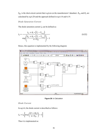
If the short circuit conditions are applied to eq.6.4, can be obtained:
[ ( ) ]
The term with is very small, eq.6.5 is mostly simplified:
If the open circuit conditions are applied to eq.6.4, can be obtained:
[ ( ) ]
If eq.6.5 is substituted in eq.6.7,
( )
Crystalline silicon PV modules possess a form factor ( ) between 1 and 1.3 in their
mathematical model. The value of is taken to be 1 in this model [45].
Different combinations of form factor, series resistance, and shunt resistance are supported
in eq.4. The I-V curves develop on the same points of short circuit current, voltage and
current at MPP, and open circuit voltage. Those occurs on a given temperature and
irradiance [49].
The simulation can be easily done when the all parameters of the module are obtained.
However, some parameters are not given in the datasheets of manufacturers. These
parameters are light-generated or photovoltaic current, the series and shunt resistances, the
diode form factor, the diode reverse saturation current and the band-gap energy of the](https://image.slidesharecdn.com/4863057c-21bb-4299-b0f6-de43b89726de-151001054941-lva1-app6892/85/FINAL-REPORT-41-320.jpg)
![30
semiconductor. They need to be evaluated using the given data and with the help of
mathematical equations as well as maximum power point condition. They only present
some experimental data about electrical and the thermal characteristics of the arrays. These
are the open circuit voltage , the short circuit current , the voltage at MPP ,
the current at MPP , the open circuit voltage/temperature coefficient , the short
circuit current/temperature coefficient , and the maximum peak power . These
values are obtained under standard test conditions (STC) of irradiation and temperature
[48].
6.2 Analysis of the Mathematical Model
Loss resistances (series and shunt resistance) have some effects on the I-V curve. They
both lead to the degradation of the curve. The current that passes through the shunt
resistance results in the part of the I-V curve running from short circuit to the proximity
whereas the series resistance brings about greater voltage drops between the open circuit
voltage and the voltage at maximum power point [50].
With the help of given values of which are available in the datasheets
of manufacturers and using the model and the previously derived equations, series and
shunt resistances can be obtained [51].
At the MPP the following condition occurs:
In the eq.6.4 if is derived with respect to :
* ( )+
If the equations 6.9 and 6.10 are compared:
* ( )+
Because of the existence of the exponential term and , the effect of loss resistances
cannot effectively be analysed by eq.6.10.](https://image.slidesharecdn.com/4863057c-21bb-4299-b0f6-de43b89726de-151001054941-lva1-app6892/85/FINAL-REPORT-42-320.jpg)
![31
6.2.1 Calculation of Equation for
The equation for can be obtained after some approximations and substitution of into
eq.11 which can be used to investigate the effect of loss resistances.
Using eq.6.4 and 6.6, after some approximations, happens to be:
* + ( )
Now (eq.6.12) can be substituted in eq.6.11:
* + * +
Considering the fact that , eq.6.13 can be even more simplified:
* + [ ]
Here;
are always true. The brackets are therefore positive, which
allows the fact that is reduced if increases. Since , is
always negative. Hence, decreases with the decreasing .
6.2.2 Calculation of Equation for
In order to observe the effect of both series and shunt resistances on , firstly eq.4 and
eq.11 can be equated and by some simplifications:
[ ( ) ]
If and in eq.6.5 and 6.8 are substituted in eq.6.15 above and after some
rearrangements, following is obtained:
* + [ ] ( )
Then if the logarithm of eq.6.16 is taken:](https://image.slidesharecdn.com/4863057c-21bb-4299-b0f6-de43b89726de-151001054941-lva1-app6892/85/FINAL-REPORT-43-320.jpg)
![32
* ( ) ( )+
Here in this equation, the effect of and is lower than in the first
logarithmic term. Further logarithm of this term makes it even smaller. Therefore the effect
of series resistance in this term is limited. If it is considered that is high enough, the
second logarithmic term goes to 0. Hence the equation simply becomes:
( )
The shunt resistance less affects the . It will significantly have an effect when it is
very small. On the other hand, the series resistance considerably affects the [45] [52].
6.2.3 Determination of Series Resistance
Since the value of series resistance is not given by the manufacturers, it is necessary to
evaluate the value that the series resistance takes. It can be obtained with the help of given
values of , , and . If the eq.17 is derived to obtain , it gives:
[ ( )]
Eq.6.18 requires an iterative solution as the term is also in the logarithmic terms. To
solve this equation, initial value of is obtained by removing and from
the logarithmic term:
[ ( )]
Then the value of is inserted in the eq.6.18 to obtain . By doing it several times, the
accuracy of the result can be improved.
6.2.4 Determination of Shunt Resistance
The shunt resistance is not as critical as the series resistance. Hence it can be calculated
with less accuracy. If the series resistance is once known, the shut resistance can be
obtained by using eq.6.14.
[ ]](https://image.slidesharecdn.com/4863057c-21bb-4299-b0f6-de43b89726de-151001054941-lva1-app6892/85/FINAL-REPORT-44-320.jpg)
![33
This equation does not require an iterative solution as the series resistance does.
6.3 Simulation of PV Module Using Matlab&Simulink
PV module is simulated in this section by using all the relevant equations above and with
the help of Simulink environment for mathematical modelling. The I-V and P-V
characteristics of PV module are aimed to obtain in order to observe the irradiation and
temperature effects [42]. It is generally assumed that in practical PV modules
since the shunt resistance is high and the series resistance is low. The light-generated
current is linearly dependent on the solar irradiation as well as being affected by the
temperature. Hence, this relationship can be defined with the following equation:
* ( )+
This can be modelled with the following Simulink diagram:
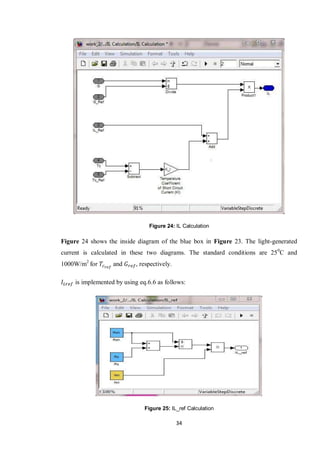
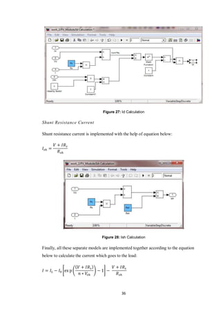
Figure 23: IL Calculation](https://image.slidesharecdn.com/4863057c-21bb-4299-b0f6-de43b89726de-151001054941-lva1-app6892/85/FINAL-REPORT-45-320.jpg)


![40
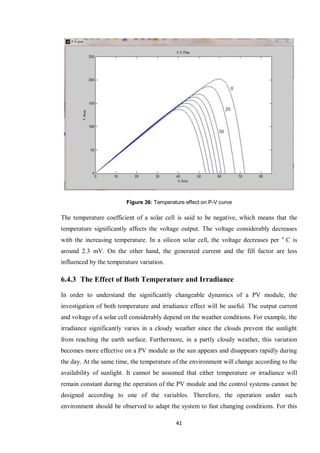
Figure 34: Irradiation effect on P-V curve
6.4.2 Temperature Effect
Cell temperature mostly affects the voltage output of the PV module. The effect of
temperature on I-V and P-V characteristics is shown in Figure 35 and Figure 36.
Temperature values from 00
C to 1000
C are applied to the module [53].
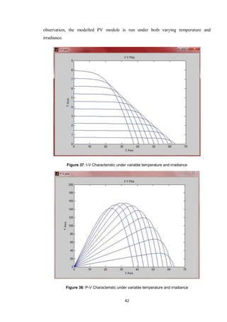
Figure 35: Temperature effect on I-V curve](https://image.slidesharecdn.com/4863057c-21bb-4299-b0f6-de43b89726de-151001054941-lva1-app6892/85/FINAL-REPORT-52-320.jpg)
![43
Chapter 7
7 DC-DC Boost Converter
The importance has been on renewable energy generation during the last decade. There are
many issues in such systems including wind, solar, tidal and wave energy. These problems
need to be analysed and solved in order to provide the smooth and suitable energy
generation for the grid and consumers. For instance, in a solar PV application, the
generated DC voltage is normally low and has to be increased before connection to the
grid. This particular problem is solved by dc-dc converters without transformers being
used in the system, which also results in higher conversion efficiencies [54].
A power electronics converter is normally used for the PV MPPT applications. As shown
in earlier sections, MPPT is, in simple terms, a power electronic device placed between the
PV module and the load to achieve to extract the maximum power from the system.
Several converter types have been implemented for MPPT design. These can be listed as
buck, boost, buck-boost, and cuk converters in the literature. The boost converter has
several advantages over the others such as higher conversion efficiency, fewer components
required for hardware design and related cost [55].
The term “boost” describes the action of increasing the source voltage to a higher voltage.
However, the primary current is required to be greater than the secondary current by a
factor of the ratio between secondary and primary voltages [56].
There is a considerable amount of theory in the background of the operation of a power
electronics converter. In this section, DC-DC boost converter will be analysed and
modelled with Matlab&Simulink.
7.1 Pulse Width Modulation (PWM)
It should be said that the operation of a circuit under PWM is beneficially essential in order
to further understand the switching converters. PWM is a control method where a transistor
operates either in on or off position. Under PWM control, the time when the transistor is
saturated, it is described as on-time and when it is driven to cut-off, it is known as off-time
[56].](https://image.slidesharecdn.com/4863057c-21bb-4299-b0f6-de43b89726de-151001054941-lva1-app6892/85/FINAL-REPORT-55-320.jpg)
![44
Figure 39: A simple circuit with a transistor and on-off conditions
When the voltage across the base and emitter of the transistor is zero ( and hence
), the transistor operates in cut-off condition and behaves as a switch opening the
circuit ( ). When , it closes the circuit and the voltage between the resistor
becomes zero [57].
Figure 40: Voltage on the resistor
Figure 40 shows the voltage on the resistor during the on- and off-time of the transistor. T
denotes the period of switching which is the sum of on- and off-time. Hence the switching
frequency becomes [58]:
As can be seen, despite being not constant, the voltage on the resistor has a DC component
of which the average value can be calculated as [59]:
∫
When the equation above is integrated [60]:](https://image.slidesharecdn.com/4863057c-21bb-4299-b0f6-de43b89726de-151001054941-lva1-app6892/85/FINAL-REPORT-56-320.jpg)
![45
It can be seen that the average output voltage is proportional to the on-time. The duty ratio
is defined as the ratio of on-time to the period T.
Eq.7.3 can be then expressed as:
The average power of the resistor can be effectively controlled linearly with the PWM
method. The RMS value of the output voltage can be calculated by [61]:
√ ∫
In terms of the duty ration, eq.7.6 becomes [62]:
√
And finally the average power on the resistor:
7.2 Analysis of DC-DC Boost Converter
In order to understand the principles of dc-dc converters and the requirements for their
simulations, the equations working in the background of the converter need to be analysed.
A dc-dc converter consists of a switching element and energy storage elements such as an
inductor and a capacitor. The inductor current and the capacitor voltage are the key
variables to start with for the analysis. Once the inductor current is obtained, the relation
between the input and the output voltages can be derived together with the duty ratio [56].
7.2.1 Continuous Conduction Mode (CCM)
Energy in DC-DC converters is primarily transferred with the inductor element. Capacitors
are used rarely as an energy transfer element. The voltage across the inductor is analysed](https://image.slidesharecdn.com/4863057c-21bb-4299-b0f6-de43b89726de-151001054941-lva1-app6892/85/FINAL-REPORT-57-320.jpg)
![46
during the switching period. The duty ratio is then derived using the voltage waveform on
the inductor. The inductor current is obtained and the CCM inductance is then determined.
The capacitance current is obtained following with the output ripple voltage and the CCM
capacitance is derived.
7.2.1.1 Continuous Conduction Mode (CCM) Duty Ratio
The voltage waveform on the inductor of a CCM converter in the steady-state operation
will be as shown in following Figure 41.
Figure 41: CCM inductor voltage waveform
If the voltage across the inductor is defined [62]:
The average of the voltage across the inductor is equal to zero. If this is applied [61]:
Hence the duty ratio for CCM becomes [56]:
7.2.1.2 Average Inductor Current and Load Current
The inductor current for CCM can be determined with the help of eq.7.9 and 7.10 if the
area under the voltage values of Figure 41. Hence [56]:](https://image.slidesharecdn.com/4863057c-21bb-4299-b0f6-de43b89726de-151001054941-lva1-app6892/85/FINAL-REPORT-58-320.jpg)
![47
The inductor current on CCM operation is shown in Figure 42:
Figure 42: Inductor current on CCM operation
The load current becomes equal to the average inductor current when the capacitor
eliminates all the harmonics of the inductor current. If there load consist of a resistor and a
capacitor, in some converters, the conductor is disconnected from the load during a period
of switching cycle where the load absorbs only a fraction of the average inductor current
and this is expressed by [63]:
here is defined as the time interval when the load is connected to the inductor. This time
interval becomes equal to the switching period if the load is always connected to the
inductor. The load current also becomes the average inductor current in this condition.
Conversely, if it is not always connected to the inductor, the load current becomes:
When the inductance is load-connected only during the switch is on and hence:
When the inductance is load-connected only during the switch is off and
hence:
Hence the load-connected duty ratio becomes:](https://image.slidesharecdn.com/4863057c-21bb-4299-b0f6-de43b89726de-151001054941-lva1-app6892/85/FINAL-REPORT-59-320.jpg)
![48
Using the geometry given in Figure 42, the average inductor current can be found. The
peak current develops when . Together with the expression for , the peak
inductor current becomes:
The total area under the current waveform in Figure 42 gives the inductor current:
Hence the average inductor current is the value obtained when eq.7.21 is divided by T:
If eq.7.21 is multiplied by the load-connected duty ratio, the load current is obtained as:
The inductance value required for CCM operation can be obtained when the minimum
inductor current ( ) is equal to zero [56] [62] [61] [64]:
7.2.1.3 Capacitance in Continuous Conduction Mode
The capacitor current becomes the inductor current minus the load current if the load is
connected to the inductor. When the disconnection of load from the inductor occurs, the
load current is supplied by the capacitor. Therefore, the capacitor current depends on the
load-connected duty ratio [56] [62] [61] [64].
If , the capacitor current in CCM then becomes:](https://image.slidesharecdn.com/4863057c-21bb-4299-b0f6-de43b89726de-151001054941-lva1-app6892/85/FINAL-REPORT-60-320.jpg)
![49
If , the capacitor current in CCM then becomes:
If , the capacitor current in CCM then becomes [56] [62] [61] [64]:
7.2.1.4 Charge balance of the Capacitor
The charge balance principle requires that the integration of capacitor current through the
switching period has to be zero. The above area and the below area in Figure 43 have
equal magnitudes since the area and charge are represented by the integral [56].
Figure 43: Capacitor Currents on CCM
If the charge balance principle is applied to the top waveform of Figure 43:](https://image.slidesharecdn.com/4863057c-21bb-4299-b0f6-de43b89726de-151001054941-lva1-app6892/85/FINAL-REPORT-61-320.jpg)
![50
When eq.7.31 is defined in terms of duty ratio and frequency:
The ripple voltage is then:
The definition of capacitor ripple voltage indicates that the voltage difference between the
maximum and minimum capacitor voltages is the amount of charge
stored between the two voltage levels [64].
If , CCM capacitance can be, with the definition of ripple voltage, obtained as:
If the charge balance principle is applied to the middle waveform of Figure 43:
When eq.7.35 is defined in terms of duty ratio and frequency:
If , CCM capacitance can be, with the definition of ripple voltage, obtained as:
If , using eq.7.23, the load current becomes:
The bottom waveform in Figure 43 indicates that the triangular area above the time axis is
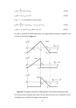
equal to the stored charge. This area can be obtained by:](https://image.slidesharecdn.com/4863057c-21bb-4299-b0f6-de43b89726de-151001054941-lva1-app6892/85/FINAL-REPORT-62-320.jpg)
![51
[ ]
[ ]
If these equations are solved for , the zero crossing points can then be
determined. The bottom length of this triangle then becomes the difference between the
zero-crossing-points:
The peak capacitor current then becomes the height of the triangle:
This current occurs when the inductor current is at maximum. Using the eq.7.41 and
eq.7.42, the stored charge can then be found as:
The CCM capacitance, when , can be obtained if the charge balance principle and
the ripple voltage are applied to eq.7.43 [56] [62] [61] [64]:
7.2.1.5 The CCM Operation of Boost Converter
As mentioned before, a boost converter produces a voltage output bigger than its input. A
basic circuit of a boost converter is illustrated below in Figure 44.
Figure 44: A Boost Converter](https://image.slidesharecdn.com/4863057c-21bb-4299-b0f6-de43b89726de-151001054941-lva1-app6892/85/FINAL-REPORT-63-320.jpg)

![53
Hence the ratio of output to input voltages, which is the transfer function of the circuit, can
be expressed in terms of duty ratio:
According to the eq.7.46, it can be theoretically said that the output voltage can be
limitless. However, the physical properties of the components put a limit on the output
while implementation [56] [62] [61] [64].
7.2.1.6 Inductance in CCM Operation
When SW1 is off and SW2 is on in Figure 45, the inductor of the boost converter is load-
connected. If the load-connected duty ratio defined as in eq.7.18 is
substituted into eq.7.45 and eq.7.46 into eq.7.24, the CCM inductor becomes [64]:
The inductance in CCM operation of a converter must be the biggest value under changing
circuit conditions. Maximising the resistance will provide the biggest inductance but
minimising the duty ratio will not provide this inductance for a boost converter as it does in
a buck converter. This can be observed by differentiating eq.7.47 with respect to the duty
ratio and setting the resulting expression to zero [61]:
{
The duty ratio of 1 is not practically preferable and it does not give the maximum
inductance. Hence, the maximum inductance can be obtained by the duty ratio of 1/3 [56].](https://image.slidesharecdn.com/4863057c-21bb-4299-b0f6-de43b89726de-151001054941-lva1-app6892/85/FINAL-REPORT-65-320.jpg)
![54
7.2.2 Discontinuous Conduction Mode (DCM)
The voltage and current waveforms of a converter in DCM operation are shown in Figure
47. The zero average principle indicates that the average voltage across the inductance is
equal to zero. If this is applied to the voltage waveform of the inductor gives the time when
the current becomes zero. This is called the extinction time [56]:
( )
Figure 47: Inductor voltage and current of the converter on DCM operation
7.2.2.1 Discontinuous Conduction Mode (DCM) Duty Ratio
The load current described in eq.7.23 shows that the relationship between the average
inductor current and the load current depends on the duty ratio and the load connected duty
ratio. This provides that a general expression can be derived for the DCM duty ratio. The
average inductor current on DCM can be calculated by area under the current wave form
given in Figure 47. The maximum inductor current is the height of the triangle defined as:](https://image.slidesharecdn.com/4863057c-21bb-4299-b0f6-de43b89726de-151001054941-lva1-app6892/85/FINAL-REPORT-66-320.jpg)
![55
Since the base of the triangle gives the extinction time, the average inductor current on
DCM then becomes [56]:
( )
The output current can be obtained by multiplying the average inductor current by the load
connected duty ratio:
( )
Hence the DCM duty ratio becomes:
√
7.2.2.2 Discontinuous Conduction Mode (DCM) Lambda Ratio and Inductance
The lambda ratio is the ratio of the circuit inductance to the CCM inductance [56]:
The duty ratio in eq.7.54 is also the CCM duty ratio as the -ratio is based on the CCM
inductance:
Then the solution of eq.7.55 gives L:
7.2.2.3 DCM Duty Ratio by Lambda Ratio
In order to obtain the DCM duty ratio in terms of lambda ratio, eq.7.56 is substituted into
eq.7.53:
√](https://image.slidesharecdn.com/4863057c-21bb-4299-b0f6-de43b89726de-151001054941-lva1-app6892/85/FINAL-REPORT-67-320.jpg)
![56
Eq.7.57 shows that there is a relationship between the CCM duty ratio and the DCM duty
ratio through the lambda ratio:
√
This indicates that the DCM ratio can be obtained when the CCM duty ratio is known [56].
7.2.2.4 Capacitance in Discontinuous Conduction Mode
The capacitor current in the converter is obtained when the load current is subtracted from
the inductor current. The load current is supplied by the capacitor current when the
inductor current is zero where the inductor is disconnected from the load. The DCM
inductor current during on time when the minimum current is zero [56]:
And during the off time:
Finally, during from the extinction time to the end of period:
The capacitor current becomes the inductor current minus the load current when the load
connected duty ratio is unity.
If , the capacitor current is then:
The capacitor supplies the load current from until the end of the period when the
inductor is load connected.
If , the capacitor current is then:](https://image.slidesharecdn.com/4863057c-21bb-4299-b0f6-de43b89726de-151001054941-lva1-app6892/85/FINAL-REPORT-68-320.jpg)
![59
√
The charge in the capacitor can be calculated when eq.7.76 and 7.71 are substituted into
eq.7.68:
( √ )
Then the ripple definition and eq.7.77 results in the DCM capacitor when there is a unity
load connected duty ratio:
( √ )
If and the substitution of the term into eq.7.70 gives the DCM inductance if the
load connected duty ratio is equal to on-time:
√
The charge in the capacitor from Figure 48:
Eq.7.72 and 7.79 together yields for zero crossing point in terms of lambda ratio as:
√
Eq.7.79 and 7.72 together yields for the peak capacitor current [62]:
(
√
)
If eq.7.81 and 7.82 are substituted into eq.7.80, the charge in the capacitor is then [61]:
( √ )
√](https://image.slidesharecdn.com/4863057c-21bb-4299-b0f6-de43b89726de-151001054941-lva1-app6892/85/FINAL-REPORT-71-320.jpg)
![60
Then finally the DCM capacitance with the ripple voltage for a load connected duty ratio
of D:
( √ )
√
If and the substitution of the term into eq.7.70 gives a DCM inductance:
√
The peak capacitor current is obtained by substituting eq.7.85 into eq.7.69:
*
√
+
The charge is the area above the time-axis in Figure 48:
The base of triangle [56]:
Then the triangle base in terms of lambda ratio by substituting eq.7.85 and 7.86 into7.88:
√ √
The charge in the capacitor is then [57]:
√ √
√
[ √ ]
Then finally the DCM capacitance for a load connected duty ratio of and
with the definition of ripple [59]:
√ √
√
[ √ ]](https://image.slidesharecdn.com/4863057c-21bb-4299-b0f6-de43b89726de-151001054941-lva1-app6892/85/FINAL-REPORT-72-320.jpg)
![61
7.2.2.5 The DCM Operation of Boost Converter
The duty ration on DCM operation is obtained by eq.7.45 and 7.57:
√
Hence the output voltage [64]:
√
Then the transfer function of the converter [56]:
√
All the above calculations and derivations show that the converter requires a considerable
amount of background knowledge and considerations in terms of a better operation [59].
7.3 Simulation of DC-DC Boost Converter Using
Matlab&Simulink
An unregulated voltage is supplied by a PV module which fluctuates during its operation
because of the effects of both temperature and radiation as discussed before in section
Error! Reference source not found.. DC-DC converters have been broadly used in many
ower systems applications such as switch mode DC power suppliers. Use of converters has
also become significantly important for renewable energy generation. PV applications in
particular use a considerable number of different converter topologies. These converters
regulate the average output voltage to a desired value despite the fact that the input voltage
value varies. This regulation is achieved by the absorption of the energy from the source
and the injection into the load. These two processes are controlled by relative time
intervals provided by the switching cycle. As defined in section 7.2, the converter can run
in two modes depending on the energy storage and the switching period. If the length of
the switching period is too much or the energy storage capacity is too small, the stored
energy is transmitted to the load before the beginning of the next cycle [65] [66].](https://image.slidesharecdn.com/4863057c-21bb-4299-b0f6-de43b89726de-151001054941-lva1-app6892/85/FINAL-REPORT-73-320.jpg)
![62
For the purpose of the simulation, several methods can be used to model the dc-dc boost
converter such as averaged models using state space equations or using the provided circuit
components in Simulink environment.
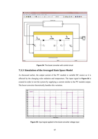
7.3.1 State Space Averaging of a Boost Converter
Considering the boost converter circuit given in Figure 49, the state variables are the
inductor current and the capacitor voltage [67].
Figure 49: An illustration dc-dc boost converter with related currents
Hence the state vector can be expressed as :
| |
In the further steps of the modelling, the conduction loss occurring on the transistor will be
showed as a resistor and denoted as . The voltage drop across the diode will be denoted
as [68].
The input vector contains the input voltage and the diode voltage . Hence the
input vector is expressed as [69]:
| |
The input current needs to be found in order to model the input of the converter. The
output vector ought to include the input current for its calculation. Hence the output vector
is expressed as:
| |](https://image.slidesharecdn.com/4863057c-21bb-4299-b0f6-de43b89726de-151001054941-lva1-app6892/85/FINAL-REPORT-74-320.jpg)
![63
It should be noted that the output voltage is not necessarily included in the output
vector as the state vector already includes it. The interest is to find the state
equations that represent the converter system. The form of the state equation is:
Here represents a matrix which includes the inductance, capacitance and mutual
inductance values and the matrices A, B, C, D includes the proportionality constants [70].
Depending on the position of the switching element in the circuit, the state equations can
be derived. For the on position of the transistor, the circuit in Figure 50 is obtained:
Figure 50: Converter circuit when the transistor is on position
In this position, the inductor current, source current, and capacitor current are derived as:
If these equations are represented in the state space form:
* + [ ] [ ] [ ] * + [ ]](https://image.slidesharecdn.com/4863057c-21bb-4299-b0f6-de43b89726de-151001054941-lva1-app6892/85/FINAL-REPORT-75-320.jpg)
![64
The output matrices are:
[ ][ ] [ ][ ]
For the off position of the transistor, the circuit in Figure 51 is obtained:
Figure 51: Converter circuit when the transistor is off position
In this position, the inductor current, source current, and capacitor current are derived as:
If these equations are represented in the state space form [71]:
* + [ ] [ ] [ ] * + [ ]
The output matrices are:
[ ][ ] [ ][ ]
These equations can be represented in a single state space model by adding the switch
position into the system. The converter contains continuous and discrete signals. The](https://image.slidesharecdn.com/4863057c-21bb-4299-b0f6-de43b89726de-151001054941-lva1-app6892/85/FINAL-REPORT-76-320.jpg)
![65
inductor current, capacitor current, input and output voltages are continuous whereas the
switching signal is a discrete signal which shows the position of the switch. The combined
state space equations are then:
[ ]
[ ]
Hence the state space model with the assumption that the source voltage is constant is:
[ ] [ ] [ ] [ ]
7.3.2 Implementation of Averaged State Space Model
The averaged model in eq.7.111 can then be implemented in Simulink environment by
using the mathematical blocks:
Figure 52: Simulink implementation of dc-dc boost converter](https://image.slidesharecdn.com/4863057c-21bb-4299-b0f6-de43b89726de-151001054941-lva1-app6892/85/FINAL-REPORT-77-320.jpg)


![70
Chapter 8
8 The Implementation of MPPT Algorithm
As expressed earlier in section 4, there have been many developments in the PV MPPT
systems since the need for the maximum power extraction from the PV system has been
significantly important. If considered that there is a huge investment on a PV power
generation system, it is essential to obtain the maximum benefit and profit out of the
investment to make it feasible and viable in the end.
The photovoltaic power generation is not similar to the conventional systems which use
water or steam turbines where a smooth and suitable power for the conventional grid can
be supplied. There might be huge power losses when the changing distinctive characteristic
of photovoltaic systems cannot be handled appropriately.
Among the algorithms that have been expressed in section 4, Perturb & Observe algorithm
has advantages such as being easy and cheap for the implementation.
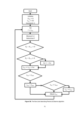
8.1 Perturb & Observe MPPT Algorithm
Mainly, perturb and observe maximum power point tracking algorithm drives the PV
system to the direction where the output power increases. The change of power is
calculated by subtracting the previous measured value from the new measured value. If the
resulting value is positive, the direction of the incremental current will be kept the same,
and if it is negative, the direction will be changed in the opposite way.
The flow chart related to the P & O algorithm is given in Figure 58 [72]. In order to
implement the algorithm in Simulink environment, the developed programming language
of Matlab needs to be understood. The software is similar to the C++ and Fortran computer
languages, which is actually a mixture of both languages.
The implementation of the algorithm combined with the modelled dc-dc boost converter
and the PV module earlier in sections 6 and 7 is represented in Appendix 2. The obtained
results are represented in the following section.](https://image.slidesharecdn.com/4863057c-21bb-4299-b0f6-de43b89726de-151001054941-lva1-app6892/85/FINAL-REPORT-82-320.jpg)


![77
11 References
[1] Snyman, D.B.; Enslin, J.H.R., "Simplified maximum power point controller for PV installations."
Photovoltaic Specialists Conference, 1993., Conference Record of the Twenty Third IEEE,
Stellenbosch Univ. : IEEE, 06 August 2002, pp. 1240-1245. Print ISBN: 0-7803-1220-1.
[2] Safari A. Mekhilef S., "Simulation and Hardware Implementation of Incremental Conductance
MPPT with Direct Control Method Using Cuk Converter." Industrial Electronics, IEEE Transactions ,
Kuala Lumpur, Malaysia : IEEE, 10 March 2011, Issue 4, Vol. 58, pp. 1154-1161. ISSN : 0278-0046 .
[3] Chiu, Chian-Song., "T-S Fuzzy Maximum Power Point Tracking Control of Solar Power
Generation Systams." Energy Conversion, IEEE Transactions, Jhongli, Taiwan : IEEE, 18 November
2010, Issue 4, Vol. 25, pp. 1123-1132. ISSN : 0885-8969.
[4] Koutroulis, E.; Kalaitzakis, K.; Voulgaris, N.C.;., "Development of a microcontroller-based,
photovoltaic maximum power point tracking control system." Power Electronics, IEEE
Transactions, Univ. of Crete, Chania : IEEE, 07 August 2002, Issue 1, Vol. 16, pp. 46-54. ISSN : 0885-
8993.
[5] Noguchi, T.; Togashi, S.; Nakamoto, R.;., "Short-current pulse based adaptive maximum-power-
point tracking for photovoltaic power generation system." Industrial Electronics, 2000. ISIE 2000.
Proceedings of the 2000 IEEE International Symposium, Univ. of Technol., Niigata : IEEE, 06 August
2002, Vol. 1, pp. 157-162. Print ISBN: 0-7803-6606-9 .
[6] Liu Chun-xia; Liu Li-qun;., "An improved perturbation and observation MPPT method of
photovoltaic generate system." Industrial Electronics and Applications, 2009. ICIEA 2009. 4th IEEE
Conference, Taiyuan, China : IEEE, 30 June 2009, pp. 2966-2970. Print ISBN: 978-1-4244-2799-4 .
[7] Mary D. Archer, Robert Hill., Clean Electricity From Photovoltaics. London : Imperial College
Press, 2001. 1-86094-161-3.
[8] Wang NianCHun; Sun Zuo; Yukita, K.; Goto, Y.; Ichiyanagi, K.;., "Research of PV Model and
MPPT Methods in Matlab." Power and Energy Engineering Conference (APPEEC), 2010 Asia-Pacific
, Nanjing, China : IEEE, 15 April 2010, pp. 1-4. Print ISBN: 978-1-4244-4812-8 .
[9] Kadri, R.; Gaubert, J.-P.; Champenois, G.;., "An Improved Maximum Power Point Tracking for
Photovoltaic Grid-Connected Inverter Based on Voltage-Oriented Control." Industrial Electronics,
IEEE Transactions, Poitiers, France : IEEE, 10 December 2010, Issue 1, Vol. 58, pp. 66-75. ISSN :
0278-0046 .
[10] Vanden Eynde, N.W.; Chowdhury, S.; Chowdhury, S.P.; ., "Modeling and simulation of a
stand-alone photovoltaic plant with MPPT feature and dedicated battery storage." Power and
Energy Society General Meeting, 2010 IEEE , Cape Town, South Africa : IEEE, 30 Septemner 2010,
pp. 1-8. ISSN : 1944-9925 E-ISBN : 978-1-4244-8357-0 Print ISBN: 978-1-4244-6549-1 .
[11] Ramesh Oruganti, Ted Spooner & Faz Rahman., "TECHNOLOGICAL CHALLENGES AND
OPPORTUNITIES IN PHOTOVOLTAIC ENERGY SYSTEMS ." Singapore , Australia : s.n.](https://image.slidesharecdn.com/4863057c-21bb-4299-b0f6-de43b89726de-151001054941-lva1-app6892/85/FINAL-REPORT-89-320.jpg)
![78
[12] Petrone, G.; Spagnuolo, G.; Teodorescu, R.; Veerachary, M.; Vitelli, M.; ., "Reliability Issues in
Photovoltaic Power Processing Systems." Industrial Electronics, IEEE Transactions, Univ. di
Salerno, Fisciano : IEEE, 24 June 2008, Issue 7, Vol. 55, pp. 2569 - 2580. ISSN: 0278-0046 .
[13] Markvart, Tomas., Solar Electricity. Chicester : John Wiley & Sons Ltd, 1994. ISBN 0-471-
94161-1.
[14] , Esdal College. [Online] [Cited: 12 08 2011.]
http://www.esdalcollege.nl/eos/vakken/na/zonnecel.htm.
[15] Weiping Luo, Gijing Han., "The Algorithms Research of Maximum Power Point Tracking in
Grid-Connected Photovoltaic Generation System." Knowledge Acquisition and Modeling, 2009.
KAM '09. Second International Symposium, Wuhan, China : IEEE, 28 December 2009, Vol. 2, pp.
77-80. Print ISBN: 978-0-7695-3888-4 .
[16] Jiyong Li, Hanghua Wang., "Maximum Power Point Tracking of Photovoltaic Generation Based
on the Fuzzy Control Method." Sustainable Power Generation and Supply, 2009. SUPERGEN '09.
International Conference, Nanjing, China : IEEE, 04 December 2009, pp. 1-6. Print ISBN: 978-1-
4244-4934-7 .
[17] M. Berrera, A. Dolara, Student Member, IEEE, R. Faranda, Member, IEEE,and S. Leva,
Member, IEEE., "Experimental test of seven widely-adopted MPPT algorithms." PowerTech, 2009
IEEE Bucharest , Milan, Italy : IEEE, 09 October 09, pp. 1-8. Print ISBN: 978-1-4244-2234-0.
[18] Roberto Franda, Sonia Leva., "Energy comparison of MPPT techniques for PV Systems."
WSEAS TRANSACTIONS on POWER SYSTEMS, Milano, Italy : WSEAS .
[19] Ahmad Al-Diab, Constantinos Sourkounis., "Variable Step Size P&O MPPT Algorithm for PV
Systems." Optimization of Electrical and Electronic Equipment (OPTIM), 2010 12th International
Conference, Bochum, Germany : IEEE, 15 July 2010, pp. 1097-1102. ISSN: 1842-0133 Print ISBN:
978-1-4244-7019-8.
[20] Trishan Esram, Student Member Patrick L. Chapman, Member., "Comparison of Photovoltaic
Array Maximum Power Point Tracking Techniques." Energy Conversion, IEEE Transactions,
Urbana, IL : IEEE, 21 May 2007, Issue 2, Vol. 22, pp. 439-449. ISSN : 0885-8969 .
[21] A. DOLARA, R. FARANDA, S. LEVA., "Energy Comparison of Seven MPPT Techniques for PV
Systems." Journal of Electromagnetic Analysis and Applications , Milano, Italy : Scientific Research,
September 2009, Issue 3, Vol. 1, pp. 152-162. ISSN Print: 1942-0730 ISSN Online: 1942-0749 .
[22] NAZIH MOUBAYED, ALI EL-ALI, RACHID OUTBIB,., "Comparison of Two MPPT Techniques for
PV System." WSEAS TRANSACTIONS on ENVIRONMENT and DEVELOPMENT, Tripoli, LEBANON.
Marseille, FRANCE. : s.n., December 2009, Issue 12, Vol. 5. ISSN: 1790-5079.
[23] Wu-Shun Jwo, Chia-Chang Tong, IEEE member, Chi-Jui Chao., "FIRMWARE IMPLEMENTATION
OF AN ADAPTIVE SOLAR CELL MAXIMUM POWER POINT TRACKING BASED ON PSoC." Photovoltaic
Specialists Conference (PVSC), 2010 35th IEEE, Changhua, Taiwan : IEEE, 01 November 2010, pp.
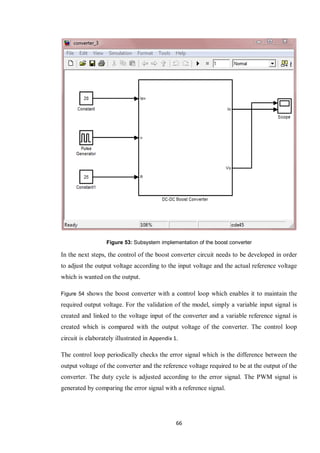
407-411. ISSN : 0160-8371 Print ISBN: 978-1-4244-5890-5 .](https://image.slidesharecdn.com/4863057c-21bb-4299-b0f6-de43b89726de-151001054941-lva1-app6892/85/FINAL-REPORT-90-320.jpg)
![79
[24] Hardik P. Desai, and H. K. Patel,., "Maximum Power Point Algorithm in PV Generation: An
Overview." Power Electronics and Drive Systems, 2007. PEDS '07. 7th International Conference,
Surat, India : IEEE, 11 Aril 2008, pp. 624-630. Print ISBN: 978-1-4244-0645-6 .
[25] D. P. Hohm, M. E. Ropp., "Comparative Study of Maximum Power Point Tracking Algorithms
Using an Experimental, Programmable, Maximum Power Point Tracking Test Bed." Photovoltaic
Specialists Conference, 2000. Conference Record of the Twenty-Eighth IEEE , South Dakota State
University : IEEE, 06 August 2002, pp. 1699 - 1702. Print ISBN: 0-7803-5772-8 .
[26] Barna Szabados, Fangnan Wu., "A Maximum Power Point Tracker Control of A Photovoltaic
System." Instrumentation and Measurement Technology Conference Proceedings, 2008. IMTC
2008. IEEE , Hamilton, ONT, Can. : IEEE, 12-15 May 2008, pp. 1074 - 1079 . ISSN : 1091-5281 Print
ISBN: 978-1-4244-1540-3 .
[27] Guohui Zeng, Qizhong Liu., "An Intelligent Fuzzy Method for MPPT of Photovoltaic arrays."
Computational Intelligence and Design, 2009. ISCID '09. Second International Symposium ,
Shanghai, P. R. China : Second International Symposium on Computational Intelligence and
Design, 12-14 December 2009, Vol. 2, pp. 356 - 359. Print ISBN: 978-0-7695-3865-5 .
[28] Xiao-bo Li, Ke Dong, Hao Wu., "Study on the Intelligent Fuzzy Control Method for MPPT in
Photovoltaic Voltage Grid System." Industrial Electronics and Applications, 2008. ICIEA 2008. 3rd
IEEE Conference, Qingdao : IEEE, 01 August 2008, pp. 708-711. Print ISBN: 978-1-4244-1717-9 .
[29] F.Bouchafaa, D.Beriber, M.S.Boucherit., "Modeling and simulation of a gird connected PV
generation system With MPPT fuzzy logic control." Systems Signals and Devices (SSD), 2010 7th
International Multi-Conference, Algiers, Algeria : IEEE, 27 September 2010, pp. 1-7. Print ISBN:
978-1-4244-7532-2 .
[30] XIE Wei, HUI Jing., "MPPT for PV System Based on A Novel Fuzzy Control Strategy." Digital
Manufacturing and Automation (ICDMA), 2010 International Conference , Wuxi, Jiangsu, China :
IEEE, 24 January 2011, Vol. 1, pp. 960-963. Print ISBN: 978-0-7695-4286-7.
[31] K. Samangkool and S. Premrudeepreechacharn., "Maximum Power Point Tracking Using
Neural Networks for Grid-Connected Photovoltaic System." Future Power Systems, 2005
International Conference, Thailand : IEEE, 06 March 2006, pp. 4 pp.- 4. Print ISBN: 90-78205-02-4 .
[32] R.Ramaprabha, Member, IEEE, B.L.Mathur and M.Sharanya., "Solar Array Modeling and
Simulation of MPPT using Neural Network." Control, Automation, Communication and Energy
Conservation, 2009. INCACEC 2009. 2009 International Conference , Chennai, India : IEEE, 18
August 2009, pp. 1-5. Print ISBN: 978-1-4244-4789-3.
[33] Jonathan W. Kimball, Senior Member, Philip T. Krein, Fellow., "Digital Ripple Correlation
Control for Photovoltaic Applications." Power Electronics Specialists Conference, 2007. PESC 2007.
IEEE, Champaign, IL 61820, Urbana, IL 61801 : IEEE, 17-21 June 2007, pp. 1690-1694. ISSN: 0275-
9306 Print ISBN: 978-1-4244-0654-8 .](https://image.slidesharecdn.com/4863057c-21bb-4299-b0f6-de43b89726de-151001054941-lva1-app6892/85/FINAL-REPORT-91-320.jpg)
![80
[34] Jonathan W. Kimball and Philip T. Krein., "Discrete-Time Ripple Correlation Control for
Maximum Power Point Tracking." Power Electronics, IEEE Transactions , Rolla, MO : IEEE, 25
November 2008, Issue 5, Vol. 23, pp. 2353-2362. ISSN : 0885-8993 .
[35] Trishan Esram, Student Member, IEEE, Jonathan W. Kimball, Senior Member, IEEE, Philip T.
Krein, Fellow, IEEE,Patrick L. Chapman, Senior Member, IEEE, and Pallab Midya, Senior Member,
IEEE., "Dynamic Maximum Power Point Tracking of Photovoltaic Arrays Using Ripple Correlation
Control." Power Electronics, IEEE Transactions, Illinois Univ., Urbana, IL : IEEE, 06 September 2006,
Issue 5, Vol. 21, pp. 1282-1291. ISSN : 0885-8993.
[36] G. Spiazzi, S. Buso, P. Mattavelli and P. Tenti., "Low complexity MPPT techniques for PV
module converters." Power Electronics Conference (IPEC), 2010 International , Padova, Italy :
IEEE, 09 August 2010, pp. 2074-2081. Print ISBN: 978-1-4244-5394-8 .
[37] Veysel T. Buyukdegirmenci, Ali M. Bazzi, and Philip T. Krein., "A Comparative Study of an
Exponential Adaptive Perturb and Observe Algorithm and Ripple Correlation Control for Real-Time
Optimization." Control and Modeling for Power Electronics (COMPEL), 2010 IEEE 12th Workshop,
Urbana-Champaign, Urbana, IL, USA : IEEE, 28-30 June 2010. E-ISBN: 978-1-4244-7461-5 Print
ISBN: 978-1-4244-7462-2 .
[38] Armando Bellini, Stefano Bifaretti, Vincenzo Iacovone., "MPPT Algorithm for Current
Balancing of Partially Shaded Photovoltaic Modules." Industrial Electronics (ISIE), 2010 IEEE
International Symposium, Rome, Italy : IEEE, 15 November 2010, pp. 933-938. Print ISBN: 978-1-
4244-6390-9 .
[39] Vanxay Phimmasone, Tsugio Endo, Yuta Kondo and Masafumi Miyatake., "Improvement of
the Maximum Power Point Tracker for Photovoltaic Generators with Particle Swarm Optimization
Technique by Adding Repulsive Force among Agents." Electrical Machines and Systems, 2009.
ICEMS 2009. International Conference, Tokyo Japan : IEEE, 15 January 2010, pp. 1-6. Print ISBN:
978-1-4244-5177-7 .
[40] Kenji Kobayashi, Ichiro Takano and Yoshio Sawada., "A Study on a Two Stage Maximum
Power Point Tracking Control of a Photovoltaic System under Partially Shaded Insolation
Conditions." Power Engineering Society General Meeting, 2003, IEEE, Tokyo, Japan : IEEE, 13-17
July 2003, Vols. 4 - 2617 Vol. 4 . Print ISBN: 0-7803-7989-6 .
[41] Young-Hyok Ji, Doo-Yong Jung, Jun-Gu Kim, Jae-Hyung Kim, Tae-Won Lee, Chung-Yuen Won.,
"A Real Maximum Power Point Tracking Method for Mismatching Compensation in PV Array
under Partially Shaded Conditions." Power Electronics, IEEE Transactions, Suwon, South Korea :
IEEE, 21 October 2010, Issue 4, Vol. 26, pp. 1001 - 1009. ISSN : 0885-8993.
[42] Marcelo Gradella Villalva, Jonas Rafael Gazoli, Ernesto Ruppert Filho., "MODELING AND
CIRCUIT-BASED SIMULATION OF PHOTOVOLTAIC ARRAYS." Power Electronics Conference, 2009.
COBEP '09. Brazilian, University of Campinas (UNICAMP), Brazil : IEEE, 04 December 2009, pp.
1244 - 1254. Print ISBN: 978-1-4244-3369-8 ISSN : 2175-8603.
[43] V. Di Dio, D. La Cascia, R. Miceli, C. Rando., "A Mathematical Model to Determine the
Electrical Energy Production in Photovoltaic Fields Under Mismatch Effect." Clean Electrical](https://image.slidesharecdn.com/4863057c-21bb-4299-b0f6-de43b89726de-151001054941-lva1-app6892/85/FINAL-REPORT-92-320.jpg)
![81
Power, 2009 International Conference, Palermo, Italy : IEEE, 9-11 June 2009. Print ISBN: 978-1-
4244-2543-3 .
[44] Anca D. Hansen, Poul Sorensen, Lars H. Hansen, Henrik Bindner., "Models for a Standalone PV
System." Riso National Laboratory, Roskilde : Danka Services International A/S, 2001, December
2000. ISBN 87-550-2774-1.
[45] C. Carrero, J. Rodrı´guez, D. Ramı´rez, C. Platero., "Simple estimation of PV modules loss
resistances for low error modelling." Renewable Energy, Madrid : ScienceDirect, 24 November
2009, Issue 5, Vol. 35, pp. 1103-1108. ISSN 0960-1481.
[46] A. Elkholy, F. H. Fahmy, A. Abu Elela., "A New Technique for Photovoltaic Module
Performance Mathematical Model." 2010 International Conference on Chemistry and Chemical
Engineering (ICCCE 2010), Cairo, Egypt : IEEE, 1-3 August 2010, pp. 6-10. Print ISBN: 978-1-4244-
7765-4 .
[47] Jan Leuchter, Vladimir Rerucha, Ahmed F. Zobaa., "Mathematical Modeling of Photovoltaic
Systems." Power Electronics and Motion Control Conference (EPE/PEMC), 2010 14th International
, Brno, Czech Republic : IEEE, 21 October 2010, pp. S4-1 - S4-4 . Print ISBN: 978-1-4244-7856-9.
[48] Marcelo Gradella Villalva, Jonas Rafael Gazoli, and Ernesto Ruppert Filho., "Comprehensive
Approach to Modeling and Simulation of Photovoltaic Arrays." Power Electronics, IEEE
Transactions, Univ. of Campinas, Campinas : IEEE, Power Electronics, 17 April 2009, Issue 5, Vol.
24, pp. 1198 - 1208. ISSN: 0885-8993 .
[49] Krenzinger A, Wagner LA., "Computer Simulation of Stand Alone PV Systems for Developing
Countries." 11th European PV Solar Energy Conference, Montreaux, Switzerland : IEEE, 1992.
[50] Tsai, Huan-Liang., "Insolation-oriented model of photovoltaic module using
Matlab/Simulink." Solar Energy, Chang-Hua, Taiwan : ScienceDirect, 14 May 2010, Issue 7, Vol. 84,
pp. 1318-1326. ISSN 0038-092X.
[51] Soto, Widalys De., Improvement and Validation of a Model for Photovoltaic Array
Performance. Mechanical Engineering. Madison : University of Wisconsin, 2004. Master of Science
Thesis.
[52] Nejib Hamrouni , Moncef Jraidi, Adne`ne Che´rif., "Theoretical and experimental analysis of
the behaviour of a photovoltaic pumping system." Solar Energy, Belvedere, Tunis, Tunisia :
ScienceDirect, 5 April 2009, Issue 8, Vol. 83, pp. 1335-1344. ISSN 0038-092X.
[53] E. Skoplaki, J.A. Palyvos., "Operating temperature of photovoltaic modules:A survey of
pertinent correlation s." Renewable Energy, Athens 15780, Greece : Elsevier, 24 June 2008, Issue
1, Vol. 34, pp. 23-29. ISSN 0960-1481.
[54] Mayo-Maldonado, J.C. ; Salas-Cabrera, R. ; Rosas-Caro, J.C. ; De Leon-Morales, J. ; Salas-
Cabrera, E.N. ;., "Modelling and control of a DC-DC multilevel boost converter." Power Electronics,
IET, Madero City Technol. Inst., Madero, Mexico : IEEE, 27 June 2011, Issue 6, Vol. 4, pp. 693 - 700
. ISSN : 1755-4535 .](https://image.slidesharecdn.com/4863057c-21bb-4299-b0f6-de43b89726de-151001054941-lva1-app6892/85/FINAL-REPORT-93-320.jpg)
![82
[55] Siwakoti, Yam Prasad, Bhupendra Bimal Chhetri, Brijesh Adhikary, Diwakar Bista.,
"MICROCONTROLLER BASED INTELLIGENT DC/DC CONVERTER TO TRACK MAXIMUM POWER
POINT OR SOLAR PHOTOVOLTAIC MODULE." Innovative Technologies for an Efficient and Reliable
Electricity Supply (CITRES), 2010 IEEE Conferenc, Kathmandu University, Nepal : IEEE, 04
November 2010, pp. 94-101. Print ISBN: 978-1-4244-6076-2 .
[56] Shaffer, Randall., Fundamentals of Power Electronics with Matlab. 1st. Boston : CHARLES
RIVER MEDIA , 2007. ISBN 1-58450-852-3.
[57] Stiebler, Prof. Dr. Manfred., Wind Energy Systems for Electric Power Generation. Berlin :
Springer-Verlag Berlin Heidelberg, 2008. ISBN: 978-3-540-68762-7 .
[58] Mukund R. Patel, Ph.D., P.E., Wind and Solar Power Systems. Kings Point : CRC Press, 1999.
ISBN 0-8493-1605-7.
[59] Wu, Keng C., Switch-Mode Power Converters. London : Elsevier Academic Press, 2006. ISBN 0-
12-088795-9.
[60] KAZIMIERCZUK, MARIAN K., Pulse-width Modulated DC–DC Power Converters. Dayton : John
Wiley & Sons, Ltd, 2008. ISB N: 978-0-470-77301-7 (HB).
[61] Fewson, Denis., Introduction to Power Electronics. London : Arnold, a member of the Hodder
Headline Group, 1998. ISBN 0 340 69143 3 (pb) .
[62] , Introduction to Power Electronics. s.l. : Valery Vodovozov & Ventus Publishing ApS, 2010.
ISBN 978-87-7981-625-4.
[63] Costabeber, A.; Mattavelli, P.; Saggini, S.; Bianco, A.;., "Digital Autotuning of dc-dc Converters
Based on Model Reference Impulse Response." Power Electronics, IEEE Transactions, s.l. : IEEE, 03
March 2011, Issue 1, Vol. PP, p. 1. ISSN : 0885-8993 .
[64] Marauchos, C.C., The Switching Function. [ed.] Dr. R. S. Soin, Dr. D. G. Haigh and Professor Y.
Sun. 17. London : The Institution of Engineering and Technology, 2006. ISBN 978-0-86341-351-3.
[65] Jacobina, C.B.; dos Santos, E.C.; Rocha, N.; ., "Generalized ac-dc single-phase boost rectifier."
Applied Power Electronics Conference and Exposition (APEC), 2010 Twenty-Fifth Annual IEEE ,
Campina Grande, Brazil : IEEE, 18 March 2010, pp. 1183 - 1190 . ISSN : 1048-2334 .
[66] Yu Du; Xiaohu Zhou; Sanzhong Bai; Lukic, S.; Huang, A.; ., "Review of non-isolated bi-
directional DC-DC converters for plug-in hybrid electric vehicle charge station application at
municipal parking decks." Applied Power Electronics Conference and Exposition (APEC), 2010
Twenty-Fifth Annual IEEE , Raleigh, NC, USA : IEEE, 18 March 2010, pp. 1145 - 1151. ISSN : 1048-
2334.
[67] Nwosu, C.A., "State-Space Averaged Modeling of a Nonideal Boost Converter. ." The Pacific
Journal of Science and Technology , Nsukka, Nigeria : s.n., November 2008, Issue 2, Vol. 9.
[68] Hasaneen, B.M.; Elbaset Mohammed, A.A.; ., "DESIGN AND SIMULATION OF DC/DC BOOST
CONVERTER." Power System Conference, 2008. MEPCON 2008. 12th International Middle-East,
Kena : IEEE, 15 July 2008, pp. 335 - 340 . Print ISBN: 978-1-4244-1933-3 .](https://image.slidesharecdn.com/4863057c-21bb-4299-b0f6-de43b89726de-151001054941-lva1-app6892/85/FINAL-REPORT-94-320.jpg)
![83
[69] J.C. Mayo-Maldonado; R. Salas-Cabrera; J.C. Rosas-Caro; J. De Leon-Morales; E.N. Salas-
Cabrera., "Modelling and control of a DC – DC multilevel boost converter." Mexico : IET Power
Electronics, 19 October 2010, Issue 6, Vol. 4, pp. 693-700.
[70] Sven E. Fagerstrom; Nagy N. Bengiamin ., "Buck/Boost Converter Modeling and Simulation
for Performance Optimization ." Fresno, CA USA : s.n.
[71] R. De Keyser, J. Bonilla, IEEE Member and C. Ionescu, IEEE Student Member., "A Comparative
Study of Several Control Techniques Applied to a Boost Converter." IEEE 10th Int Conf on
Optimisation of Electrical and Electronic Equipment OPTIM, Brasov Romania : s.n., 2006, pp. 71-
78. ISBN 973-635-704-X.
[72] Pongsakor Takun, Somyot Kaitwanidvilai and Chaiyan Jettanasen ., "Maximum Power Point
Tracking using Fuzzy Logic Control for Photovoltaic Systems." Proceedings of the International
Multi Conference of Engineers and Computer Scientists 2011, Hong Konh : IMECS2011, 16-18
March 2011, Vol. II. ISSN: 2078-0966.](https://image.slidesharecdn.com/4863057c-21bb-4299-b0f6-de43b89726de-151001054941-lva1-app6892/85/FINAL-REPORT-95-320.jpg)
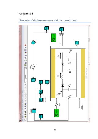


This dissertation discusses the design of a maximum power point tracker (MPPT) for photovoltaic (PV) systems. It begins with an overview of solar cell operation principles and the need for MPPT. It then reviews various common MPPT techniques including hill climbing, incremental conductance, and other methods. The dissertation also examines MPPT performance under partially shaded PV array conditions. It presents mathematical models of a PV module and DC-DC boost converter and simulations of these components in Matlab/Simulink. Finally, it implements and tests a perturb and observe MPPT algorithm in the overall system simulation.


![[Codientu.org] design of a charge controller circuit](https://cdn.slidesharecdn.com/ss_thumbnails/codientu-180501080259-thumbnail.jpg?width=640&height=640&fit=bounds)
