Downloaded 59 times
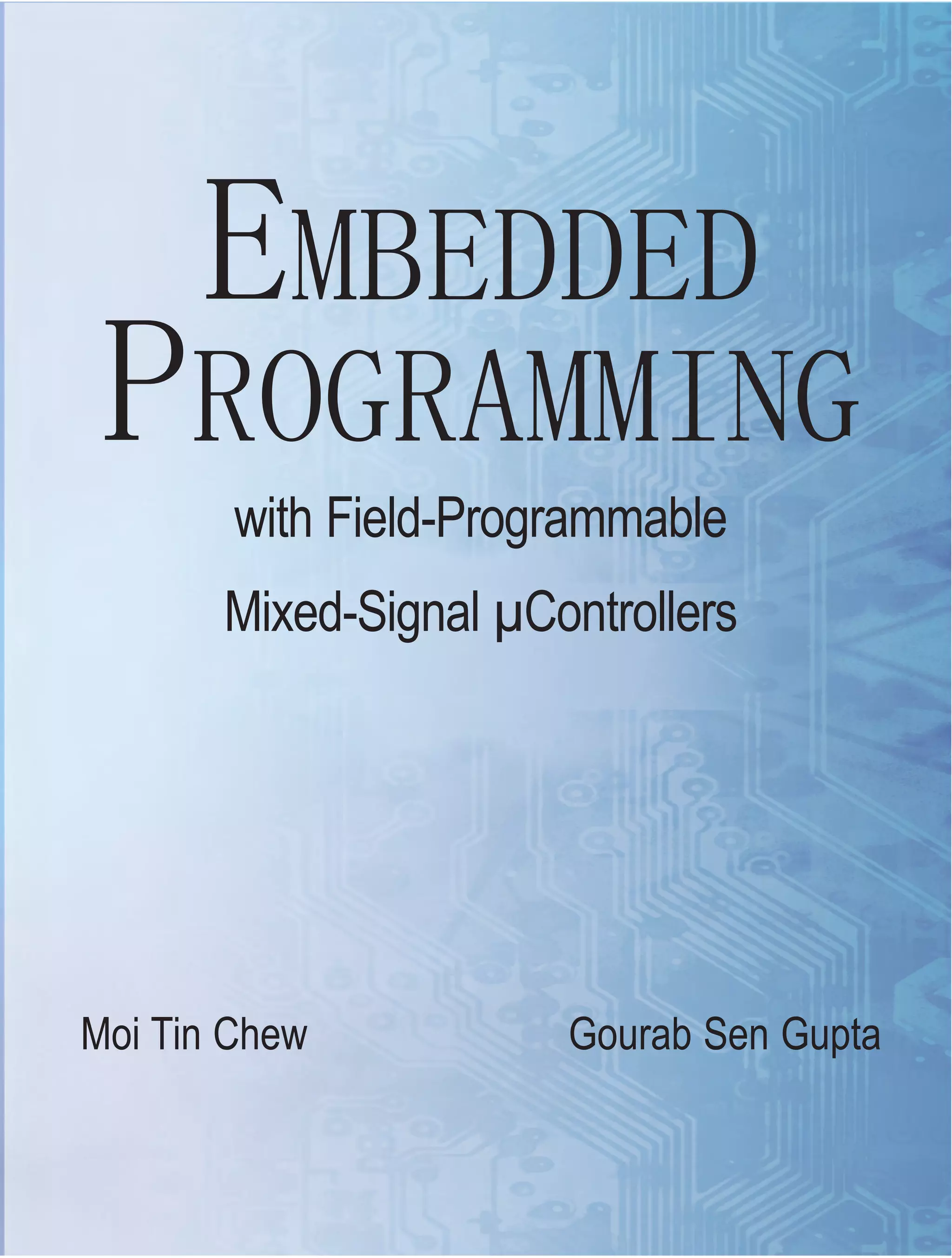


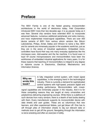
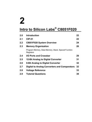
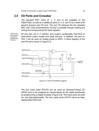
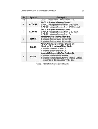
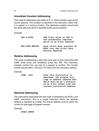
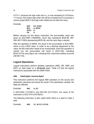
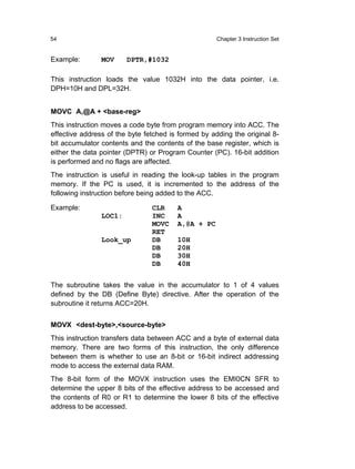
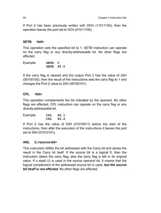
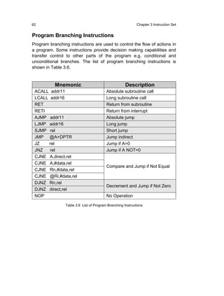
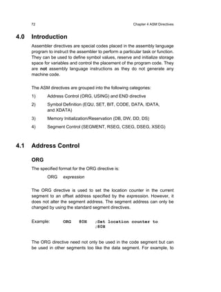
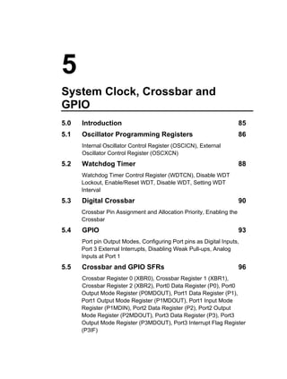
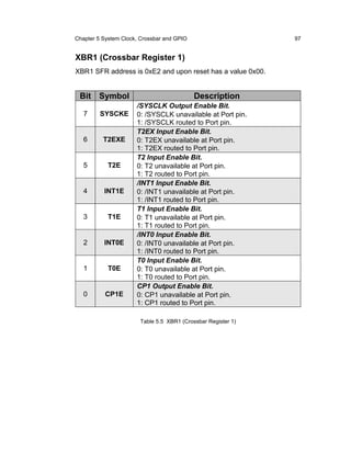
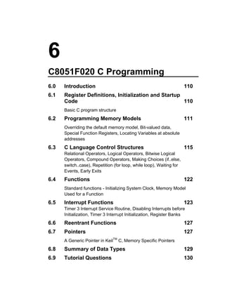
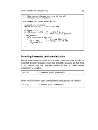
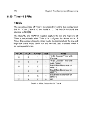
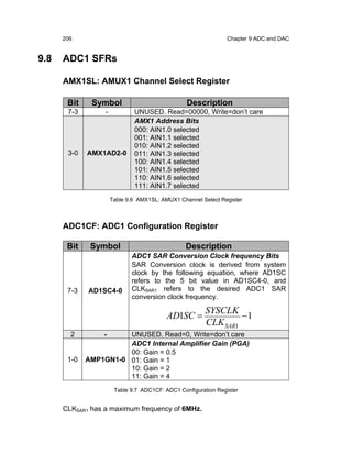
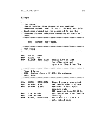
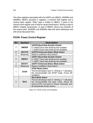
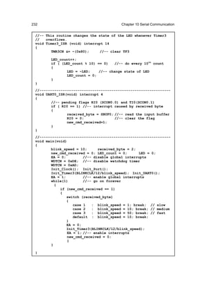
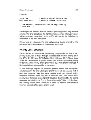
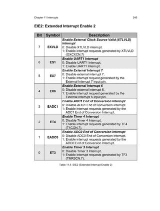
![4 Chapter 1 8051 Architecture Overview
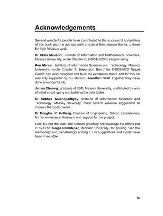
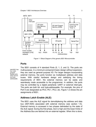
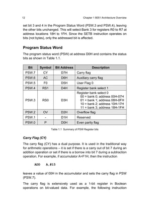
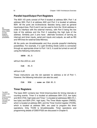
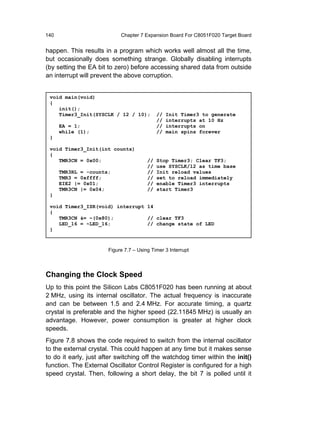
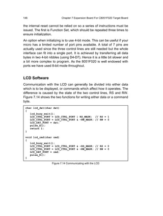
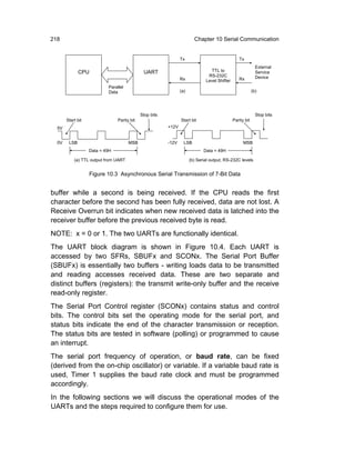
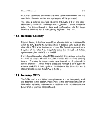
the port lines are available for data input or output. When ALE falls,
signaling the beginning of the second phase, the address latch outputs
remain fixed and are no longer dependent on the latch input. Later in the
second phase, the Data Bus controls the state of the AD[0:7] at the time
/RD or /WR is asserted.
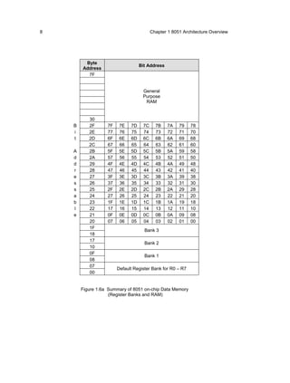
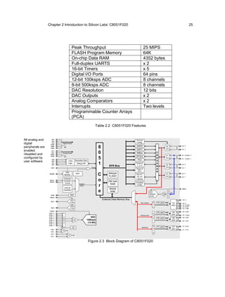
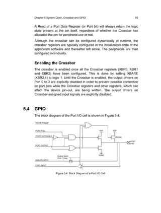
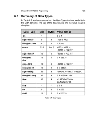
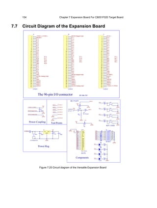
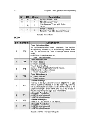
40 VCC
XTL2 18
39 P0.0 AD0
XTL1 19 38 P0.1 AD1
37 P0.2 AD2
36 P0.3 AD3
35 P0.4 AD4
34 P0.5 AD5
RXD P3.0 10 33 P0.6 AD6
TXD P3.1 11 32 P0.7 AD7
/INT0 P3.2 12
/INT1 P3.3 13 21 P2.0 AD8
T0 P3.4 14 8051 22 P2.1 AD9
T1 P3.5 15 23 P2.2 AD10
/WR P3.6 16 24 P2.3 AD11
/RD P3.7 17 25 P2.4 AD12
26 P2.5 AD13
27 P2.6 AD14
RST 9 28 P2.7 AD15
/EA 31 1 P1.0
to to
ALE 30
8 P1.7
/PSEN 29 20 VSS
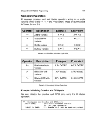
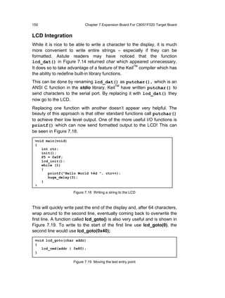
Figure 1.2 8051 pin assignment
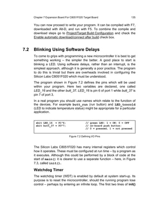
Reset (RST)
Reset circuitry allows the 8051 to be easily placed in a predefined default
condition. On entry to the reset state, the following occur:
♦ The MCU halts program execution
♦ Special Function Registers (SFRs) are initialized to their defined
reset values
♦ External port pins are forced to a known state
♦ Interrupts and timers are disabled
Sources of reset include Power-on Reset and External Reset.](https://image.slidesharecdn.com/14157565-embedded-programming-101014045310-phpapp01/85/14157565-embedded-programming-17-320.jpg)


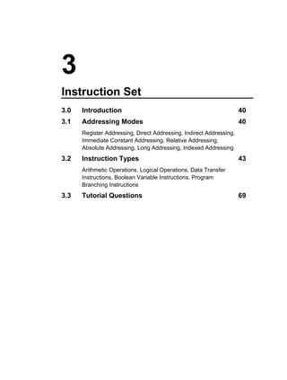
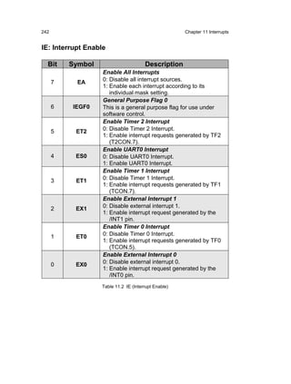
![44 Chapter 3 Instruction Set
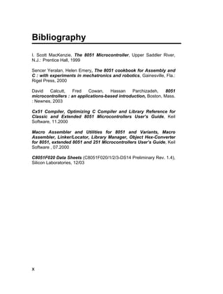
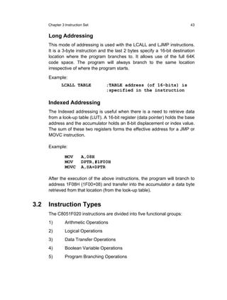
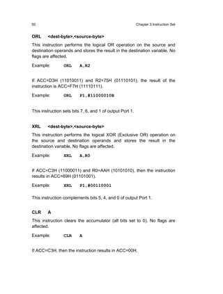
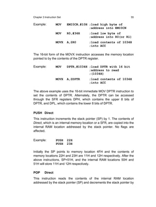
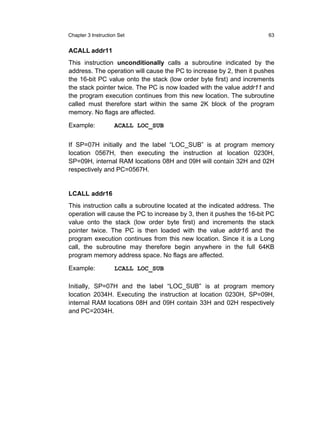
Arithmetic Operations
With arithmetic instructions, the C8051F020 CPU has no special
knowledge of the data format, e.g. signed binary, unsigned binary, binary
coded decimal, ASCII, etc. Therefore, the appropriate status bits in the
PSW are set when specific conditions are met to manage the different
data formats. Table 3.2 lists the arithmetic instructions associated with
the C8051F020 MCU.
Mnemonic Description
ADD A, Rn A = A + [Rn]
ADD A, direct A = A + [direct memory]
ADD A,@Ri A = A + [memory pointed to by Ri]
ADD A,#data A = A + immediate data
ADDC A,Rn A = A + [Rn] + CY
ADDC A, direct A = A + [direct memory] + CY
ADDC A,@Ri A = A + [memory pointed to by Ri] + CY
ADDC A,#data A = A + immediate data + CY
SUBB A,Rn A = A - [Rn] - CY
SUBB A, direct A = A - [direct memory] - CY
SUBB A,@Ri A = A - [@Ri] - CY
SUBB A,#data A = A - immediate data - CY
INC A A=A+1
INC Rn [Rn] = [Rn] + 1
INC direct [direct] = [direct] + 1
INC @Ri [@Ri] = [@Ri] + 1
DEC A A=A-1
DEC Rn [Rn] = [Rn] - 1
DEC direct [direct] = [direct] - 1
DEC @Ri [@Ri] = [@Ri] - 1
MUL AB Multiply A & B
DIV AB Divide A by B
DA A Decimal adjust A
Table 3.2 List of Arithmetic Instructions
Note: [@Ri] means contents of memory location pointed to by Ri
register](https://image.slidesharecdn.com/14157565-embedded-programming-101014045310-phpapp01/85/14157565-embedded-programming-57-320.jpg)
![Chapter 3 Instruction Set 47
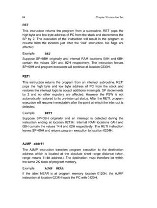
MUL AB
Multiplies A & B and the 16-bit result stored in [B15-8], [A7-0].
Multiplies the unsigned 8-bit integers in the accumulator and the B
register. The Low order byte of the 16-bit product will go to the
accumulator and the High order byte will go to the B register. If the
product is greater than 255 (FFH), the overflow flag is set; otherwise it is
cleared. The carry flag is always cleared.
Example: MUL AB
If ACC=85 (55H) and B=23 (17H), the instruction gives the product 1955
(07A3H), so B is now 07H and the accumulator is A3H. The overflow flag
is set and the carry flag is cleared.
DIV AB
Divides A by B. The integer part of the quotient is stored in A and the
remainder goes to the B register.
Example: DIV AB
If ACC=90 (5AH) and B=05(05H), the instruction leaves 18 (12H) in ACC
and the value 00 (00H) in B, since 90/5 = 18 (quotient) and 00
(remainder). Carry and OV are both cleared.
Note: If B contains 00H before the division operation, then the values
stored in ACC and B are undefined and an overflow flag is set.
The carry flag is cleared.
DA A
This is a decimal adjust instruction. It adjusts the 8-bit value in ACC
resulting from operations like ADD or ADDC and produces two 4-bit
digits (in packed Binary Coded Decimal (BCD) format). Effectively, this
instruction performs the decimal conversion by adding 00H, 06H, 60H or
66H to the accumulator, depending on the initial value of ACC and PSW.
If ACC bits A3-0 are greater than 9 (xxxx1010-xxxx1111), or if AC=1, then
a value 6 is added to the accumulator to produce a correct BCD digit in
the lower order nibble.](https://image.slidesharecdn.com/14157565-embedded-programming-101014045310-phpapp01/85/14157565-embedded-programming-60-320.jpg)
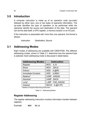
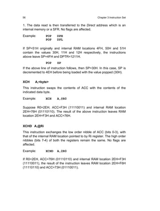
![Chapter 3 Instruction Set 49
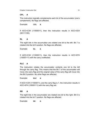
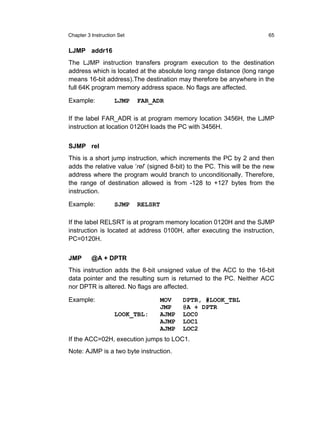
This instruction clears bits 6, 2 and 1 of output Port 1.
Mnemonic Description
ANL A, Rn A = A & [Rn]
ANL A, direct A = A & [direct memory]
ANL A,@Ri A = A & [memory pointed to by Ri]
ANL A,#data A= A & immediate data
ANL direct,A [direct] = [direct] & A
ANL direct,#data [direct] = [direct] & immediate data
ORL A, Rn A = A OR [Rn]
ORL A, direct A = A OR [direct]
ORL A,@Ri A = A OR [@RI]
ORL A,#data A = A OR immediate data
ORL direct,A [direct] = [direct] OR A
ORL direct,#data [direct] = [direct] OR immediate data
XRL A, Rn A = A XOR [Rn]
XRL A, direct A = A XOR [direct memory]
XRL A,@Ri A = A XOR [@Ri]
XRL A,#data A = A XOR immediate data
XRL direct,A [direct] = [direct] XOR A
XRL direct,#data [direct] = [direct] XOR immediate data
CLR A Clear A
CPL A Complement A
RL A Rotate A left
RLC A Rotate A left (through C)
RR A Rotate A right
RRC A Rotate A right (through C)
SWAP A Swap nibbles
Table 3.3 List of Logical Instructions](https://image.slidesharecdn.com/14157565-embedded-programming-101014045310-phpapp01/85/14157565-embedded-programming-62-320.jpg)
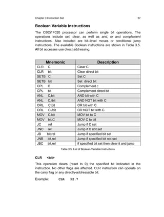
![Chapter 3 Instruction Set 53
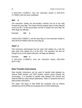
Mnemonic Description
MOV @Ri, direct [@Ri] = [direct]
MOV @Ri, #data [@Ri] = immediate data
MOV DPTR, #data 16 [DPTR] = immediate data
MOVC A,@A+DPTR A = Code byte from [@A+DPTR]
MOVC A,@A+PC A = Code byte from [@A+PC]
MOVX A,@Ri A = Data byte from external ram [@Ri]
MOVX A,@DPTR A = Data byte from external ram [@DPTR]
MOVX @Ri, A External[@Ri] = A
MOVX @DPTR,A External[@DPTR] = A
PUSH direct Push into stack
POP direct Pop from stack
XCH A,Rn A = [Rn], [Rn] = A
XCH A, direct A = [direct], [direct] = A
XCH A, @Ri A = [@Rn], [@Rn] = A
XCHD A,@Ri Exchange low order digits
Table 3.4 List of Data Transfer Instructions
MOV <dest-byte>,<source-byte>
This instruction moves the source byte into the destination location. The
source byte is not affected, neither are any other registers or flags.
Example: MOV R1,#60 ;R1=60H
MOV A,@R1 ;A=[60H]
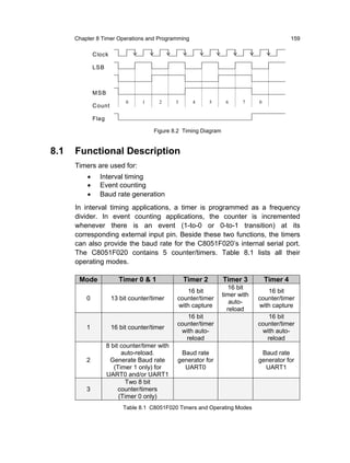
MOV R2,#61 ;R2=61H
ADD A,@R2 ;A=A+[61H]
MOV R7,A ;R7=A
If internal RAM locations 60H=10H, and 61H=20H, then after the
operations of the above instructions R7=A=30H. The data contents of
memory locations 60H and 61H remain intact.
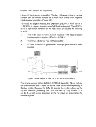
MOV DPTR, #data 16
This instruction loads the data pointer with the 16-bit constant and no
flags are affected.](https://image.slidesharecdn.com/14157565-embedded-programming-101014045310-phpapp01/85/14157565-embedded-programming-66-320.jpg)
![Chapter 3 Instruction Set 67
Example: CJNE R3,#50H,NEQU
… … ;R3 = 50H
NEQU: JC LOC1 ;If R3 < 50H
… … ;R7 > 50H
LOC1: … … ;R3 < 50H
DJNZ <byte>,<rel-addr>
This instruction is ”decrement jump not zero”. It decrements the contents
of the destination location and if the resulting value is not 0, branches to
the address indicated by the source operand. An original value of 00H
underflows to FFH. No flags are affected.
Example: DJNZ 20H,LOC1
DJNZ 30H,LOC2
DJNZ 40H,LOC3
If internal RAM locations 20H, 30H and 40H contain the values 01H, 5FH
and 16H respectively, the above instruction sequence will cause a jump
to the instruction at LOC2, with the values 00H, 5EH, and 15H in the 3
RAM locations. Note, the first instruction will not branch to LOC1
because the [20H] = 00H, hence the program continues to the second
instruction. Only after the execution of the second instruction (where the
location [30H] = 5FH), then the branching takes place.
NOP
This is the no operation instruction. The instruction takes one machine
cycle operation time. Hence it is useful to time the ON/OFF bit of an
output port.
Example: CLR P1.2
NOP
NOP
NOP
NOP
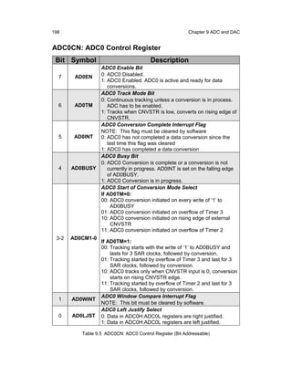
SETB P1.2](https://image.slidesharecdn.com/14157565-embedded-programming-101014045310-phpapp01/85/14157565-embedded-programming-80-320.jpg)

![76 Chapter 4 ASM Directives
DB (Define Byte)
The DB directive initializes code memory with a byte value. The directive
has the following format:
label: DB expression, expression…
Note:
label is the starting address where the byte values are stored
expression is the byte value, it can be a character string, a symbol,
or an 8-bit constant
Example:
CSEG AT 200H
MSG: DB ‘ Please enter your password’, 0
ARRAY: DB 10H, 20H,30H,40H,50H
The above string of characters will be stored as ASCII bytes starting from
location 200H, which means location [200H]=50H, [201H]=6CH and so
on.
Notice that the DB directive is declared in a code segment. If it is defined
in a different segment, the assembler will generate an error.
DW (Define Word)
The DW directive initializes the code memory with a double byte or a 16-
bit word. The DW directive has the following format:
label: DW expression ,expression…](https://image.slidesharecdn.com/14157565-embedded-programming-101014045310-phpapp01/85/14157565-embedded-programming-89-320.jpg)
![Chapter 4 ASM Directives 81
4.6 Tutorial Questions
1. Give an example of the following:
(a) Absolute Segment directive
(b) Memory Initialization directive
(c) Relocatable Segment directive
2. Correct the error in the following instructions:]
(a) DSEG AT 0300H
VAL: DB 1
(b) PAR : EQU 200
3. Write a short program in a relocatable segment to do the following
task:
Add the values from register R0 and R3 of Bank 2 and output the
sum to Port3
4. If there is a need for keyboard interfacing upon execution of the
program, what sort of directives would be most suitable to be
declared in the program in order to perform the above task?
5. Name the type of memory where the following assembler
directives can be defined.
ORG 10H
DB 61H, 62H, 63H
DW ‘0’,’1’,’2’
6. What is the advantage of using EQU directive in an assembly
language program?](https://image.slidesharecdn.com/14157565-embedded-programming-101014045310-phpapp01/85/14157565-embedded-programming-94-320.jpg)

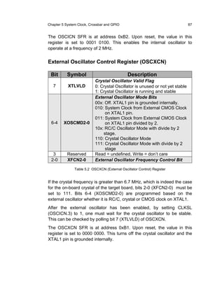
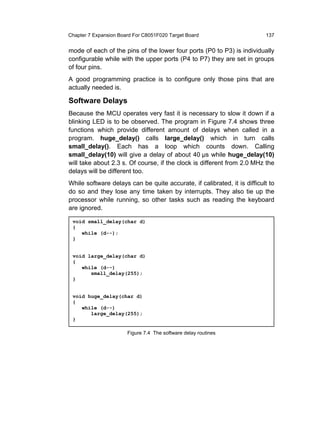
![90 Chapter 5 System Clock, Crossbar and GPIO
Example:
CLR EA ;disable all interrupts
MOV WDTCN, #0DEH ;disable WDT
MOV WDTCN, #0ADH ;disable WDT
SETB EA ;enable interrupts
Setting WDT Interval
Bits 2-0 of WDTCN control the watchdog timeout interval. The interval is
given by the following equation:
43+WDTCN [2-0] x Tsysclk
Tsysclk is the system clock period. For a 2 MHz system clock, the interval
range that can be programmed is 0.032 ms to 524 ms. When the
Watchdog Timeout Interval Bits are written to the WDTCN register, the
WDTCN.7 bit must be held at logic 0. The programmed interval may be
read back by reading the WDTCN register. After a reset, WDTCN[2-0]
reads 111b.
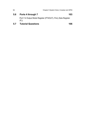
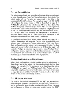
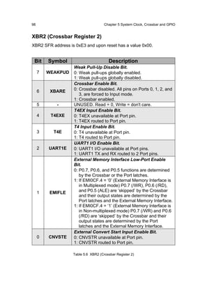
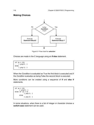
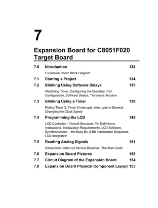
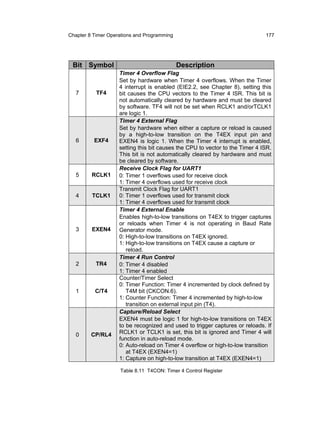
5.3 Digital Crossbar
The C8051F020 has a rich set of digital resources like UARTs, System
Management Bus (SMBus),Timer control inputs and interrupts. However,
these peripherals do not have dedicated pins through which they may be
accessed. Instead they are available through the four lower I/O ports
(P0, P1, P2 and P3). Each of the pins on P0, P1, P2 and P3 can be
defined as a General Purpose Input/Output (GPIO) pin or can be
controlled by a digital peripheral. Thus the lower ports have dual
functionalities. Based on the application, a system designer would have
to decide what capabilities are required and then allocate the necessary
digital functions to the port pins. This flexibility makes the MCU very
versatile. The resource allocation is controlled by programming the
Priority Crossbar Decoder, simply called the “Crossbar”. The port pins
are allocated and assigned to the digital peripherals using a priority
order. Figure 5.2 is the functional block diagram showing the priority
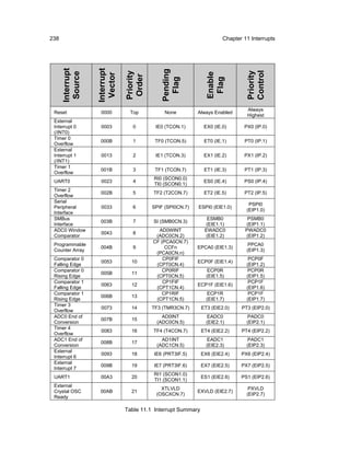
decoder, lower ports and the digital resources that may be controlled.](https://image.slidesharecdn.com/14157565-embedded-programming-101014045310-phpapp01/85/14157565-embedded-programming-103-320.jpg)
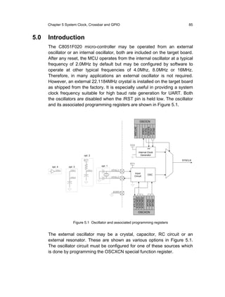
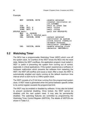
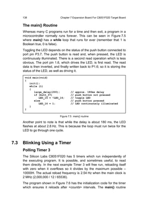
![92 Chapter 5 System Clock, Crossbar and GPIO
assigned together. Each combination of enabled peripherals results in a
unique device pin-out.
P0 P1 P2 P3
Crossbar Register Bits
Pin I/O 0 1 2 3 4 5 6 7 0 1 2 3 4 5 6 7 0 1 2 3 4 5 6 7 0 1 2 3 4 5 6 7
Tx0 ●
UART0EN: XBR0.2
Rx0 ●
SCK ● ●
MISO ● ●
SPI0EN: XBR0.1
MOSI ● ●
NSS ● ●
SDA ● ● ● ●
SMB0EN: XBR0.0
SCL ● ● ● ●
TX1 ● ● ● ● ●
UART1EN: XBR2.2
RX1 ● ● ● ● ● ●
CEX0 ● ● ● ● ● ● ●
CEX1 ● ● ● ● ● ● ● ●
CEX2 ● ● ● ● ● ● ● ● PCA0ME: XBR0.[5:3]
CEX3 ● ● ● ● ● ● ● ● ●
CEX4 ● ● ● ● ● ● ● ● ●
ECI ● ● ● ● ● ● ● ● ● ● ● ● ● ● ● ● ECI0E: XBR0.6
CP0 ● ● ● ● ● ● ● ● ● ● ● ● ● ● ● ● ● CP0E: XBR0.7
CP1 ● ● ● ● ● ● ● ● ● ● ● ● ● ● ● ● ● ● CP1E: XBR1.0
T0 ● ● ● ● ● ● ● ● ● ● ● ● ● ● ● ● ● ● ● T0E: XBR1.1
/INT0 ● ● ● ● ● ● ● ● ● ● ● ● ● ● ● ● ● ● ● ● INT0E: XBR1.2
T1 ● ● ● ● ● ● ● ● ● ● ● ● ● ● ● ● ● ● ● ● ● T1E: XBR1.3
/INT1 ● ● ● ● ● ● ● ● ● ● ● ● ● ● ● ● ● ● ● ● ● ● INT1E: XBR1.4
T2 ● ● ● ● ● ● ● ● ● ● ● ● ● ● ● ● ● ● ● ● ● ● ● T2E: XBR1.5
T2EX ● ● ● ● ● ● ● ● ● ● ● ● ● ● ● ● ● ● ● ● ● ● ● ● T2EXE: XBR1.6
T4 ● ● ● ● ● ● ● ● ● ● ● ● ● ● ● ● ● ● ● ● ● ● ● ● ● T4E: XBR2.3
T4EX ● ● ● ● ● ● ● ● ● ● ● ● ● ● ● ● ● ● ● ● ● ● ● ● ● ● T4EXE: XBR2.4
/SYSCLK ● ● ● ● ● ● ● ● ● ● ● ● ● ● ● ● ● ● ● ● ● ● ● ● ● ● ● SYSCKE: XBR1.7
CNVSTR ● ● ● ● ● ● ● ● ● ● ● ● ● ● ● ● ● ● ● ● ● ● ● ● ● ● ● ● CNVSTE: XBR2.0
AIN1.2/A10
AIN1.3/A11
AIN1.4/A12
AIN1.5/A13
AIN1.6/A14
AIN1.7/A15
AIN1.0/A8
AIN1.1/A9
A10m/A2
A11m/A3
A12m/A4
A13m/A5
A14m/A6
A15m/A7
A8m/A0
A9m/A1
AD0/D0
AD1/D1
AD2/D2
AD3/D3
AD4/D4
AD5/D5
AD6/D6
AD7/D7
/WR
ALE
/RD
AIN1 Inputs / Muxed Addr H / Muxed Data /
Mon-Muxed Addr H Non-Muxed Addr L Non-Muxed Data
Figure 5.3 Digital Crossbar Priority Decode Table
The output states of port pins that are allocated by the crossbar are
controlled by the digital peripheral that is mapped to those pins and
hence Writes to the Port Data registers (or associated Port bits) will have
no effect on the states of the pins. The Port pins on Port 0 to 3 that are
not allocated by the Crossbar may be accessed as General-Purpose I/O
pins by reading and writing the associated Port Data registers.](https://image.slidesharecdn.com/14157565-embedded-programming-101014045310-phpapp01/85/14157565-embedded-programming-105-320.jpg)
![Chapter 5 System Clock, Crossbar and GPIO 99
P0 (Port0 Data Register)
P0 SFR address is 0x80 and upon reset has a value 0xFF.
Bit Symbol Description
Port0 Output Latch Bits.
(Write - Output appears on I/O pins per XBR0,
XBR1, XBR2, and XBR3 Registers)
0: Logic Low Output.
7-0 P0.[7:0] 1: Logic High Output (open if corresponding
P0MDOUT.n bit = 0).
(Read - Regardless of XBR0, XBR1, XBR2, and
XBR3 Register settings).
0: P0.n pin is logic low.
1: P0.n pin is logic high.
Table 5.7 P0 (Port0 Data Register)
P0MDOUT (Port0 Output Mode Register)
P0MDOUT SFR address is 0xA4 and upon reset has a value 0x00.
Bit Symbol Description
Port0 Output Mode Bits.
0: Port Pin output mode is configured as
7-0 P0MDOUT.[7:0] Open-Drain.
1: Port Pin output mode is configured as
Push-Pull.
Table 5.8 P0MDOUT (Port0 Output Mode Register)](https://image.slidesharecdn.com/14157565-embedded-programming-101014045310-phpapp01/85/14157565-embedded-programming-112-320.jpg)
![100 Chapter 5 System Clock, Crossbar and GPIO
P1 (Port1 Data Register)
P1 SFR address is 0x90 and upon reset has a value 0xFF.
Bit Symbol Description
Port1 Output Latch Bits.
(Write - Output appears on I/O pins per XBR0, XBR1,
XBR2, and XBR3 Registers)
0: Logic Low Output.
7-0 P1.[7:0] 1: Logic High Output (open if corresponding
P1MDOUT.n bit = 0).
(Read - Regardless of XBR0, XBR1, XBR2, and XBR3
Register settings).
0: P1.n pin is logic low.
1: P1.n pin is logic high.
Table 5.9 P1 (Port1 Data Register)
P1MDOUT (Port1 Output Mode Register)
P1MDOUT SFR address is 0xA5 and upon reset has a value 0x00.
Bit Symbol Description
Port1 Output Mode Bits.
0: Port Pin output mode is configured as
7-0 P1MDOUT.[7:0] Open-Drain.
1: Port Pin output mode is configured as
Push-Pull.
Table 5.10 P1MDOUT (Port1 Output Mode Register)
P1MDIN (Port1 Input Mode Register)
P1MDIN SFR address is 0xBD and upon reset has a value 0xFF.
Bit Symbol Description
Port 1 Input Mode Bits.
0: Port Pin is configured in Analog Input
mode. The digital input path is disabled (a
read from the Port bit will always return ‘0’).
7-0 P1MDIN.[7:0] The weak pull-up on the pin is disabled.
1: Port Pin is configured in Digital Input mode.
A read from the Port bit will return the logic
level at the Pin. The state of the weak pull-up is
determined by the WEAKPUD bit
Table 5.11 P1MDIN (Port1 Input Mode Register)](https://image.slidesharecdn.com/14157565-embedded-programming-101014045310-phpapp01/85/14157565-embedded-programming-113-320.jpg)
![Chapter 5 System Clock, Crossbar and GPIO 101
P2 (Port2 Data Register)
P2 SFR address is 0xA0 and upon reset has a value 0xFF.
Bit Symbol Description
Port2 Output Latch Bits.
(Write - Output appears on I/O pins per XBR0,
XBR1, XBR2, and XBR3 Registers)
0: Logic Low Output.
7-0 P0.[7:0] 1: Logic High Output (open if corresponding
P2MDOUT.n bit = 0).
(Read - Regardless of XBR0, XBR1, XBR2, and
XBR3 Register settings).
0: P2.n pin is logic low.
1: P2.n pin is logic high.
Table 5.12 P2 (Port2 Data Register)
P2MDOUT (Port2 Output Mode Register)
P2MDOUT SFR address is 0xA6 and upon reset has a value 0x00.
Bit Symbol Description
Port2 Output Mode Bits.
0: Port Pin output mode is configured as
7-0 P2MDOUT.[7:0] Open-Drain.
1: Port Pin output mode is configured as
Push-Pull.
Table 5.13 P2MDOUT (Port2 Output Mode Register)](https://image.slidesharecdn.com/14157565-embedded-programming-101014045310-phpapp01/85/14157565-embedded-programming-114-320.jpg)
![102 Chapter 5 System Clock, Crossbar and GPIO
P3 (Port3 Data Register)
P3 SFR address is 0xB0 and upon reset has a value 0xFF.
Bit Symbol Description
Port3 Output Latch Bits.
(Write - Output appears on I/O pins per XBR0,
XBR1, XBR2, and XBR3 Registers)
0: Logic Low Output.
7-0 P3.[7:0] 1: Logic High Output (open if corresponding
P3MDOUT.n bit = 0).
(Read - Regardless of XBR0, XBR1, XBR2, and
XBR3 Register settings).
0: P3.n pin is logic low.
1: P3.n pin is logic high.
Table 5.14 P3 (Port3 Data Register)
P3MDOUT (Port3 Output Mode Register)
P3MDOUT SFR address is 0xA7 and upon reset has a value 0x00.
Bit Symbol Description
Port3 Output Mode Bits.
0: Port Pin output mode is configured as
7-0 P3MDOUT.[7:0] Open-Drain.
1: Port Pin output mode is configured as
Push-Pull.
Table 5.15 P3MDOUT (Port3 Output Mode Register)](https://image.slidesharecdn.com/14157565-embedded-programming-101014045310-phpapp01/85/14157565-embedded-programming-115-320.jpg)
![104 Chapter 5 System Clock, Crossbar and GPIO
The SFRs associated with Ports 7 to 4 are P74OUT and the individual
Port Data registers, P4, P5, P6 and P7. These SFRs are described next.
P74OUT (Ports 7-4 Output Mode Register)
P74OUT SFR address is 0xB5 and upon reset has a value 0x00.
Bit Symbol Description
Port7 Output Mode High Nibble Bit.
7 P7H 0: P7.[7:4] configured as Open-Drain.
1: P7.[7:4] configured as Push-Pull.
Port7 Output Mode Low Nibble Bit.
6 P7L 0: P7.[3:0] configured as Open-Drain.
1: P7.[3:0] configured as Push-Pull.
Port6 Output Mode High Nibble Bit.
5 P6H 0: P6.[7:4] configured as Open-Drain.
1: P6.[7:4] configured as Push-Pull.
Port6 Output Mode Low Nibble Bit.
4 P6L 0: P6.[3:0] configured as Open-Drain.
1: P6.[3:0] configured as Push-Pull.
Port5 Output Mode High Nibble Bit.
3 P5H 0: P5.[7:4] configured as Open-Drain.
1: P5.[7:4] configured as Push-Pull.
Port5 Output Mode Low Nibble Bit.
2 P5L 0: P5.[3:0] configured as Open-Drain.
1: P5.[3:0] configured as Push-Pull.
Port4 Output Mode High Nibble Bit.
1 P4H 0: P4.[7:4] configured as Open-Drain.
1: P4.[7:4] configured as Push-Pull.
Port4 Output Mode Low Nibble Bit.
0 P4L 0: P4.[3:0] configured as Open-Drain.
1: P4.[3:0] configured as Push-Pull.
Table 5.17 P74OUT (Port 7-4 Output Mode Register)](https://image.slidesharecdn.com/14157565-embedded-programming-101014045310-phpapp01/85/14157565-embedded-programming-117-320.jpg)
![Chapter 5 System Clock, Crossbar and GPIO 105
Px (Ports x Data Register)
x is 4 to 7. P4, P5, P6 and P7 SFR addresses are 0x84, 0x85, 0x86 and
0x96 respectively and upon reset have a value 0xFF.
Bit Symbol Description
Portx Output Latch Bits.
Write - Output appears on I/O pins.
0: Logic Low Output.
7-0 Px.[7:0] 1: Logic High Output (Open-Drain if corresponding
P74OUT bit = 0).
Read - Returns states of I/O pins.
0: Px.n pin is logic low.
1: Px.n pin is logic high.
Table 5.18 Px (Port x Data Register)](https://image.slidesharecdn.com/14157565-embedded-programming-101014045310-phpapp01/85/14157565-embedded-programming-118-320.jpg)
![106 Chapter 5 System Clock, Crossbar and GPIO
5.7 Tutorial Questions
1. Four toggle switches (SW3, SW2, SW1 and SW0) are connected
to Port 2 [7:4]. Four LEDs (LED3, LED2, LED1, and LED0) are
connected to Port 3 [3:0]. Write the code to initialize the ports
accordingly. The output port pins for LED must be in push-pull
mode. Disable global weak pull-ups. If only a part of the port is
used, make sure that the configuration and mode of the unused
pins are not disturbed.
2. When a toggle switch is ON, it presents a logic 0 at the Port 2
input. A LED turns ON when a logic 1 is set at the Port 3 output
pin. If a switch (SW3 .. SW0) is ON, the corresponding LED
(LED3 .. LED0) should be turned ON; OFF otherwise. Write the
code to read the status of the switches and turn ON/OFF the
respective LEDs.
3. What are the various external oscillator circuits that may be
connected to the C8051F020 micro-controller and how do these
affect the programming bits in the OSCXCN register?
4. Write a function to initialize the clock to use the internal oscillator
at 8 MHz. The function prototype is -
void Init_Int_Osc(void);
The missing clock detector has to be disabled.
5. The C8051F020 micro-controller is to be connected to receive
commands from a peripheral device using UART1 serial
communication in Mode 1 at 9600 baud rate. Timer 4 is used to
generate the baud rate. System Clock used is 22.1184 MHz
external crystal oscillator.
(a) Write a function to configure and enable the crossbar and
Port 0 for UART1 communication. Transmit pin is to be set in
push-pull mode. The function prototype is -
void Init_Port(void);
(You can assume that UART0 is unused)](https://image.slidesharecdn.com/14157565-embedded-programming-101014045310-phpapp01/85/14157565-embedded-programming-119-320.jpg)


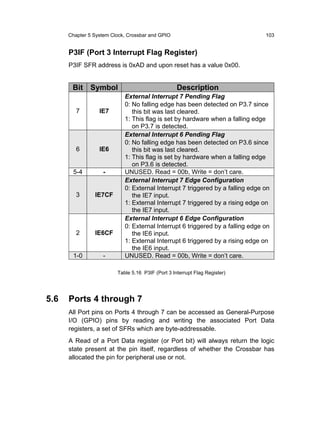
![136 Chapter 7 Expansion Board For C8051F020 Target Board
function disable the WDT, which avoids the overhead of regularly
resetting it.
void init(void)
{
WDTCN = 0xDE; // Watchdog Timer Ctrl Register
WDTCN = 0xAD; // Disable watch dog timer
//---- Configure the XBRn Registers
XBR0 = 0x00; //
XBR1 = 0x00; // Enable the crossbar,
XBR2 = 0x40; // weak pullups enabled
//---- Port configuration (1 = Push Pull Output)
P0MDOUT = 0x00; // Output configuration for P0
P1MDOUT = 0x40; // Output configuration for P1,
// LED_16 is push pull
P2MDOUT = 0x00; // Output configuration for P2
P3MDOUT = 0x00; // Output configuration for P3
P74OUT = 0x48; // Output configuration for P4-7
// (P7[0..3] push pull)
P5 |= 0x0F; //- P5[3:0] Open Drain used as input
P4 = 0xFF; //- P4 Open Drain used as input
}
Figure 7.3 Initializing Internal Registers
To disable the WDT, two writes are needed to the watch dog timer
control register (WDTCN). These must occur within 4 clock cycles of
each other so interrupts should not be enabled at the time.
Configuring the Crossbar
The crossbar is controlled by three registers - XBR0, XBR1 and XBR2. It
is rather complex to setup the crossbar and a good approach is to use
the Silicon Labs’ Configuration Utility software to select the mapping you
require. In this example the only bit which needs to be set is in XBR2
called XBARE – Cross Bar Enable. If the crossbar is not enabled, all the
port pins remain as inputs only so an LED cannot be driven.
Port Configuration
With the crossbar enabled, the port pins will pull high via the internal
resistors, allowing the pin to source a few µA, when a logic 1 is written to
the pin. Internal transistors will pull the pin low in response to a logic 0
allowing it to sink up to 50 mA. The LED on P1.6 and the four LEDs on
the expansion board must be driven high to illuminate and so the port
pins that drive them need to be configured in push-pull output mode.
They can then easily source the required 10 mA for the LED. The output](https://image.slidesharecdn.com/14157565-embedded-programming-101014045310-phpapp01/85/14157565-embedded-programming-149-320.jpg)
![144 Chapter 7 Expansion Board For C8051F020 Target Board
resistors. With an 8051F020 this is done by NOT using push-pull outputs
on the LCD data port, globally enabling weak pull-ups, and writing FFH
to the data port before attempting to read it.
Many microcontrollers are able to drive their pins much faster than the
HD44780 is able to read them. For example, the C8051F020 can toggle
a pin in 90 ns when running off its 22 MHz crystal while the HD44780
has minimum pulse requirements of almost 1us. Some sort of delay must
be built into your program to ensure your commands reach the LCD.
Pin Full
Signal Function
Number Name
VSS 1 Ground 0V common connection
Supply
VDD 2 +5V supply
Voltage
When varied between 0 and VSS
VO 3 Contrast
changes the optimum viewing angle.
↑ (low to high transaction) The LCD
controller reads the state of RS
and RW
Note: to write from the LCD (e.g. the
E 6 Enable
busy bit – see later) E should
remain high.
↓ (high to low transaction) The LCD
controller reads the data bus
Register 0: Instruction Register
RS 4 Select 1: Data Register
Read or 0: Write to LCD
RW 5 Write 1: Read from LCD
8-bit Data To convey instructions or data to the
D[0..7] 7 - 14 Bus LCD controller
15,16 No Connection
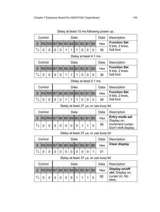
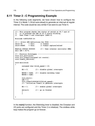
Figure 7.12 LCD Module Pin Definitions
Instructions
Instructions are used for configuring the LCD controller, to pass it data
which will be displayed, and to read status information back from it.
Figure 7.13 shows the instructions in numerical order.](https://image.slidesharecdn.com/14157565-embedded-programming-101014045310-phpapp01/85/14157565-embedded-programming-157-320.jpg)
![Chapter 7 Expansion Board For C8051F020 Target Board 145
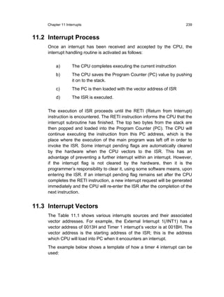
Control Data Bits
Exec
R R Time
Instruction E 7 6 5 4 3 2 1 0 Description
S W
(µs)
Clears entire display. Sets DDRAM
Clear Display ↑↓ 0 0 0 0 0 0 0 0 0 1 1520
address counter to zero.
Sets DDRAM address counter to
Return Home ↑↓ 0 0 0 0 0 0 0 0 1 - zero and returns display to original 1520
position if shifted.
Sets how curser and display will
Entry Mode move when data is written.
↑↓ 0 0 0 0 0 0 0 1 I/D S 37
SET I/D=1: Increment, ID=0: Decrement
S=1: shift display
Controls visibility of display, curser
Display On/Off and blinking feature.
↑↓ 0 0 0 0 0 0 1 D C B 37
Control D=1: display on, C=1: curser on,
B=1: curser character blinks
Moves curser or shifts display.
Cursor or S/C=1, display shift, S/C=0, curser
↑↓ 0 0 0 0 0 S/C R/L - - 37
Display Shift move
R/L=1, right shift, R/L=0, left shift
Interface data length (DL=1:8
bits, DL=0: 4 bits)
Number of display lines (N=1:2lines,
Function Set ↑↓ 0 0 0 0 1 DL N F - - 37
N=0,1:line)
Character Font (F=1:5x10 dots,
F=0,5x8 dots)
Character Generator RAM address.
Set CGRAM
↑↓ 0 0 0 1 b[5..0] Address CGRAM data is sent and received 37
Address
following this command
Display Data RAM address. DDRAM
Set DDRAM
↑↓ 0 0 1 b[6..0] Address data is sent and received following 37
Address
this command
BF=1 indicates internal operation
Read Busy still being performed. Also returns
Flag & ↑1 0 1 BF Address Counter address counter contents (CG or DD 37
Address RAM, depending on what was last
accessed)
Write to
↑↓ 1 0 b[7..0] write data Writes data to CG or DD RAM 37
RAM
Read from
↑↓ 1 1 b[7..0] read data Reads data from CG or DD RAM 37
RAM
Figure 7.13 Hitachi HD44780 Instruction Set
Instructions are conveyed to the LCD controller by setting RS and RW as
listed and setting E high then low. The data is clocked into the controller
on the falling edge (↓).
Initialization Requirements
When the power is first applied to a HD44780 based module it will self
initialize provided the power supply rises at the correct rate. Interestingly
the default wakeup state has the display off! With a normal power supply,](https://image.slidesharecdn.com/14157565-embedded-programming-101014045310-phpapp01/85/14157565-embedded-programming-158-320.jpg)

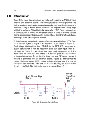
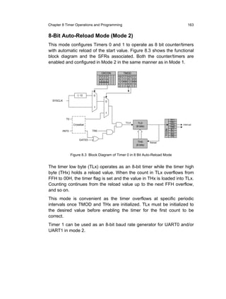
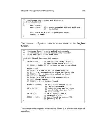
![Chapter 8 Timer Operations and Programming 169
In Baud Rate Generator mode, the Timer z time base is the system clock
divided by two. When selected as the UARTx baud clock source, Timer z
defines the UARTx baud rate as follows:
SYSCLK
BaudRate =
(65536 − [ RCAPzH , RCAPzL ]) × 32
If a different time base is required, setting the C/Tz bit to 1 will allow the
time base to be derived from the external input pin Tz. In this case, the
baud rate for the UART is calculated as:
FCLK
BaudRate =
(65536 − [ RCAPzH , RCAPzL ]) × 16
where FCLK is the frequency of the signal (TCLK) supplied to Timer z and
[RCAPzH, RCAPzL] is the 16 bit value held in the capture registers.
Figure 8.9 Block Diagram of Timer 4 in Baud Rate Generation Mode (Mode 2)](https://image.slidesharecdn.com/14157565-embedded-programming-101014045310-phpapp01/85/14157565-embedded-programming-182-320.jpg)

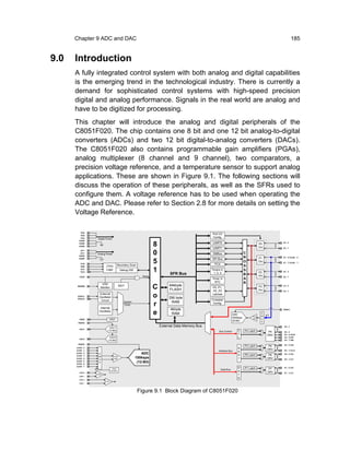
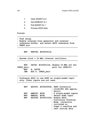
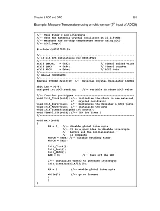
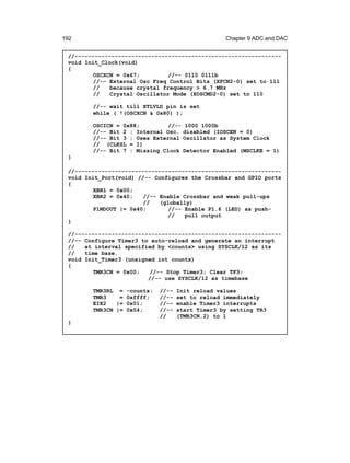
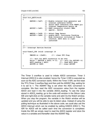
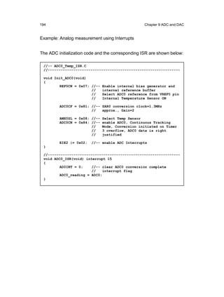
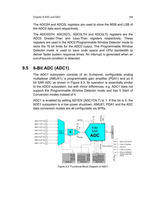
![Chapter 9 ADC and DAC 187
programmed for gains of 0.5, 1, 2, 4, 8 or 16. The gain defaults to 1 on
reset.
Starting ADC0 Conversions
Conversions can be started in four different ways, depending on the
AD0CM1 and AD0CM0 bits in ADC0CN (Table 9.5). These are:
1) Software command (Writing 1 to AD0BUSY)
2) Overflow of Timer 2
3) Overflow of Timer 3
4) External signal input (rising edge of CNVSTR).
The AD0BUSY bit remains set to 1 during conversion and restored to 0
when the conversion is complete. The falling edge of AD0BUSY triggers
an interrupt (when enabled) and sets the AD0INT interrupt flag.
Converted data is stored in the ADC0H and ADC0L registers and can be
either left or right justified in the register pair depending on the
programmed state of the AD0LJST (ADC0CN.0) bit.
ADC0H[3:0]:ADC0L[7:0], if AD0LJST = 0
(ADC0H[7:4] will be the sign-extension of ADC0H.3 for a differential
reading, otherwise = 0000b).
ADC0H[7:0]:ADC0L[7:4], if AD0LJST = 1
(ADC0L[3:0] = 0000b).
Example:
If the ADC0 output data word = FFFH (111111111111b) & AD0LJST = 0:
ADC0H:ADC0L = 0FFFH (0000111111111111)
If AD0LJST = 1:
ADC0H:ADC0L = FFF0H (1111111111110000b)](https://image.slidesharecdn.com/14157565-embedded-programming-101014045310-phpapp01/85/14157565-embedded-programming-200-320.jpg)
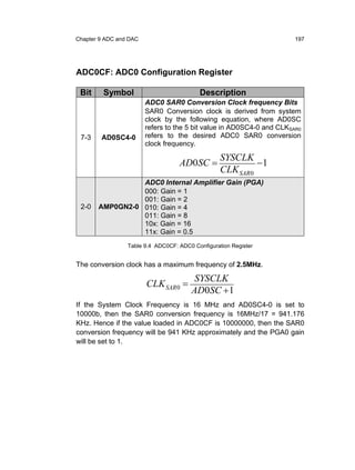
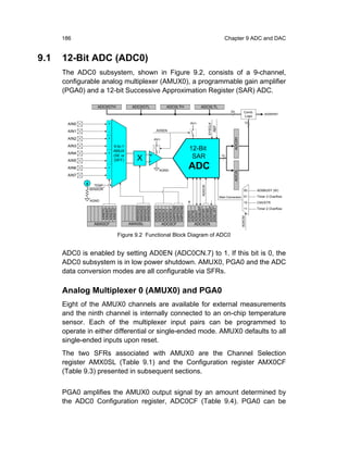
![210 Chapter 9 ADC and DAC
Output Scaling
The format of the 12 bit data word in the DACxH and DACxL registers
can be configured by setting the appropriate DACxDF bits
(DACxCN.[2:0]). The five data word orientations are shown in Figure 9.5.
DACxDF2-0 = 000:
DACxH DACxL
MSB LSB
001:
DACxH DACxL
MSB LSB
010:
DACxH DACxL
MSB LSB
011:
DACxH DACxL
MSB LSB
1xx:
DACxH DACxL
MSB LSB
Figure 9.5 DAC Data Format
9.10 Programming the DACs
DACx can be programmed through the following sequence:
1) Configure the voltage reference (REF0CN).
2) Load the data word registers with the desired 12 bit digital value
(DACxH and DACxL).
3) Set the appropriate output scheduling mode and data word
format, and turn on DACx (DACxCN.7).
4) Set up and run the appropriate timers if applicable.](https://image.slidesharecdn.com/14157565-embedded-programming-101014045310-phpapp01/85/14157565-embedded-programming-223-320.jpg)
![212 Chapter 9 ADC and DAC
9.11 DAC0 SFRs
DAC0CN: DAC0 Control Register
Bit Symbol Description
DAC0 Enable Bit
0: DAC0 disabled. DAC0 is in low power
7 DAC0EN shutdown mode and the output pin is in a high
impedance state.
1: DAC0 enabled. DAC0 is operational and the
output pin is active.
6-5 - UNUSED. Read=00, Write=don’t care
DAC0 Mode Bits
00: DAC output updates occur on write to
DAC0H.
01: DAC output updates occur on Timer 3
4-3 DAC0MD1-0 overflow.
10: DAC output updates occur on Timer 4
overflow.
11: DAC output updates occur on Timer 2
overflow.
DAC0 Data Format Bits. See Figure 9.5
000: The most significant 4 bits of the DAC0
Data Word are in DAC0H[3:0], while the
least significant 8 bits are in DAC0L[7:0].
001: The most significant 5 bits of the DAC0
Data Word are in DAC0H[4:0], while the
least significant 7 bits are in DAC0L[7:1].
2-0 DAC0DF2-0 010: The most significant 6 bits of the DAC0
Data Word are in DAC0H[5:0], while the
least significant 6 bits are in DAC0L[7:2].
011: The most significant 7 bits of the DAC0
Data Word are in DAC0H[6:0], while the
least significant 5 bits are in DAC0L[7:3].
1xx: The most significant 8 bits of the DAC0 Data
Word are in DAC0H[7:0], while the least
significant 4 bits are in DAC0L[7:4].
Table 9.9 DAC0CN: DAC0 Control Register
DAC0H and DAC0L are used to store the most significant and least
significant DAC0 data word respectively.](https://image.slidesharecdn.com/14157565-embedded-programming-101014045310-phpapp01/85/14157565-embedded-programming-225-320.jpg)
![Chapter 9 ADC and DAC 213
9.12 DAC1 SFRs
DAC1CN: DAC1 Control Register
Bit Symbol Description
DAC1 Enable Bit
0: DAC1 disabled. DAC1 is in low power
7 DAC1EN shutdown mode and the output pin is in a high
impedance state.
1: DAC1 enabled. DAC1 is operational and the
output pin is active.
6-5 - UNUSED. Read=00, Write=don’t care
DAC1 Mode Bits
00: DAC output updates occur on write to DAC1H.
01: DAC output updates occur on Timer 3
4-3 DAC1MD1-0 overflow.
10: DAC output updates occur on Timer 4
overflow.
11: DAC output updates occur on Timer 2
overflow.
DAC1 Data Format Bits. See Figure 9.5
000: The most significant 4 bits of the DAC1 Data
Word are in DAC1H[3:0], while the least
significant 8 bits are in DAC1L[7:0].
001: The most significant 5 bits of the DAC1 Data
Word are in DAC1H[4:0], while the least
significant 7 bits are in DAC1L[7:1].
2-0 DAC1DF2-0 010: The most significant 6 bits of the DAC1 Data
Word are in DAC1H[5:0], while the least
significant 6 bits are in DAC1L[7:2].
011: The most significant 7 bits of the DAC1 Data
Word are in DAC1H[6:0], while the least
significant 5 bits are in DAC1L[7:3].
1xx: The most significant 8 bits of the DAC1 Data
Word are in DAC1H[7:0], while the least
significant 4 bits are in DAC1L[7:4].
Table 9.10 DAC1CN: DAC1 Control Register
DAC1H and DAC1L are used to store the most significant and least
significant DAC1 data word respectively.](https://image.slidesharecdn.com/14157565-embedded-programming-101014045310-phpapp01/85/14157565-embedded-programming-226-320.jpg)

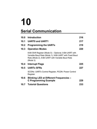
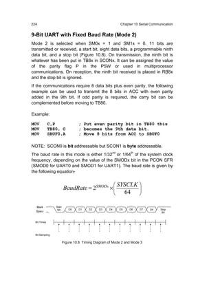
![222 Chapter 10 Serial Communication
A possible application of this mode is to expand the output capability of
the chip. A serial-to-parallel shift register IC can be connected to the TXx
and RXx pins to provide an extra 8 output lines as shown in Figure 10.5.
Additional shift registers may be cascaded to the first for further
expansion.
In Mode 0, an external pull-up is typically required because RXx is forced
to open-drain.
8-Bit UART with Variable Baud Rate (Mode 1)
Mode 1 is selected when SM0x = 0 and SM1x = 1. It provides standard
asynchronous, full duplex serial communication. 10 bits are transmitted
on TXx or received on RXx for each data byte. These consist of a start
bit (always 0), the eight data bits (LSB first), and a stop bit (always 1).
For a receive operation, the eight data bits are stored in SBUFx and the
stop bit goes into RB8x (SCONx.2).
The baud rate is set by the overflow rate of Timer 1, Timer 2 (UART0) or
Timer 4 (UART1), or a combination of two (T1 and T2, or T1 and T4),
one for transmit and the other for receive. The UARTs can use Timer 1
operating in 8-Bit Auto-Reload Mode, or Timers 2 or 4 operating in
Baud Rate Generator Mode to generate the baud rate. The TXx and
RXx clocks are selected separately. If TCLKx and/or RCLKx (in T2CON /
T4CON register) are set to logic 0, Timer 1 acts as the baud rate source
for the TXx and/or RXx circuits, respectively. Please refer to Chapter 8
for complete timer configuration details.
The Mode 1 baud rate equations are shown below (for the use of Timer 1
and for the use of Timer 2 or 4), where T1M is the Timer 1 Clock Select
bit (CKCON), TH1 is the 8-bit reload register for Timer 1, SMODx is the
UARTx baud rate doubler (register PCON) and [RCAPzH , RCAPzL] is
the 16-bit reload register for Timers 2 or 4. z = 2 or 4.
⎛ 2SMODx ⎞ ⎛ SYSCLK ×12(T 1M −1) ⎞
BaudRate = ⎜
⎜ 32 ⎟ ⎜ ⎟
×⎜ ⎟ for Timer 1
⎝ ⎠ ⎝ 256 − TH1 ⎟
⎠](https://image.slidesharecdn.com/14157565-embedded-programming-101014045310-phpapp01/85/14157565-embedded-programming-235-320.jpg)
![Chapter 10 Serial Communication 223
SYSCLK
BaudRate = for Timer 2 or 4
32 × (65536 − [RCAPzH , RCAPzL ])
Data transmission is initiated by writing to SBUFx. Data are shifted onto
TXx beginning with the start bit, followed by the eight data bits, then the
stop bit. The period for each bit is the reciprocal of the baud rate as
programmed in the timer. The TIx Transmit Interrupt Flag (SCONx.1) is
set at the beginning of the stop-bit time.
Data reception can begin any time after the RENx Receive Enable bit
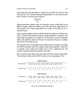
(SCONx.4) is set to 1. Reception is initiated by a 1-to-0 transition on
RXx. The incoming bit stream is sampled in the middle of each bit period
(Figure 10.7). The receiver includes “false start bit detection”, ensuring
that a start bit is valid and not triggered by noise. This works by requiring
a stop bit to be detected eight counts after the first 1-to-0 transition. If this
does not occur, it is assumed that the 1-to-0 transition was triggered by
noise and is not a valid start bit. The receiver is reset and returns to the
idle state, looking for the next 1-to-0 transition.
Mark Start
Bit D0 D1 D2 D3 D4 D5 D6 D7 Stop
Space Bit
Bit Times
Bit Sampling
Figure 10.7 Timing Diagram of Mode 1
If a valid start bit was detected, character reception continues. The start
bit is skipped, the 8 data bits are stored in SBUFx, the stop bit is stored
in RB8x and the RIx flag is set. However, these only occur if the following
conditions exist:
1. RIx = 0
2. SM2x = 0 (stop bit ignored) or SM2x = 1 and the received stop bit = 1
If these conditions are not met, SBUFx and RB8x will not be loaded and
the RIx flag will not be set. An interrupt will occur if enabled when either
TIx or RIx is set. The requirement that RIx = 0 ensures that software has
read the previous character (and cleared RIx).](https://image.slidesharecdn.com/14157565-embedded-programming-101014045310-phpapp01/85/14157565-embedded-programming-236-320.jpg)


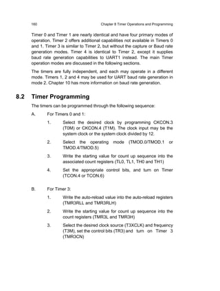
This document provides an overview of embedded programming with field-programmable mixed-signal microcontrollers. It begins with a brief introduction and then discusses embedded programming using the Silicon Labs C8051F020 microcontroller as an example platform. Key topics covered include the microcontroller's memory organization, I/O ports, analog-to-digital converters, digital-to-analog converters, and voltage reference.


![[Scholar.geology physical geography-botany] fundamentals of soil science (hen...](https://cdn.slidesharecdn.com/ss_thumbnails/scholar-geology-physicalgeography-botanyfundamentalsofsoilsciencehenryfoth-1990-8ed-380pp-ebook-121119041700-phpapp01-thumbnail.jpg?width=640&height=640&fit=bounds)