Integrator OP Amp
•
1 like•1,997 views

Integrator OP Amp, The AC or Continuous Op-amp Integrator, The AC Op-amp Integrator with DC Gain Control

Recommended
More Related Content
What's hot
What's hot (20)
Similar to Integrator OP Amp
Similar to Integrator OP Amp (20)
More from Dr.Raja R
More from Dr.Raja R (20)
Recently uploaded
Recently uploaded (20)
Integrator OP Amp
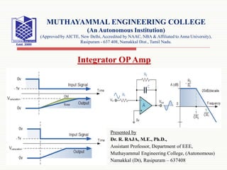
- 1. Presented by Dr. R. RAJA, M.E., Ph.D., Assistant Professor, Department of EEE, Muthayammal Engineering College, (Autonomous) Namakkal (Dt), Rasipuram – 637408 MUTHAYAMMAL ENGINEERING COLLEGE (An Autonomous Institution) (Approved by AICTE, New Delhi, Accredited by NAAC, NBA & Affiliated to Anna University), Rasipuram - 637 408, Namakkal Dist., Tamil Nadu. Integrator OPAmp
- 2. Integrator Op Amp The integrator Op-amp produces an output voltage that is both proportional to the amplitude and duration of the input signal. Operational amplifiers can be used as part of a positive or negative feedback amplifier or as an adder or subtractor type circuit using just pure resistances in both the input and the feedback loop. But what if we where to change the purely resistive ( Rƒ ) feedback element of an inverting amplifier with a frequency dependant complex element that has a reactance, ( X ), such as a Capacitor, C. What would be the effect on the op- amps voltage gain transfer function over its frequency range as a result of this complex impedance. 10/23/2020 2
- 3. Contd.. By replacing this feedback resistance with a capacitor we now have an RC Network connected across the operational amplifiers feedback path producing another type of operational amplifier circuit commonly called an Op-amp Integrator circuit as shown below. As its name implies, the Op-amp Integrator is an operational amplifier circuit that performs the mathematical operation of Integration, that is we can cause the output to respond to changes in the input voltage over time as the op-amp integrator produces an output voltage which is proportional to the integral of the input voltage. 10/23/2020 3
- 4. Contd.. In other words the magnitude of the output signal is determined by the length of time a voltage is present at its input as the current through the feedback loop charges or discharges the capacitor as the required negative feedback occurs through the capacitor. When a step voltage, Vin is firstly applied to the input of an integrating amplifier, the uncharged capacitor C has very little resistance and acts a bit like a short circuit allowing maximum current to flow via the input resistor, Rin as potential difference exists between the two plates. No current flows into the amplifiers input and point X is a virtual earth resulting in zero output. As the impedance of the capacitor at this point is very low, the gain ratio of XC/RIN is also very small giving an overall voltage gain of less than one, ( voltage follower circuit ). As the feedback capacitor, C begins to charge up due to the influence of the input voltage, its impedance Xc slowly increase in proportion to its rate of charge. The capacitor charges up at a rate determined by the RC time constant, ( τ ) of the series RC network. Negative feedback forces the op-amp to produce an output voltage that maintains a virtual earth at the op-amp’s inverting input. 10/23/2020 4
- 5. Contd.. Since the capacitor is connected between the op-amp’s inverting input (which is at virtual ground potential) and the op-amp’s output (which is now negative), the potential voltage, Vc developed across the capacitor slowly increases causing the charging current to decrease as the impedance of the capacitor increases. This results in the ratio of Xc/Rin increasing producing a linearly increasing ramp output voltage that continues to increase until the capacitor is fully charged. At this point the capacitor acts as an open circuit, blocking any more flow of DC current. The ratio of feedback capacitor to input resistor ( XC/RIN ) is now infinite resulting in infinite gain. The result of this high gain (similar to the op- amps open-loop gain), is that the output of the amplifier goes into saturation as shown below. (Saturation occurs when the output voltage of the amplifier swings heavily to one voltage supply rail or the other with little or no control in between). 10/23/2020 5
- 6. Contd.. 10/23/2020 6 The rate at which the output voltage increases (the rate of change) is determined by the value of the resistor and the capacitor, “RC time constant“. By changing this RC time constant value, either by changing the value of the Capacitor, C or the Resistor, R, the time in which it takes the output voltage to reach saturation can also be changed for example.
- 7. Contd.. If we apply a constantly changing input signal such as a square wave to the input of an Integrator Amplifier then the capacitor will charge and discharge in response to changes in the input signal. This results in the output signal being that of a sawtooth waveform whose output is affected by the RC time constant of the resistor/capacitor combination because at higher frequencies, the capacitor has less time to fully charge. This type of circuit is also known as a Ramp Generator and the transfer function is given below. 10/23/2020 7
- 8. Contd.. We know from first principals that the voltage on the plates of a capacitor is equal to the charge on the capacitor divided by its capacitance giving Q/C. Then the voltage across the capacitor is output Vout therefore: -Vout = Q/C. If the capacitor is charging and discharging, the rate of charge of voltage across the capacitor is given as: But dQ/dt is electric current and since the node voltage of the integrating op-amp at its inverting input terminal is zero, X = 0, the input current I(in) flowing through the input resistor, Rin is given as: 10/23/2020 8
- 9. Contd.. The current flowing through the feedback capacitor C is given as: Assuming that the input impedance of the op-amp is infinite (ideal op-amp), no current flows into the op-amp terminal. Therefore, the nodal equation at the inverting input terminal is given as: To simplify the math’s a little, this can also be re-written as: 10/23/2020 9
- 10. Contd.. Where: ω = 2πƒ and the output voltage Vout is a constant 1/RC times the integral of the input voltage VIN with respect to time. Thus the circuit has the transfer function of an inverting integrator with the gain constant of -1/RC. The minus sign ( – ) indicates a 180o phase shift because the input signal is connected directly to the inverting input terminal of the operational amplifier. The AC or Continuous Op-amp Integrator If we changed the above square wave input signal to that of a sine wave of varying frequency the Op-amp Integrator performs less like an integrator and begins to behave more like an active “Low Pass Filter”, passing low frequency signals while attenuating the high frequencies. At zero frequency (0Hz) or DC, the capacitor acts like an open circuit due to its reactance thus blocking any output voltage feedback. As a result very little negative feedback is provided from the output back to the input of the amplifier. 10/23/2020 10
- 11. Contd.. Therefore with just a single capacitor, C in the feedback path, at zero frequency the op-amp is effectively connected as a normal open-loop amplifier with very high open-loop gain. This results in the op-amp becoming unstable cause undesirable output voltage conditions and possible voltage rail saturation. This circuit connects a high value resistance in parallel with a continuously charging and discharging capacitor. The addition of this feedback resistor, R2 across the capacitor, C gives the circuit the characteristics of an inverting amplifier with finite closed-loop voltage gain given by: R2/R1. The result is at high frequencies the capacitor shorts out this feedback resistor, R2 due to the effects of capacitive reactance reducing the amplifiers gain. At normal operating frequencies the circuit acts as an standard integrator, while at very low frequencies approaching 0Hz, when C becomes open-circuited due to its reactance, the magnitude of the voltage gain is limited and controlled by the ratio of: R2/R1. 10/23/2020 11
- 12. Contd.. The AC Op-amp Integrator with DC Gain Control Unlike the DC integrator amplifier above whose output voltage at any instant will be the integral of a waveform so that when the input is a square wave, the output waveform will be triangular. For an AC integrator, a sinusoidal input waveform will produce another sine wave as its output which will be 90o out- of-phase with the input producing a cosine wave. Further more, when the input is triangular, the output waveform is also sinusoidal. This then forms the basis of a Active Low Pass Filter as seen before in the filters section tutorials with a corner frequency given as. 10/23/2020 12
- 13. Contd.. 10/23/2020 13 n the next tutorial about Operational Amplifiers, we will look at another type of operational amplifier circuit which is the opposite or complement of the Op-amp Integrator circuit above called the Differentiator Amplifier. As its name implies, the differentiator amplifier produces an output signal which is the mathematical operation of differentiation, that is it produces a voltage output which is proportional to the input voltage’s rate-of-change and the current flowing through the input capacitor.