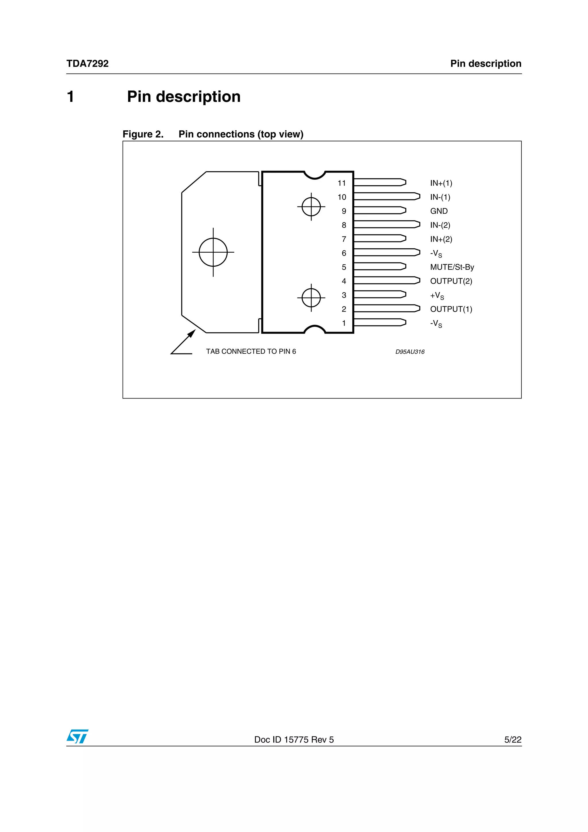
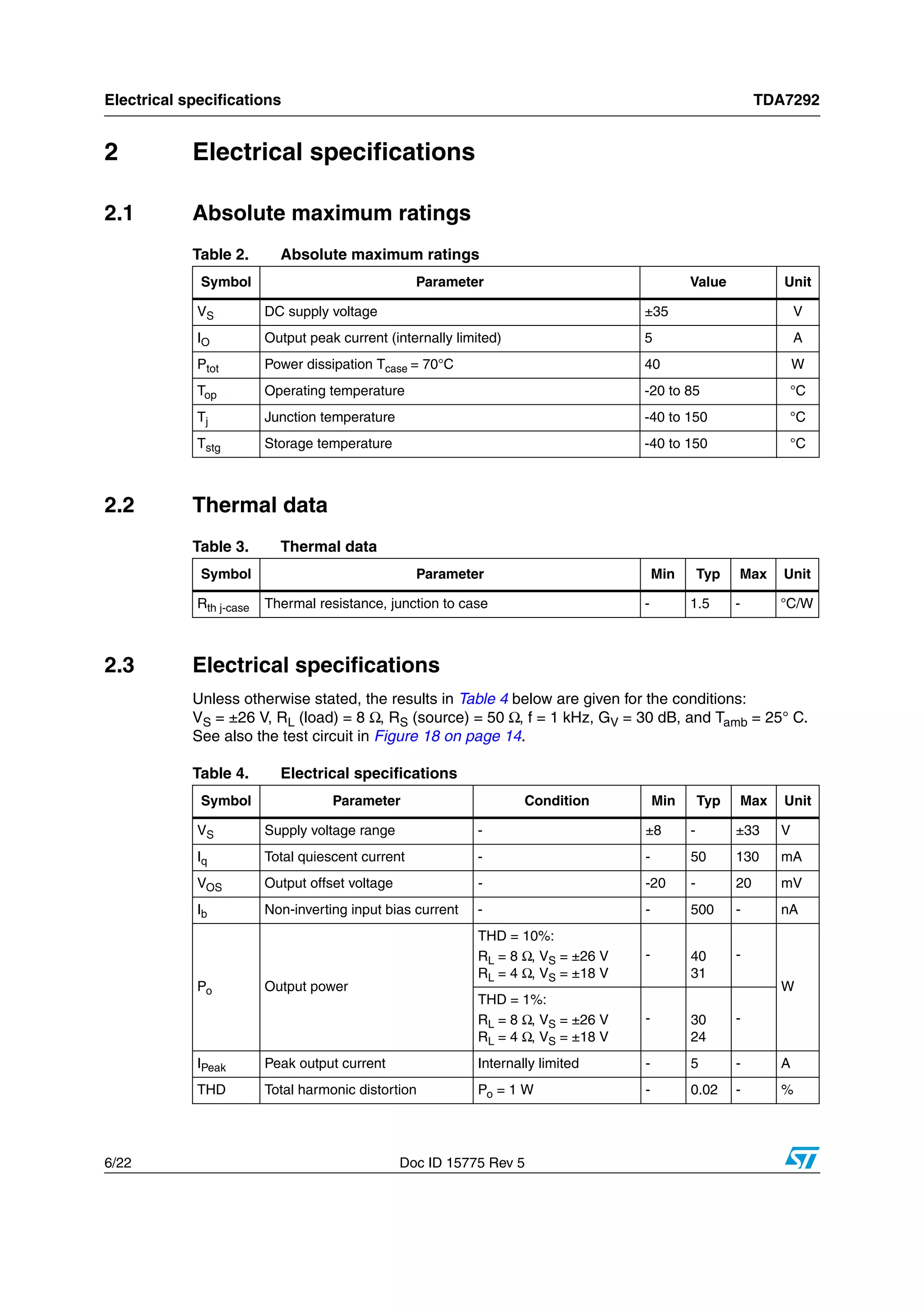
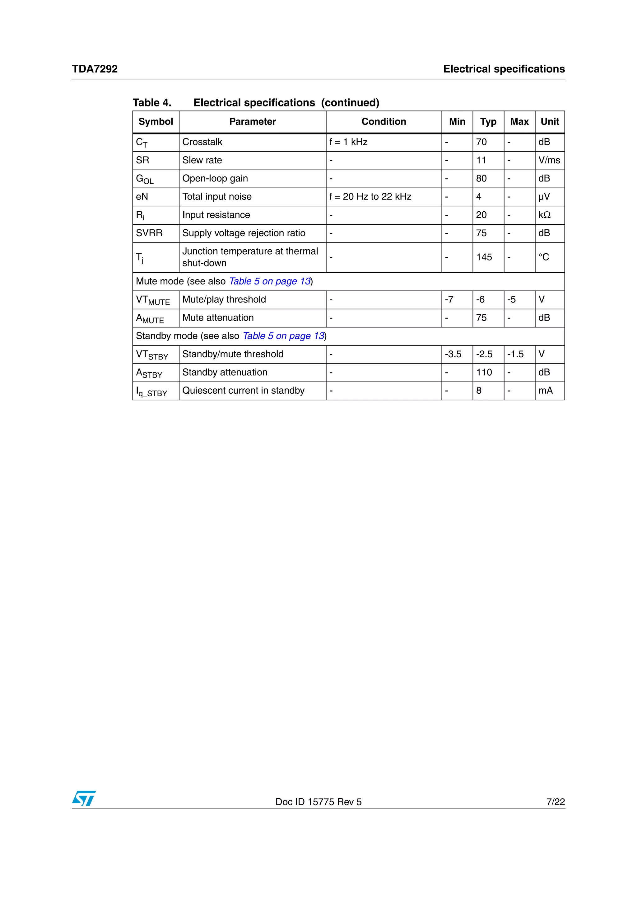
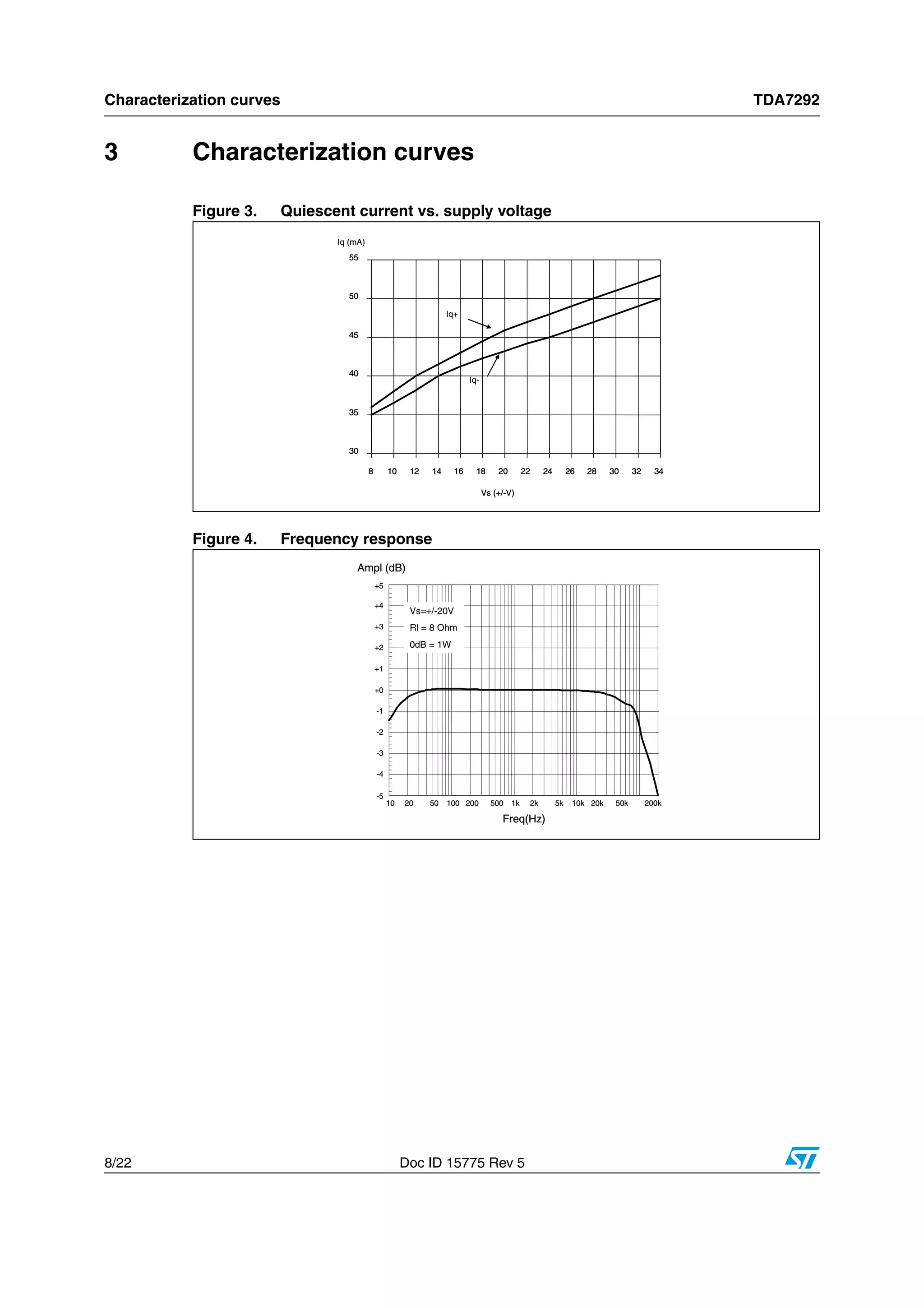
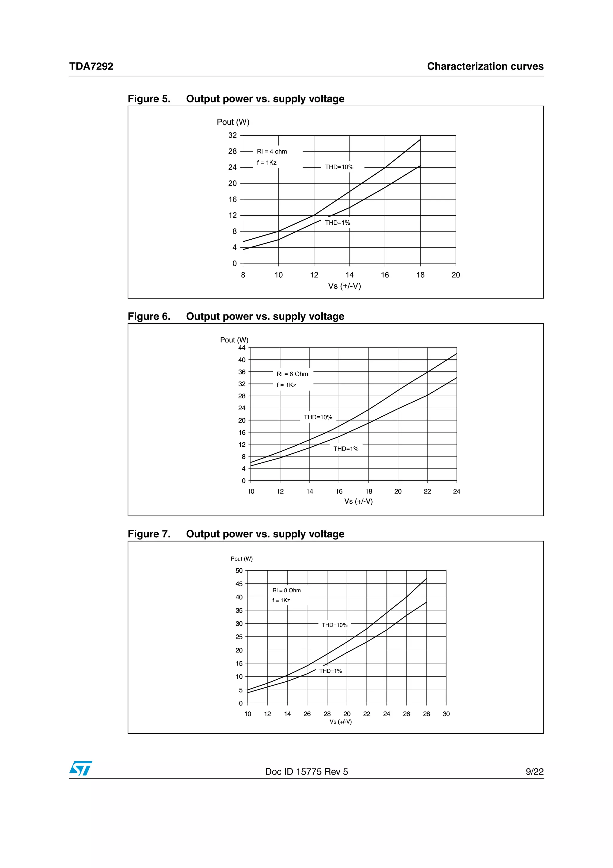
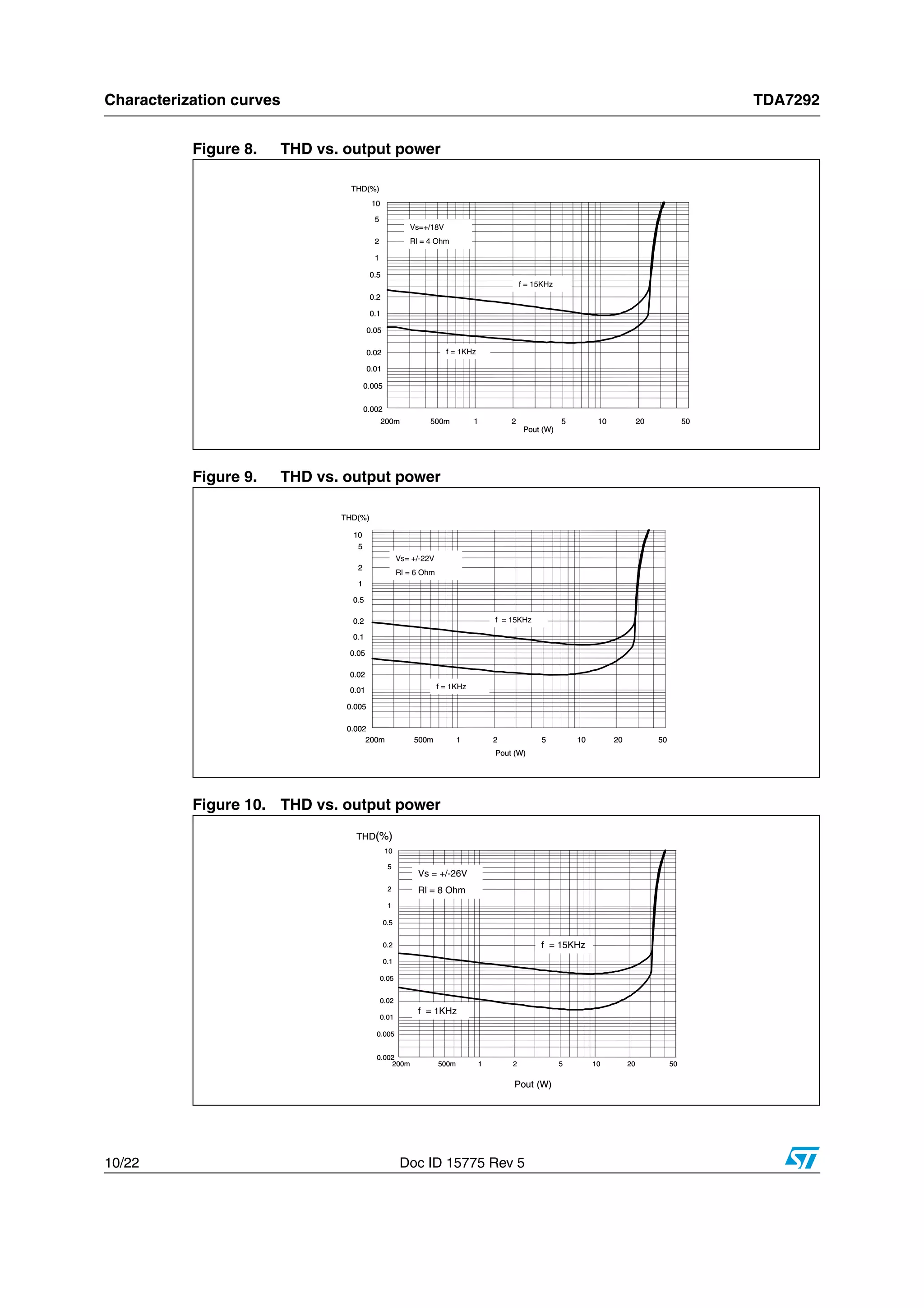
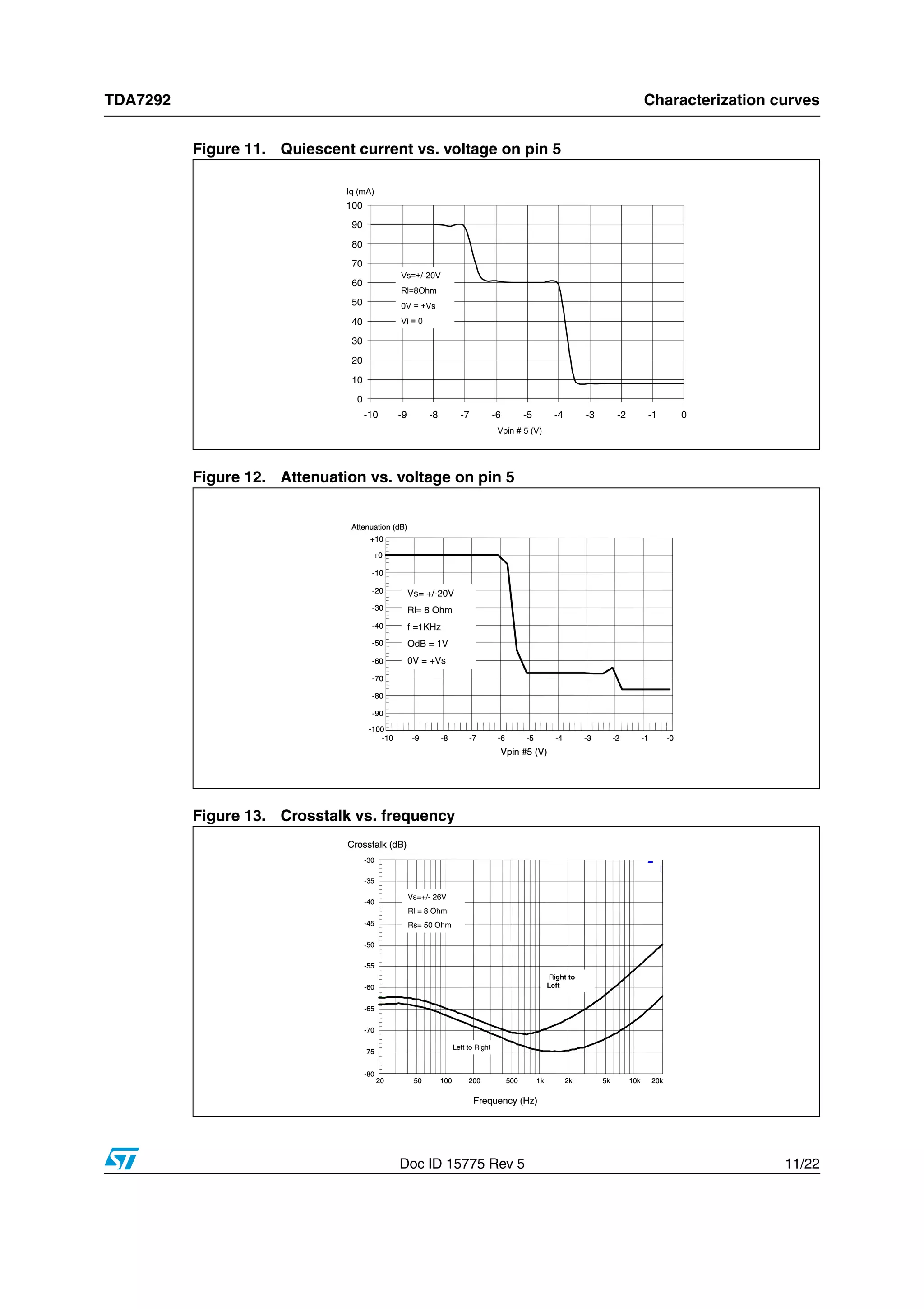
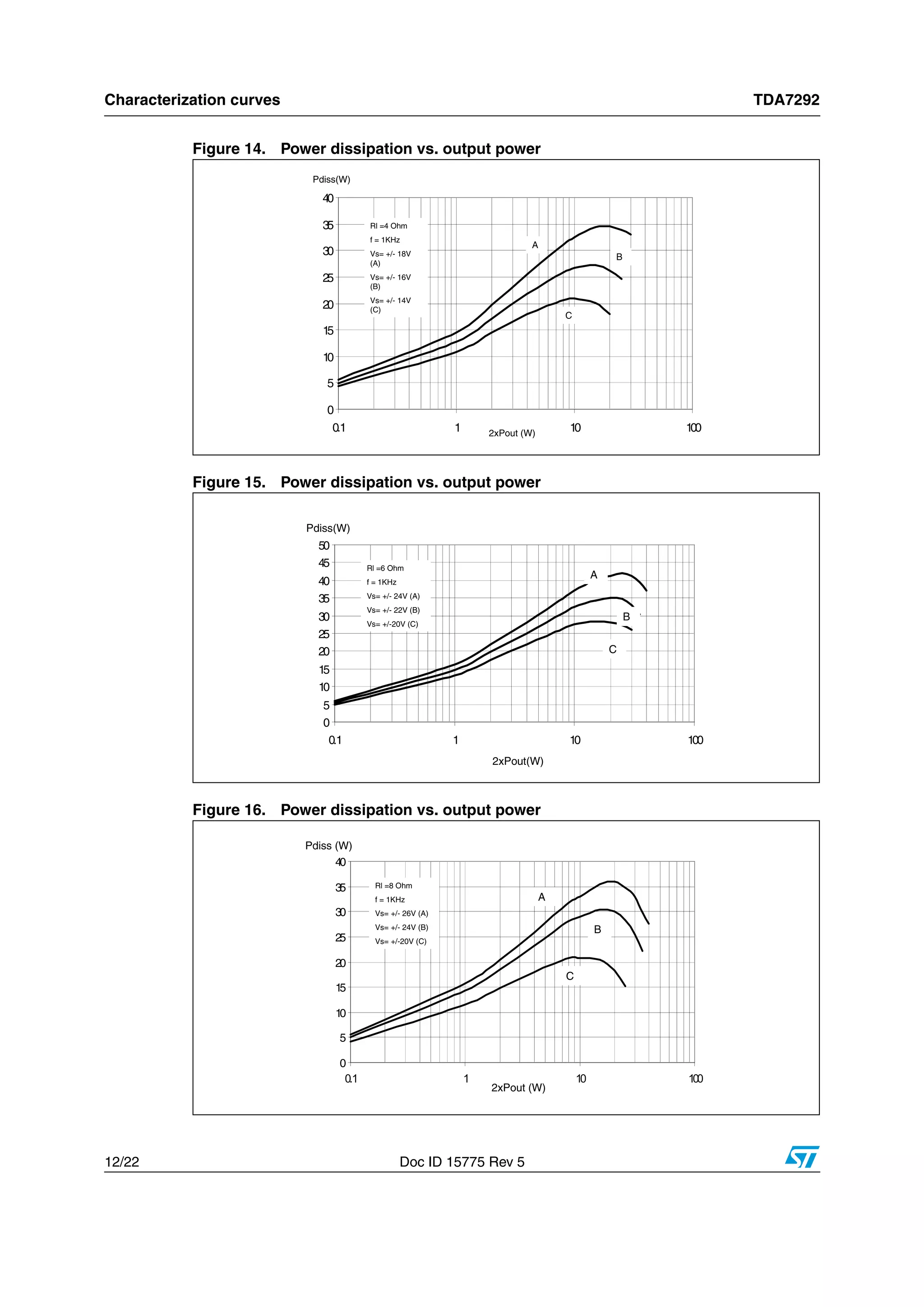
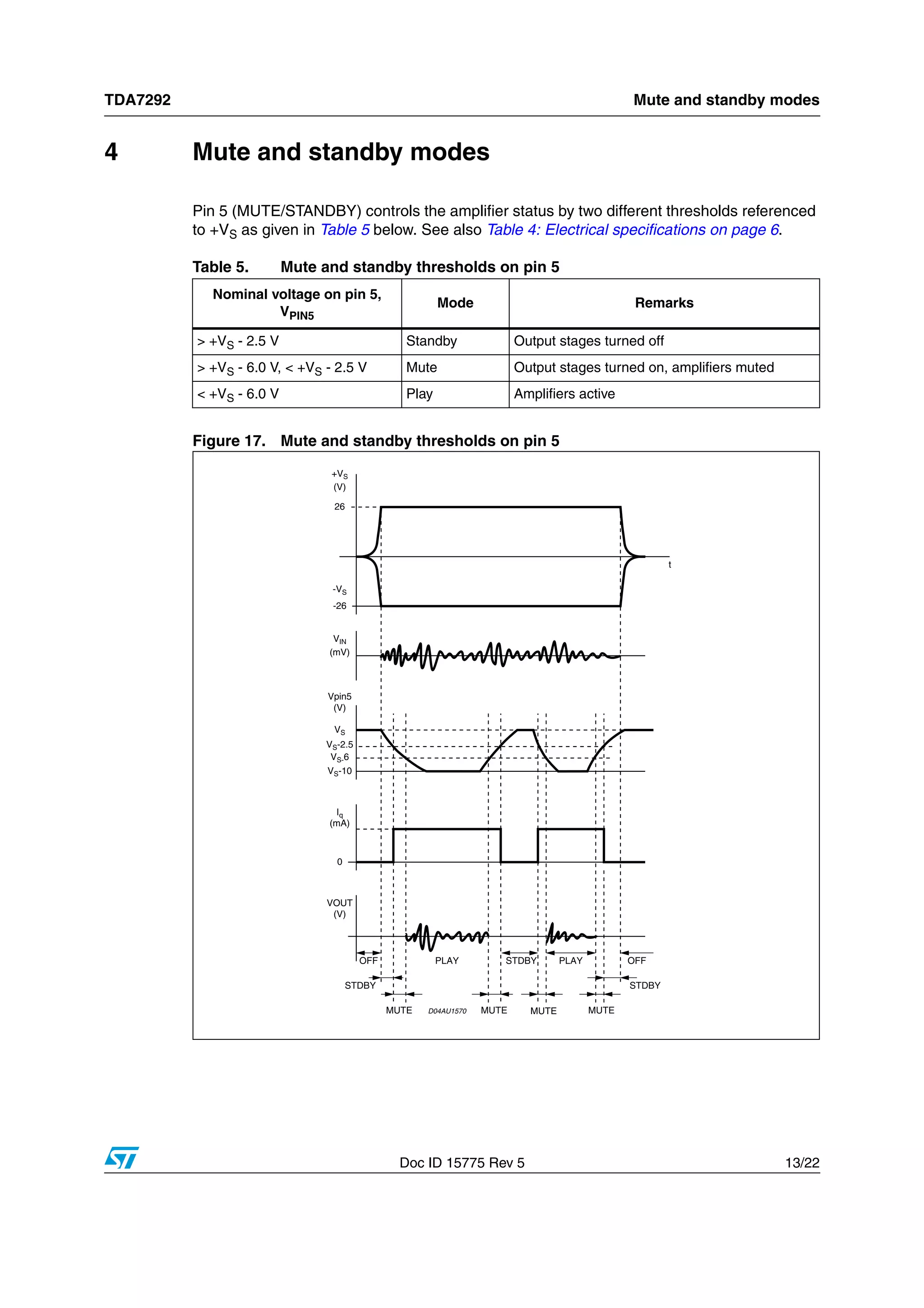
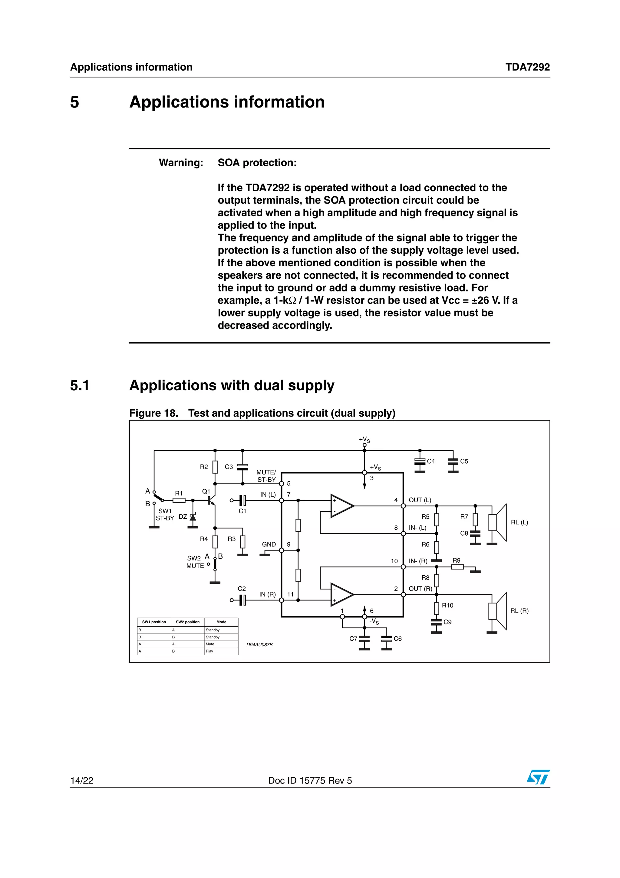
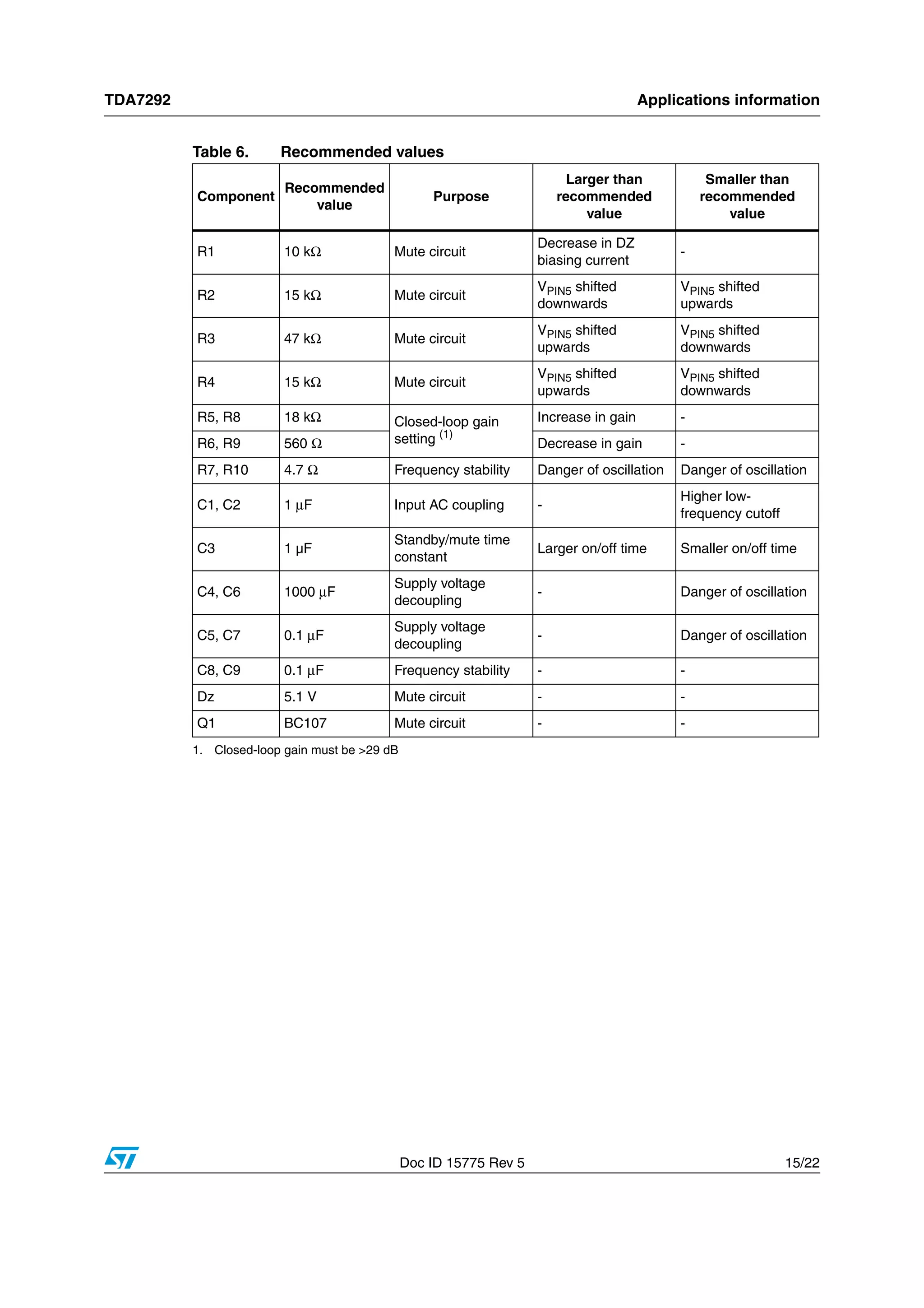
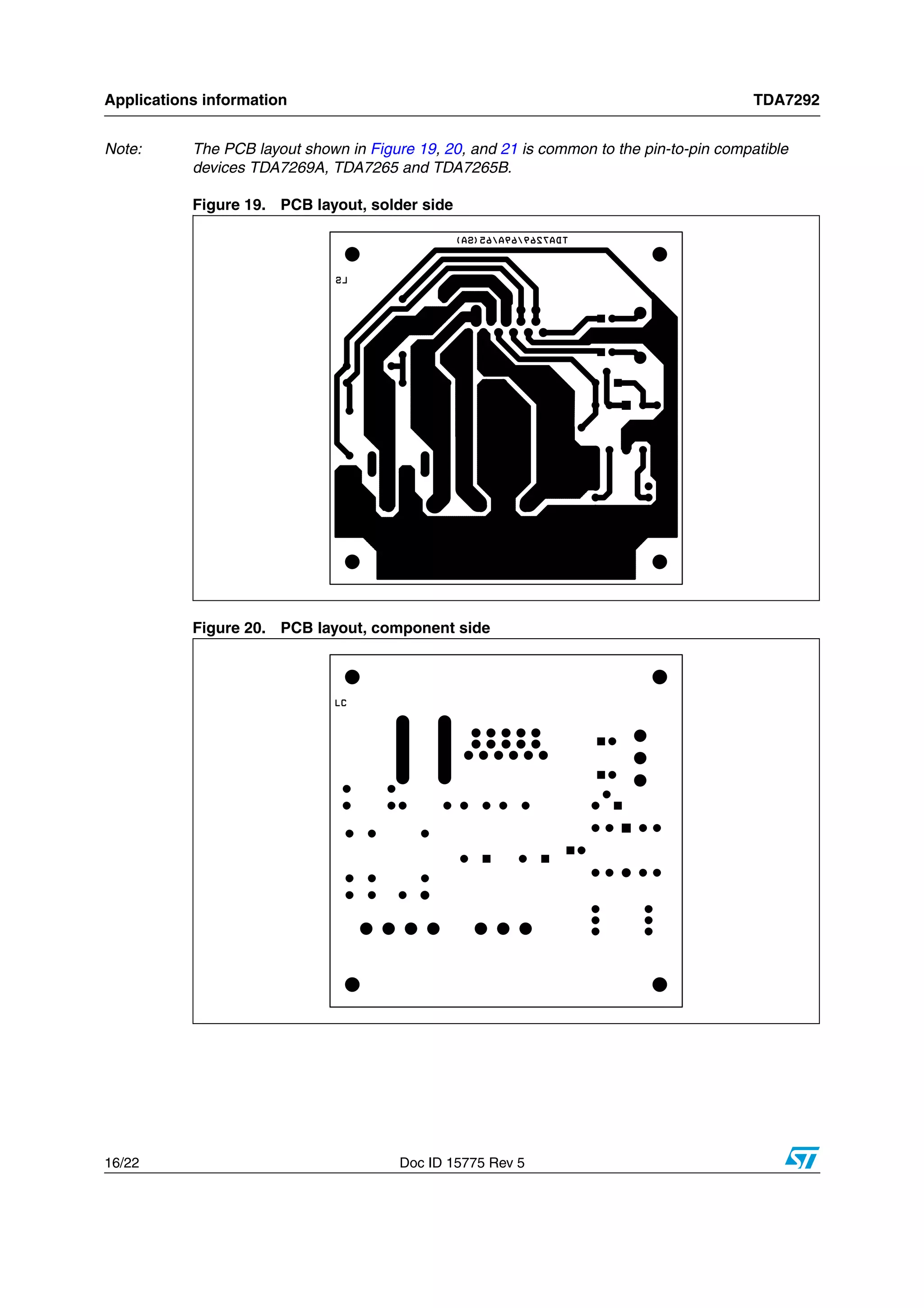
This is information on a product in full production.
February 2012 Doc ID 15775 Rev 5 1/22
1
TDA7292
40 W + 40 W stereo amplifier with mute and standby
Datasheet − production data
Features
■ Wide supply voltage range (up to ± 33 V)
■ Split supply
■ High output power
■ 40 W + 40 W into 8 Ω
with VS = ±26 V and THD = 10%
■ No “pop” at turn on/off
■ Mute (“pop”-free)
■ Standby feature (low Iq)
■ Short-circuit protection
■ Thermal overload protection
Description
The TDA7292 is a class-AB dual audio power
amplifier assembled in a Multiwatt package.
It has been specifically designed for high-quality
sound applications such as hi-fi music centers
and stereo TV sets.
Figure 1. Applications circuit
Multiwatt11
Table 1. Device summary
Order code Operating temp. range Package Packaging
TDA7292 0° to 70° C Multiwatt11 Tube
+5V
18K15K
IN (L)
1μF
15K 1μF
MUTE/
ST-BY
GND
IN (R)
1μF
4.7Ω
4.7Ω
100nF
100nF
OUT (L)
OUT (R)
1000μF
1000μF
+VS
3
5
7
9
6
11
2
4+
+
-
-
D94AU085
RL (L)
RL (R)
-VS
μP
560Ω
18K
IN- (L)8
10 IN- (R)
1
560Ω
18K
47K
www.st.com
Contents TDA7292
2/22 Doc ID 15775 Rev 5
Contents
1 Pin description . . . . . . . . . . . . . . . . . . . . . . . . . . . . . . . . . . . . . . . . . . . . . 5
2 Electrical specifications . . . . . . . . . . . . . . . . . . . . . . . . . . . . . . . . . . . . . . 6
2.1 Absolute maximum ratings . . . . . . . . . . . . . . . . . . . . . . . . . . . . . . . . . . . . . 6
2.2 Thermal data . . . . . . . . . . . . . . . . . . . . . . . . . . . . . . . . . . . . . . . . . . . . . . . 6
2.3 Electrical specifications . . . . . . . . . . . . . . . . . . . . . . . . . . . . . . . . . . . . . . . 6
3 Characterization curves . . . . . . . . . . . . . . . . . . . . . . . . . . . . . . . . . . . . . . 8
4 Mute and standby modes . . . . . . . . . . . . . . . . . . . . . . . . . . . . . . . . . . . . 13
5 Applications information . . . . . . . . . . . . . . . . . . . . . . . . . . . . . . . . . . . . 14
5.1 Applications with dual supply . . . . . . . . . . . . . . . . . . . . . . . . . . . . . . . . . . 14
5.2 Applications with single supply . . . . . . . . . . . . . . . . . . . . . . . . . . . . . . . . . 17
6 Package mechanical data . . . . . . . . . . . . . . . . . . . . . . . . . . . . . . . . . . . . 20
7 Revision history . . . . . . . . . . . . . . . . . . . . . . . . . . . . . . . . . . . . . . . . . . . 21
TDA7292 List of tables
Doc ID 15775 Rev 5 3/22
List of tables
Table 1. Device summary . . . . . . . . . . . . . . . . . . . . . . . . . . . . . . . . . . . . . . . . . . . . . . . . . . . . . . . . . . 1
Table 2. Absolute maximum ratings . . . . . . . . . . . . . . . . . . . . . . . . . . . . . . . . . . . . . . . . . . . . . . . . . . 6
Table 3. Thermal data. . . . . . . . . . . . . . . . . . . . . . . . . . . . . . . . . . . . . . . . . . . . . . . . . . . . . . . . . . . . . 6
Table 4. Electrical specifications. . . . . . . . . . . . . . . . . . . . . . . . . . . . . . . . . . . . . . . . . . . . . . . . . . . . . 6
Table 5. Mute and standby thresholds on pin 5 . . . . . . . . . . . . . . . . . . . . . . . . . . . . . . . . . . . . . . . . 13
Table 6. Recommended values . . . . . . . . . . . . . . . . . . . . . . . . . . . . . . . . . . . . . . . . . . . . . . . . . . . . 15
Table 7. Document revision history . . . . . . . . . . . . . . . . . . . . . . . . . . . . . . . . . . . . . . . . . . . . . . . . . 21
List of figures TDA7292
4/22 Doc ID 15775 Rev 5
List of figures
Figure 1. Applications circuit . . . . . . . . . . . . . . . . . . . . . . . . . . . . . . . . . . . . . . . . . . . . . . . . . . . . . . . . 1
Figure 2. Pin connections (top view) . . . . . . . . . . . . . . . . . . . . . . . . . . . . . . . . . . . . . . . . . . . . . . . . . . 5
Figure 3. Quiescent current vs. supply voltage . . . . . . . . . . . . . . . . . . . . . . . . . . . . . . . . . . . . . . . . . . 8
Figure 4. Frequency response . . . . . . . . . . . . . . . . . . . . . . . . . . . . . . . . . . . . . . . . . . . . . . . . . . . . . . 8
Figure 5. Output power vs. supply voltage . . . . . . . . . . . . . . . . . . . . . . . . . . . . . . . . . . . . . . . . . . . . . 9
Figure 6. Output power vs. supply voltage . . . . . . . . . . . . . . . . . . . . . . . . . . . . . . . . . . . . . . . . . . . . . 9
Figure 7. Output power vs. supply voltage . . . . . . . . . . . . . . . . . . . . . . . . . . . . . . . . . . . . . . . . . . . . . 9
Figure 8. THD vs. output power . . . . . . . . . . . . . . . . . . . . . . . . . . . . . . . . . . . . . . . . . . . . . . . . . . . . 10
Figure 9. THD vs. output power . . . . . . . . . . . . . . . . . . . . . . . . . . . . . . . . . . . . . . . . . . . . . . . . . . . . 10
Figure 10. THD vs. output power . . . . . . . . . . . . . . . . . . . . . . . . . . . . . . . . . . . . . . . . . . . . . . . . . . . . 10
Figure 11. Quiescent current vs. voltage on pin 5 . . . . . . . . . . . . . . . . . . . . . . . . . . . . . . . . . . . . . . . 11
Figure 12. Attenuation vs. voltage on pin 5 . . . . . . . . . . . . . . . . . . . . . . . . . . . . . . . . . . . . . . . . . . . . . 11
Figure 13. Crosstalk vs. frequency . . . . . . . . . . . . . . . . . . . . . . . . . . . . . . . . . . . . . . . . . . . . . . . . . . . 11
Figure 14. Power dissipation vs. output power . . . . . . . . . . . . . . . . . . . . . . . . . . . . . . . . . . . . . . . . . . 12
Figure 15. Power dissipation vs. output power . . . . . . . . . . . . . . . . . . . . . . . . . . . . . . . . . . . . . . . . . . 12
Figure 16. Power dissipation vs. output power . . . . . . . . . . . . . . . . . . . . . . . . . . . . . . . . . . . . . . . . . . 12
Figure 17. Mute and standby thresholds on pin 5 . . . . . . . . . . . . . . . . . . . . . . . . . . . . . . . . . . . . . . . . 13
Figure 18. Test and applications circuit (dual supply) . . . . . . . . . . . . . . . . . . . . . . . . . . . . . . . . . . . . . 14
Figure 19. PCB layout, solder side . . . . . . . . . . . . . . . . . . . . . . . . . . . . . . . . . . . . . . . . . . . . . . . . . . . 16
Figure 20. PCB layout, component side . . . . . . . . . . . . . . . . . . . . . . . . . . . . . . . . . . . . . . . . . . . . . . . 16
Figure 21. PCB component placement . . . . . . . . . . . . . . . . . . . . . . . . . . . . . . . . . . . . . . . . . . . . . . . . 17
Figure 22. Typical applications circuit (single supply) . . . . . . . . . . . . . . . . . . . . . . . . . . . . . . . . . . . . . 17
Figure 23. PCB layout, solder side . . . . . . . . . . . . . . . . . . . . . . . . . . . . . . . . . . . . . . . . . . . . . . . . . . . 18
Figure 24. PCB layout, component side . . . . . . . . . . . . . . . . . . . . . . . . . . . . . . . . . . . . . . . . . . . . . . . 18
Figure 25. PCB component placement . . . . . . . . . . . . . . . . . . . . . . . . . . . . . . . . . . . . . . . . . . . . . . . . 19
Figure 26. Multiwatt11 outline drawing and dimensions . . . . . . . . . . . . . . . . . . . . . . . . . . . . . . . . . . . 20
TDA7292 Pin description
Doc ID 15775 Rev 5 5/22
1 Pin description
Figure 2. Pin connections (top view)
1
2
3
4
5
6
7
9
10
11
8
IN+(1)
IN-(1)
GND
IN-(2)
IN+(2)
-VS
MUTE/St-By
OUTPUT(2)
+VS
OUTPUT(1)
-VS
TAB CONNECTED TO PIN 6 D95AU316
Electrical specifications TDA7292
6/22 Doc ID 15775 Rev 5
2 Electrical specifications
2.1 Absolute maximum ratings
2.2 Thermal data
2.3 Electrical specifications
Unless otherwise stated, the results in Table 4 below are given for the conditions:
VS = ±26 V, RL (load) = 8 Ω, RS (source) = 50 Ω, f = 1 kHz, GV = 30 dB, and Tamb = 25° C.
See also the test circuit in Figure 18 on page 14.
Table 2. Absolute maximum ratings
Symbol Parameter Value Unit
VS DC supply voltage ±35 V
IO Output peak current (internally limited) 5 A
Ptot Power dissipation Tcase = 70°C 40 W
Top Operating temperature -20 to 85 °C
Tj Junction temperature -40 to 150 °C
Tstg Storage temperature -40 to 150 °C
Table 3. Thermal data
Symbol Parameter Min Typ Max Unit
Rth j-case Thermal resistance, junction to case - 1.5 - °C/W
Table 4. Electrical specifications
Symbol Parameter Condition Min Typ Max Unit
VS Supply voltage range - ±8 - ±33 V
Iq Total quiescent current - - 50 130 mA
VOS Output offset voltage - -20 - 20 mV
Ib Non-inverting input bias current - - 500 - nA
Po Output power
THD = 10%:
RL = 8 Ω, VS = ±26 V
RL = 4 Ω, VS = ±18 V
- 40
31
-
W
THD = 1%:
RL = 8 Ω, VS = ±26 V
RL = 4 Ω, VS = ±18 V
- 30
24
-
IPeak Peak output current Internally limited - 5 - A
THD Total harmonic distortion Po = 1 W - 0.02 - %
TDA7292 Electrical specifications
Doc ID 15775 Rev 5 7/22
CT Crosstalk f = 1 kHz - 70 - dB
SR Slew rate - - 11 - V/ms
GOL Open-loop gain - - 80 - dB
eN Total input noise f = 20 Hz to 22 kHz - 4 - µV
Ri Input resistance - - 20 - kΩ
SVRR Supply voltage rejection ratio - - 75 - dB
Tj
Junction temperature at thermal
shut-down
- - 145 - °C
Mute mode (see also Table 5 on page 13)
VTMUTE Mute/play threshold - -7 -6 -5 V
AMUTE Mute attenuation - - 75 - dB
Standby mode (see also Table 5 on page 13)
VTSTBY Standby/mute threshold - -3.5 -2.5 -1.5 V
ASTBY Standby attenuation - - 110 - dB
Iq_STBY Quiescent current in standby - - 8 - mA
Table 4. Electrical specifications (continued)
Symbol Parameter Condition Min Typ Max Unit
Characterization curves TDA7292
8/22 Doc ID 15775 Rev 5
3 Characterization curves
Figure 3. Quiescent current vs. supply voltage
Figure 4. Frequency response
Iq (mA)
Iq+
Iq-
Vs (+/-V)
30
35
40
45
50
55
8 10 12 14 16 18 20 22 24 26 28 30 32 34
Iq (mA)
Iq+
Iq-
Vs (+/-V)
30
35
40
45
50
55
8 10 12 14 16 18 20 22 24 26 28 30 32 34
Iq+
Iq-
Vs (+/-V)
30
35
40
45
50
55
8 10 12 14 16 18 20 22 24 26 28 30 32 34
30
35
40
45
50
55
8 10 12 14 16 18 20 22 24 26 28 30 32 34
-5
+5
-4
-3
-2
-1
+0
+1
+2
+3
+4
10 200k20 50 100 200 500 1k 2k 5k 10k 20k 50k
Vs=+/-20V
Rl = 8 Ohm
0dB = 1W
Freq(Hz)
Ampl (dB)
-5
+5
-4
-3
-2
-1
+0
+1
+2
+3
+4
10 200k20 50 100 200 500 1k 2k 5k 10k 20k 50k
Vs=+/-20V
Rl = 8 Ohm
0dB = 1W
Freq(Hz)
Ampl (dB)
TDA7292 Characterization curves
Doc ID 15775 Rev 5 9/22
Figure 5. Output power vs. supply voltage
Figure 6. Output power vs. supply voltage
Figure 7. Output power vs. supply voltage
0
4
8
12
16
20
24
28
32
8 10 12 14 16 18 20
Pout (W)
Vs (+/-V)
THD=10%
THD=1%
Rl = 4 ohm
f = 1Kz
0
4
8
12
16
20
24
28
32
8 10 12 14 16 18 20
Pout (W)
Vs (+/-V)
THD=10%
THD=1%
Rl = 4 ohm
f = 1Kz
0
4
8
12
16
20
24
28
32
36
40
44
10 12 14 16 18 20 22 24
Pout (W)
Vs (+/-V)
Rl = 6 Ohm
f = 1Kz
THD=1%
THD=10%
0
4
8
12
16
20
24
28
32
36
40
44
10 12 14 16 18 20 22 24
Pout (W)
Vs (+/-V)
Rl = 6 Ohm
f = 1Kz
THD=1%
THD=10%
0
5
10
15
20
25
30
35
40
45
50
10 12 14 26 28 20 22 24 26 28 30
Rl = 8 Ohm
f = 1Kz
Vs (+/-V)
Pout (W)
THD=10%
THD=1%
0
5
10
15
20
25
30
35
40
45
50
10 12 14 26 28 20 22 24 26 28 30
Rl = 8 Ohm
f = 1Kz
Vs (+/-V)
Pout (W)
THD=10%
THD=1%
Characterization curves TDA7292
10/22 Doc ID 15775 Rev 5
Figure 8. THD vs. output power
Figure 9. THD vs. output power
Figure 10. THD vs. output power
0.002
10
0.005
0.01
0.02
0.05
0.1
0.2
0.5
1
2
5
200m 50500m 1 2 5 10 20
THD(%)
Pout (W)
Vs=+/18V
Rl = 4 Ohm
f = 1KHz
f = 15KHz
0.002
10
0.005
0.01
0.02
0.05
0.1
0.2
0.5
1
2
5
200m 50500m 1 2 5 10 20
THD(%)
Pout (W)
Vs=+/18V
Rl = 4 Ohm
f = 1KHz
f = 15KHz
0.002
0.005
0.01
0.02
0.05
0.1
0.2
0.5
1
2
5
200m 50500m 1 2 5 10 20
f = 15KHz
f = 1KHz
Vs= +/-22V
Rl = 6 Ohm
10
THD(%)
Pout (W)
0.002
0.005
0.01
0.02
0.05
0.1
0.2
0.5
1
2
5
200m 50500m 1 2 5 10 20
f = 15KHz
f = 1KHz
Vs= +/-22V
Rl = 6 Ohm
10
THD(%)
Pout (W)
0.002
10
0.005
0.01
0.02
0.05
0.1
0.2
0.5
1
2
5
200m 50500m 1 2 5 10 20
THD(%)
Pout (W)
Vs = +/-26V
Rl = 8 Ohm
f = 1KHz
f = 15KHz
0.002
10
0.005
0.01
0.02
0.05
0.1
0.2
0.5
1
2
5
200m 50500m 1 2 5 10 20
THD(%)
Pout (W)
Vs = +/-26V
Rl = 8 Ohm
f = 1KHz
f = 15KHz
TDA7292 Characterization curves
Doc ID 15775 Rev 5 11/22
Figure 11. Quiescent current vs. voltage on pin 5
Figure 12. Attenuation vs. voltage on pin 5
Figure 13. Crosstalk vs. frequency
0
10
20
30
40
50
60
70
80
90
100
-10 -9 -8 -7 -6 -5 -4 -3 -2 -1 0
Vpin # 5 (V)
Iq (mA)
Vs=+/-20V
Rl=8Ohm
0V = +Vs
Vi = 0
-100
+10
-90
-80
-70
-60
-50
-40
-30
-20
-10
+0
-10 -0-9 -8 -7 -6 -5 -4 -3 -2 -1
Attenuation (dB)
Vpin #5 (V)
Vs= +/-20V
Rl= 8 Ohm
f =1KHz
OdB = 1V
0V = +Vs
-100
+10
-90
-80
-70
-60
-50
-40
-30
-20
-10
+0
-10 -0-9 -8 -7 -6 -5 -4 -3 -2 -1
Attenuation (dB)
Vpin #5 (V)
Vs= +/-20V
Rl= 8 Ohm
f =1KHz
OdB = 1V
0V = +Vs
-80
-30
-75
-70
-65
-60
-55
-50
-45
-40
-35
20 20k50 100 200 500 1k 2k 5k 10k
Vs=+/- 26V
Rl = 8 Ohm
Rs= 50 Ohm
Left to Right
Right to
Left
Crosstalk (dB)
Frequency (Hz)
-80
-30
-75
-70
-65
-60
-55
-50
-45
-40
-35
20 20k50 100 200 500 1k 2k 5k 10k
Vs=+/- 26V
Rl = 8 Ohm
Rs= 50 Ohm
Left to Right
Right to
Left
Crosstalk (dB)
Frequency (Hz)
Characterization curves TDA7292
12/22 Doc ID 15775 Rev 5
Figure 14. Power dissipation vs. output power
Figure 15. Power dissipation vs. output power
Figure 16. Power dissipation vs. output power
0
5
10
15
20
25
30
35
40
0.1 1 10 100
Rl =4 Ohm
f = 1KHz
Vs= +/- 18V
(A)
Vs= +/- 16V
(B)
Vs= +/- 14V
(C)
A
2xPout (W)
Pdiss(W)
B
C
0
5
10
15
20
25
30
35
40
0.1 1 10 100
Rl =4 Ohm
f = 1KHz
Vs= +/- 18V
(A)
Vs= +/- 16V
(B)
Vs= +/- 14V
(C)
A
2xPout (W)
Pdiss(W)
B
C
Rl =4 Ohm
f = 1KHz
Vs= +/- 18V
(A)
Vs= +/- 16V
(B)
Vs= +/- 14V
(C)
A
2xPout (W)
Pdiss(W)
B
C
0
5
10
15
20
25
30
35
40
45
50
0.1 1 10 100
Pdiss(W)
Rl =6 Ohm
f = 1KHz
Vs= +/- 24V (A)
Vs= +/- 22V (B)
Vs= +/-20V (C)
A
B
C
2xPout(W)
0
5
10
15
20
25
30
35
40
45
50
0.1 1 10 100
Pdiss(W)
Rl =6 Ohm
f = 1KHz
Vs= +/- 24V (A)
Vs= +/- 22V (B)
Vs= +/-20V (C)
A
B
C
2xPout(W)
Rl =6 Ohm
f = 1KHz
Vs= +/- 24V (A)
Vs= +/- 22V (B)
Vs= +/-20V (C)
A
B
C
2xPout(W)
0
5
10
15
20
25
30
35
40
0.1 1 10 100
Rl =8 Ohm
f = 1KHz
Vs= +/- 26V (A)
Vs= +/- 24V (B)
Vs= +/-20V (C)
A
B
C
Pdiss (W)
2xPout (W)
Rl =8 Ohm
f = 1KHz
Vs= +/- 26V (A)
Vs= +/- 24V (B)
Vs= +/-20V (C)
A
B
C
Pdiss (W)
2xPout (W)
TDA7292 Mute and standby modes
Doc ID 15775 Rev 5 13/22
4 Mute and standby modes
Pin 5 (MUTE/STANDBY) controls the amplifier status by two different thresholds referenced
to +VS as given in Table 5 below. See also Table 4: Electrical specifications on page 6.
Figure 17. Mute and standby thresholds on pin 5
Table 5. Mute and standby thresholds on pin 5
Nominal voltage on pin 5,
VPIN5
Mode Remarks
> +VS - 2.5 V Standby Output stages turned off
> +VS - 6.0 V, < +VS - 2.5 V Mute Output stages turned on, amplifiers muted
< +VS - 6.0 V Play Amplifiers active
t
OFF
STDBY
MUTE MUTE MUTE MUTE
PLAY STDBY PLAY OFF
STDBY
26
+VS
(V)
-26
-VS
VIN
(mV)
Vpin5
(V)
VS
VS-2.5
VS-6
VS-10
Iq
(mA)
0
VOUT
(V)
D04AU1570
Applications information TDA7292
14/22 Doc ID 15775 Rev 5
5 Applications information
Warning: SOA protection:
If the TDA7292 is operated without a load connected to the
output terminals, the SOA protection circuit could be
activated when a high amplitude and high frequency signal is
applied to the input.
The frequency and amplitude of the signal able to trigger the
protection is a function also of the supply voltage level used.
If the above mentioned condition is possible when the
speakers are not connected, it is recommended to connect
the input to ground or add a dummy resistive load. For
example, a 1-kΩ / 1-W resistor can be used at Vcc = ±26 V. If a
lower supply voltage is used, the resistor value must be
decreased accordingly.
5.1 Applications with dual supply
Figure 18. Test and applications circuit (dual supply)
R3
IN (L)
C1
R2 C3
MUTE/
ST-BY
GND
IN (R)
C2
R7
R10
C8
C9
OUT (L)
OUT (R)
C6
C4
+VS
3
5
7
9
6
11
2
4+
+
-
-
D94AU087B
RL (L)
RL (R)
+VS
-VS
R9
R5
IN- (L)8
10 IN- (R)
1
SW1
R1
DZ
R4
SW2
C7
R8
R6
C5
Q1
ST-BY
MUTE
SW1 position SW2 position Mode
B A Standby
B B Standby
A A Mute
A B Play
A
A B
B
TDA7292 Applications information
Doc ID 15775 Rev 5 15/22
Table 6. Recommended values
Component
Recommended
value
Purpose
Larger than
recommended
value
Smaller than
recommended
value
R1 10 kΩ Mute circuit
Decrease in DZ
biasing current
-
R2 15 kΩ Mute circuit
VPIN5 shifted
downwards
VPIN5 shifted
upwards
R3 47 kΩ Mute circuit
VPIN5 shifted
upwards
VPIN5 shifted
downwards
R4 15 kΩ Mute circuit
VPIN5 shifted
upwards
VPIN5 shifted
downwards
R5, R8 18 kΩ Closed-loop gain
setting (1)
1. Closed-loop gain must be >29 dB
Increase in gain -
R6, R9 560 Ω Decrease in gain -
R7, R10 4.7 Ω Frequency stability Danger of oscillation Danger of oscillation
C1, C2 1 μF Input AC coupling -
Higher low-
frequency cutoff
C3 1 µF
Standby/mute time
constant
Larger on/off time Smaller on/off time
C4, C6 1000 μF
Supply voltage
decoupling
- Danger of oscillation
C5, C7 0.1 μF
Supply voltage
decoupling
- Danger of oscillation
C8, C9 0.1 μF Frequency stability - -
Dz 5.1 V Mute circuit - -
Q1 BC107 Mute circuit - -
Applications information TDA7292
16/22 Doc ID 15775 Rev 5
Note: The PCB layout shown in Figure 19, 20, and 21 is common to the pin-to-pin compatible
devices TDA7269A, TDA7265 and TDA7265B.
Figure 19. PCB layout, solder side
Figure 20. PCB layout, component side
TDA7292 Applications information
Doc ID 15775 Rev 5 17/22
Figure 21. PCB component placement
5.2 Applications with single supply
Figure 22. Typical applications circuit (single supply)
PLAY
5V
R2
15K
IN (L)
C3 1μF
R1
10K
C1
1μF
MUTE
IN (R)
C4 1μF
R8
4.7Ω
R7
1K
C7
0.1μF
OUT (L)
OUT (R)
C5
1000μF
+VS
3
5
7
9
6
11
2
4+
+
-
-
D96AU444A
OUT
(L)
OUT
(R)
GND
R4
30K
IN- (L)8
10
IN- (R)
1
R5
1K
R6
30K
R9
4.7Ω
C9 470μF
C10 470μF
C8
0.1μF
R3
15K
0
MUTE
Q1
BS107
C6
0.1μF
D1 5.1V
C2
100μF
Applications information TDA7292
18/22 Doc ID 15775 Rev 5
Note: The PCB layout shown in Figure 23, 24, and 25 is common to the pin-to-pin compatible
devices TDA7269A, TDA7265, and TDA7265B.
Figure 23. PCB layout, solder side
Figure 24. PCB layout, component side
TDA7292 Applications information
Doc ID 15775 Rev 5 19/22
Figure 25. PCB component placement
Package mechanical data TDA7292
20/22 Doc ID 15775 Rev 5
6 Package mechanical data
The TDA7292 comes in an 11-pin Multiwatt package.
Figure 26. Multiwatt11 outline drawing and dimensions
In order to meet environmental requirements, ST offers these devices in different grades of
ECOPACK®
packages, depending on their level of environmental compliance. ECOPACK®
specifications, grade definitions and product status are available at: www.st.com.
ECOPACK®
is an ST trademark.
OUTLINE AND
MECHANICAL DATA
0016035 H
DIM.
mm inch
MIN. TYP. MAX. MIN. TYP. MAX.
A 5 0.197
B 2.65 0.104
C 1.6 0.063
D 1 0.039
E 0.49 0.55 0.019 0.022
F 0.88 0.95 0.035 0.037
G 1.45 1.7 1.95 0.057 0.067 0.077
G1 16.75 17 17.25 0.659 0.669 0.679
H1 19.6 0.772
H2 20.2 0.795
L 21.9 22.2 22.5 0.862 0.874 0.886
L1 21.7 22.1 22.5 0.854 0.87 0.886
L2 17.4 18.1 0.685 0.713
L3 17.25 17.5 17.75 0.679 0.689 0.699
L4 10.3 10.7 10.9 0.406 0.421 0.429
L7 2.65 2.9 0.104 0.114
M 4.25 4.55 4.85 0.167 0.179 0.191
M1 4.73 5.08 5.43 0.186 0.200 0.214
S 1.9 2.6 0.075 0.102
S1 1.9 2.6 0.075 0.102
Dia1 3.65 3.85 0.144 0.152
Multiwatt11 (Vertical)
TDA7292 Revision history
Doc ID 15775 Rev 5 21/22
7 Revision history
Table 7. Document revision history
Date Revision Changes
Nov-2004 1 Initial release.
Oct-2005 2 Inserted PC board and graphics.
Mar-2006 3 Ouput peak current changed.
29-May-2009 4
Updated resistor value setting mute voltage in Figure 1 on
page 1 and Table 5 on page 13.
29-Feb-2012 5
Added Note: on page 16 and Note: on page 18 concerning PCB
layout for pin-to-pin compatible devices.
TDA7292
22/22 Doc ID 15775 Rev 5
Please Read Carefully:
Information in this document is provided solely in connection with ST products. STMicroelectronics NV and its subsidiaries (“ST”) reserve the
right to make changes, corrections, modifications or improvements, to this document, and the products and services described herein at any
time, without notice.
All ST products are sold pursuant to ST’s terms and conditions of sale.
Purchasers are solely responsible for the choice, selection and use of the ST products and services described herein, and ST assumes no
liability whatsoever relating to the choice, selection or use of the ST products and services described herein.
No license, express or implied, by estoppel or otherwise, to any intellectual property rights is granted under this document. If any part of this
document refers to any third party products or services it shall not be deemed a license grant by ST for the use of such third party products
or services, or any intellectual property contained therein or considered as a warranty covering the use in any manner whatsoever of such
third party products or services or any intellectual property contained therein.
UNLESS OTHERWISE SET FORTH IN ST’S TERMS AND CONDITIONS OF SALE ST DISCLAIMS ANY EXPRESS OR IMPLIED
WARRANTY WITH RESPECT TO THE USE AND/OR SALE OF ST PRODUCTS INCLUDING WITHOUT LIMITATION IMPLIED
WARRANTIES OF MERCHANTABILITY, FITNESS FOR A PARTICULAR PURPOSE (AND THEIR EQUIVALENTS UNDER THE LAWS
OF ANY JURISDICTION), OR INFRINGEMENT OF ANY PATENT, COPYRIGHT OR OTHER INTELLECTUAL PROPERTY RIGHT.
UNLESS EXPRESSLY APPROVED IN WRITING BY TWO AUTHORIZED ST REPRESENTATIVES, ST PRODUCTS ARE NOT
RECOMMENDED, AUTHORIZED OR WARRANTED FOR USE IN MILITARY, AIR CRAFT, SPACE, LIFE SAVING, OR LIFE SUSTAINING
APPLICATIONS, NOR IN PRODUCTS OR SYSTEMS WHERE FAILURE OR MALFUNCTION MAY RESULT IN PERSONAL INJURY,
DEATH, OR SEVERE PROPERTY OR ENVIRONMENTAL DAMAGE. ST PRODUCTS WHICH ARE NOT SPECIFIED AS "AUTOMOTIVE
GRADE" MAY ONLY BE USED IN AUTOMOTIVE APPLICATIONS AT USER’S OWN RISK.
Resale of ST products with provisions different from the statements and/or technical features set forth in this document shall immediately void
any warranty granted by ST for the ST product or service described herein and shall not create or extend in any manner whatsoever, any
liability of ST.
ST and the ST logo are trademarks or registered trademarks of ST in various countries.
Information in this document supersedes and replaces all information previously supplied.
The ST logo is a registered trademark of STMicroelectronics. All other names are the property of their respective owners.
© 2012 STMicroelectronics - All rights reserved
STMicroelectronics group of companies
Australia - Belgium - Brazil - Canada - China - Czech Republic - Finland - France - Germany - Hong Kong - India - Israel - Italy - Japan -
Malaysia - Malta - Morocco - Philippines - Singapore - Spain - Sweden - Switzerland - United Kingdom - United States of America
www.st.com
Mouser Electronics
Authorized Distributor
Click to View Pricing, Inventory, Delivery & Lifecycle Information:
STMicroelectronics:
TDA7292

Original audio amplifier ic tda7292 7292 new st microelectronics

  • 1.
    This is informationon a product in full production. February 2012 Doc ID 15775 Rev 5 1/22 1 TDA7292 40 W + 40 W stereo amplifier with mute and standby Datasheet − production data Features ■ Wide supply voltage range (up to ± 33 V) ■ Split supply ■ High output power ■ 40 W + 40 W into 8 Ω with VS = ±26 V and THD = 10% ■ No “pop” at turn on/off ■ Mute (“pop”-free) ■ Standby feature (low Iq) ■ Short-circuit protection ■ Thermal overload protection Description The TDA7292 is a class-AB dual audio power amplifier assembled in a Multiwatt package. It has been specifically designed for high-quality sound applications such as hi-fi music centers and stereo TV sets. Figure 1. Applications circuit Multiwatt11 Table 1. Device summary Order code Operating temp. range Package Packaging TDA7292 0° to 70° C Multiwatt11 Tube +5V 18K15K IN (L) 1μF 15K 1μF MUTE/ ST-BY GND IN (R) 1μF 4.7Ω 4.7Ω 100nF 100nF OUT (L) OUT (R) 1000μF 1000μF +VS 3 5 7 9 6 11 2 4+ + - - D94AU085 RL (L) RL (R) -VS μP 560Ω 18K IN- (L)8 10 IN- (R) 1 560Ω 18K 47K www.st.com
  • 2.
    Contents TDA7292 2/22 DocID 15775 Rev 5 Contents 1 Pin description . . . . . . . . . . . . . . . . . . . . . . . . . . . . . . . . . . . . . . . . . . . . . 5 2 Electrical specifications . . . . . . . . . . . . . . . . . . . . . . . . . . . . . . . . . . . . . . 6 2.1 Absolute maximum ratings . . . . . . . . . . . . . . . . . . . . . . . . . . . . . . . . . . . . . 6 2.2 Thermal data . . . . . . . . . . . . . . . . . . . . . . . . . . . . . . . . . . . . . . . . . . . . . . . 6 2.3 Electrical specifications . . . . . . . . . . . . . . . . . . . . . . . . . . . . . . . . . . . . . . . 6 3 Characterization curves . . . . . . . . . . . . . . . . . . . . . . . . . . . . . . . . . . . . . . 8 4 Mute and standby modes . . . . . . . . . . . . . . . . . . . . . . . . . . . . . . . . . . . . 13 5 Applications information . . . . . . . . . . . . . . . . . . . . . . . . . . . . . . . . . . . . 14 5.1 Applications with dual supply . . . . . . . . . . . . . . . . . . . . . . . . . . . . . . . . . . 14 5.2 Applications with single supply . . . . . . . . . . . . . . . . . . . . . . . . . . . . . . . . . 17 6 Package mechanical data . . . . . . . . . . . . . . . . . . . . . . . . . . . . . . . . . . . . 20 7 Revision history . . . . . . . . . . . . . . . . . . . . . . . . . . . . . . . . . . . . . . . . . . . 21
  • 3.
    TDA7292 List oftables Doc ID 15775 Rev 5 3/22 List of tables Table 1. Device summary . . . . . . . . . . . . . . . . . . . . . . . . . . . . . . . . . . . . . . . . . . . . . . . . . . . . . . . . . . 1 Table 2. Absolute maximum ratings . . . . . . . . . . . . . . . . . . . . . . . . . . . . . . . . . . . . . . . . . . . . . . . . . . 6 Table 3. Thermal data. . . . . . . . . . . . . . . . . . . . . . . . . . . . . . . . . . . . . . . . . . . . . . . . . . . . . . . . . . . . . 6 Table 4. Electrical specifications. . . . . . . . . . . . . . . . . . . . . . . . . . . . . . . . . . . . . . . . . . . . . . . . . . . . . 6 Table 5. Mute and standby thresholds on pin 5 . . . . . . . . . . . . . . . . . . . . . . . . . . . . . . . . . . . . . . . . 13 Table 6. Recommended values . . . . . . . . . . . . . . . . . . . . . . . . . . . . . . . . . . . . . . . . . . . . . . . . . . . . 15 Table 7. Document revision history . . . . . . . . . . . . . . . . . . . . . . . . . . . . . . . . . . . . . . . . . . . . . . . . . 21
  • 4.
    List of figuresTDA7292 4/22 Doc ID 15775 Rev 5 List of figures Figure 1. Applications circuit . . . . . . . . . . . . . . . . . . . . . . . . . . . . . . . . . . . . . . . . . . . . . . . . . . . . . . . . 1 Figure 2. Pin connections (top view) . . . . . . . . . . . . . . . . . . . . . . . . . . . . . . . . . . . . . . . . . . . . . . . . . . 5 Figure 3. Quiescent current vs. supply voltage . . . . . . . . . . . . . . . . . . . . . . . . . . . . . . . . . . . . . . . . . . 8 Figure 4. Frequency response . . . . . . . . . . . . . . . . . . . . . . . . . . . . . . . . . . . . . . . . . . . . . . . . . . . . . . 8 Figure 5. Output power vs. supply voltage . . . . . . . . . . . . . . . . . . . . . . . . . . . . . . . . . . . . . . . . . . . . . 9 Figure 6. Output power vs. supply voltage . . . . . . . . . . . . . . . . . . . . . . . . . . . . . . . . . . . . . . . . . . . . . 9 Figure 7. Output power vs. supply voltage . . . . . . . . . . . . . . . . . . . . . . . . . . . . . . . . . . . . . . . . . . . . . 9 Figure 8. THD vs. output power . . . . . . . . . . . . . . . . . . . . . . . . . . . . . . . . . . . . . . . . . . . . . . . . . . . . 10 Figure 9. THD vs. output power . . . . . . . . . . . . . . . . . . . . . . . . . . . . . . . . . . . . . . . . . . . . . . . . . . . . 10 Figure 10. THD vs. output power . . . . . . . . . . . . . . . . . . . . . . . . . . . . . . . . . . . . . . . . . . . . . . . . . . . . 10 Figure 11. Quiescent current vs. voltage on pin 5 . . . . . . . . . . . . . . . . . . . . . . . . . . . . . . . . . . . . . . . 11 Figure 12. Attenuation vs. voltage on pin 5 . . . . . . . . . . . . . . . . . . . . . . . . . . . . . . . . . . . . . . . . . . . . . 11 Figure 13. Crosstalk vs. frequency . . . . . . . . . . . . . . . . . . . . . . . . . . . . . . . . . . . . . . . . . . . . . . . . . . . 11 Figure 14. Power dissipation vs. output power . . . . . . . . . . . . . . . . . . . . . . . . . . . . . . . . . . . . . . . . . . 12 Figure 15. Power dissipation vs. output power . . . . . . . . . . . . . . . . . . . . . . . . . . . . . . . . . . . . . . . . . . 12 Figure 16. Power dissipation vs. output power . . . . . . . . . . . . . . . . . . . . . . . . . . . . . . . . . . . . . . . . . . 12 Figure 17. Mute and standby thresholds on pin 5 . . . . . . . . . . . . . . . . . . . . . . . . . . . . . . . . . . . . . . . . 13 Figure 18. Test and applications circuit (dual supply) . . . . . . . . . . . . . . . . . . . . . . . . . . . . . . . . . . . . . 14 Figure 19. PCB layout, solder side . . . . . . . . . . . . . . . . . . . . . . . . . . . . . . . . . . . . . . . . . . . . . . . . . . . 16 Figure 20. PCB layout, component side . . . . . . . . . . . . . . . . . . . . . . . . . . . . . . . . . . . . . . . . . . . . . . . 16 Figure 21. PCB component placement . . . . . . . . . . . . . . . . . . . . . . . . . . . . . . . . . . . . . . . . . . . . . . . . 17 Figure 22. Typical applications circuit (single supply) . . . . . . . . . . . . . . . . . . . . . . . . . . . . . . . . . . . . . 17 Figure 23. PCB layout, solder side . . . . . . . . . . . . . . . . . . . . . . . . . . . . . . . . . . . . . . . . . . . . . . . . . . . 18 Figure 24. PCB layout, component side . . . . . . . . . . . . . . . . . . . . . . . . . . . . . . . . . . . . . . . . . . . . . . . 18 Figure 25. PCB component placement . . . . . . . . . . . . . . . . . . . . . . . . . . . . . . . . . . . . . . . . . . . . . . . . 19 Figure 26. Multiwatt11 outline drawing and dimensions . . . . . . . . . . . . . . . . . . . . . . . . . . . . . . . . . . . 20
  • 5.
    TDA7292 Pin description DocID 15775 Rev 5 5/22 1 Pin description Figure 2. Pin connections (top view) 1 2 3 4 5 6 7 9 10 11 8 IN+(1) IN-(1) GND IN-(2) IN+(2) -VS MUTE/St-By OUTPUT(2) +VS OUTPUT(1) -VS TAB CONNECTED TO PIN 6 D95AU316
  • 6.
    Electrical specifications TDA7292 6/22Doc ID 15775 Rev 5 2 Electrical specifications 2.1 Absolute maximum ratings 2.2 Thermal data 2.3 Electrical specifications Unless otherwise stated, the results in Table 4 below are given for the conditions: VS = ±26 V, RL (load) = 8 Ω, RS (source) = 50 Ω, f = 1 kHz, GV = 30 dB, and Tamb = 25° C. See also the test circuit in Figure 18 on page 14. Table 2. Absolute maximum ratings Symbol Parameter Value Unit VS DC supply voltage ±35 V IO Output peak current (internally limited) 5 A Ptot Power dissipation Tcase = 70°C 40 W Top Operating temperature -20 to 85 °C Tj Junction temperature -40 to 150 °C Tstg Storage temperature -40 to 150 °C Table 3. Thermal data Symbol Parameter Min Typ Max Unit Rth j-case Thermal resistance, junction to case - 1.5 - °C/W Table 4. Electrical specifications Symbol Parameter Condition Min Typ Max Unit VS Supply voltage range - ±8 - ±33 V Iq Total quiescent current - - 50 130 mA VOS Output offset voltage - -20 - 20 mV Ib Non-inverting input bias current - - 500 - nA Po Output power THD = 10%: RL = 8 Ω, VS = ±26 V RL = 4 Ω, VS = ±18 V - 40 31 - W THD = 1%: RL = 8 Ω, VS = ±26 V RL = 4 Ω, VS = ±18 V - 30 24 - IPeak Peak output current Internally limited - 5 - A THD Total harmonic distortion Po = 1 W - 0.02 - %
  • 7.
    TDA7292 Electrical specifications DocID 15775 Rev 5 7/22 CT Crosstalk f = 1 kHz - 70 - dB SR Slew rate - - 11 - V/ms GOL Open-loop gain - - 80 - dB eN Total input noise f = 20 Hz to 22 kHz - 4 - µV Ri Input resistance - - 20 - kΩ SVRR Supply voltage rejection ratio - - 75 - dB Tj Junction temperature at thermal shut-down - - 145 - °C Mute mode (see also Table 5 on page 13) VTMUTE Mute/play threshold - -7 -6 -5 V AMUTE Mute attenuation - - 75 - dB Standby mode (see also Table 5 on page 13) VTSTBY Standby/mute threshold - -3.5 -2.5 -1.5 V ASTBY Standby attenuation - - 110 - dB Iq_STBY Quiescent current in standby - - 8 - mA Table 4. Electrical specifications (continued) Symbol Parameter Condition Min Typ Max Unit
  • 8.
    Characterization curves TDA7292 8/22Doc ID 15775 Rev 5 3 Characterization curves Figure 3. Quiescent current vs. supply voltage Figure 4. Frequency response Iq (mA) Iq+ Iq- Vs (+/-V) 30 35 40 45 50 55 8 10 12 14 16 18 20 22 24 26 28 30 32 34 Iq (mA) Iq+ Iq- Vs (+/-V) 30 35 40 45 50 55 8 10 12 14 16 18 20 22 24 26 28 30 32 34 Iq+ Iq- Vs (+/-V) 30 35 40 45 50 55 8 10 12 14 16 18 20 22 24 26 28 30 32 34 30 35 40 45 50 55 8 10 12 14 16 18 20 22 24 26 28 30 32 34 -5 +5 -4 -3 -2 -1 +0 +1 +2 +3 +4 10 200k20 50 100 200 500 1k 2k 5k 10k 20k 50k Vs=+/-20V Rl = 8 Ohm 0dB = 1W Freq(Hz) Ampl (dB) -5 +5 -4 -3 -2 -1 +0 +1 +2 +3 +4 10 200k20 50 100 200 500 1k 2k 5k 10k 20k 50k Vs=+/-20V Rl = 8 Ohm 0dB = 1W Freq(Hz) Ampl (dB)
  • 9.
    TDA7292 Characterization curves DocID 15775 Rev 5 9/22 Figure 5. Output power vs. supply voltage Figure 6. Output power vs. supply voltage Figure 7. Output power vs. supply voltage 0 4 8 12 16 20 24 28 32 8 10 12 14 16 18 20 Pout (W) Vs (+/-V) THD=10% THD=1% Rl = 4 ohm f = 1Kz 0 4 8 12 16 20 24 28 32 8 10 12 14 16 18 20 Pout (W) Vs (+/-V) THD=10% THD=1% Rl = 4 ohm f = 1Kz 0 4 8 12 16 20 24 28 32 36 40 44 10 12 14 16 18 20 22 24 Pout (W) Vs (+/-V) Rl = 6 Ohm f = 1Kz THD=1% THD=10% 0 4 8 12 16 20 24 28 32 36 40 44 10 12 14 16 18 20 22 24 Pout (W) Vs (+/-V) Rl = 6 Ohm f = 1Kz THD=1% THD=10% 0 5 10 15 20 25 30 35 40 45 50 10 12 14 26 28 20 22 24 26 28 30 Rl = 8 Ohm f = 1Kz Vs (+/-V) Pout (W) THD=10% THD=1% 0 5 10 15 20 25 30 35 40 45 50 10 12 14 26 28 20 22 24 26 28 30 Rl = 8 Ohm f = 1Kz Vs (+/-V) Pout (W) THD=10% THD=1%
  • 10.
    Characterization curves TDA7292 10/22Doc ID 15775 Rev 5 Figure 8. THD vs. output power Figure 9. THD vs. output power Figure 10. THD vs. output power 0.002 10 0.005 0.01 0.02 0.05 0.1 0.2 0.5 1 2 5 200m 50500m 1 2 5 10 20 THD(%) Pout (W) Vs=+/18V Rl = 4 Ohm f = 1KHz f = 15KHz 0.002 10 0.005 0.01 0.02 0.05 0.1 0.2 0.5 1 2 5 200m 50500m 1 2 5 10 20 THD(%) Pout (W) Vs=+/18V Rl = 4 Ohm f = 1KHz f = 15KHz 0.002 0.005 0.01 0.02 0.05 0.1 0.2 0.5 1 2 5 200m 50500m 1 2 5 10 20 f = 15KHz f = 1KHz Vs= +/-22V Rl = 6 Ohm 10 THD(%) Pout (W) 0.002 0.005 0.01 0.02 0.05 0.1 0.2 0.5 1 2 5 200m 50500m 1 2 5 10 20 f = 15KHz f = 1KHz Vs= +/-22V Rl = 6 Ohm 10 THD(%) Pout (W) 0.002 10 0.005 0.01 0.02 0.05 0.1 0.2 0.5 1 2 5 200m 50500m 1 2 5 10 20 THD(%) Pout (W) Vs = +/-26V Rl = 8 Ohm f = 1KHz f = 15KHz 0.002 10 0.005 0.01 0.02 0.05 0.1 0.2 0.5 1 2 5 200m 50500m 1 2 5 10 20 THD(%) Pout (W) Vs = +/-26V Rl = 8 Ohm f = 1KHz f = 15KHz
  • 11.
    TDA7292 Characterization curves DocID 15775 Rev 5 11/22 Figure 11. Quiescent current vs. voltage on pin 5 Figure 12. Attenuation vs. voltage on pin 5 Figure 13. Crosstalk vs. frequency 0 10 20 30 40 50 60 70 80 90 100 -10 -9 -8 -7 -6 -5 -4 -3 -2 -1 0 Vpin # 5 (V) Iq (mA) Vs=+/-20V Rl=8Ohm 0V = +Vs Vi = 0 -100 +10 -90 -80 -70 -60 -50 -40 -30 -20 -10 +0 -10 -0-9 -8 -7 -6 -5 -4 -3 -2 -1 Attenuation (dB) Vpin #5 (V) Vs= +/-20V Rl= 8 Ohm f =1KHz OdB = 1V 0V = +Vs -100 +10 -90 -80 -70 -60 -50 -40 -30 -20 -10 +0 -10 -0-9 -8 -7 -6 -5 -4 -3 -2 -1 Attenuation (dB) Vpin #5 (V) Vs= +/-20V Rl= 8 Ohm f =1KHz OdB = 1V 0V = +Vs -80 -30 -75 -70 -65 -60 -55 -50 -45 -40 -35 20 20k50 100 200 500 1k 2k 5k 10k Vs=+/- 26V Rl = 8 Ohm Rs= 50 Ohm Left to Right Right to Left Crosstalk (dB) Frequency (Hz) -80 -30 -75 -70 -65 -60 -55 -50 -45 -40 -35 20 20k50 100 200 500 1k 2k 5k 10k Vs=+/- 26V Rl = 8 Ohm Rs= 50 Ohm Left to Right Right to Left Crosstalk (dB) Frequency (Hz)
  • 12.
    Characterization curves TDA7292 12/22Doc ID 15775 Rev 5 Figure 14. Power dissipation vs. output power Figure 15. Power dissipation vs. output power Figure 16. Power dissipation vs. output power 0 5 10 15 20 25 30 35 40 0.1 1 10 100 Rl =4 Ohm f = 1KHz Vs= +/- 18V (A) Vs= +/- 16V (B) Vs= +/- 14V (C) A 2xPout (W) Pdiss(W) B C 0 5 10 15 20 25 30 35 40 0.1 1 10 100 Rl =4 Ohm f = 1KHz Vs= +/- 18V (A) Vs= +/- 16V (B) Vs= +/- 14V (C) A 2xPout (W) Pdiss(W) B C Rl =4 Ohm f = 1KHz Vs= +/- 18V (A) Vs= +/- 16V (B) Vs= +/- 14V (C) A 2xPout (W) Pdiss(W) B C 0 5 10 15 20 25 30 35 40 45 50 0.1 1 10 100 Pdiss(W) Rl =6 Ohm f = 1KHz Vs= +/- 24V (A) Vs= +/- 22V (B) Vs= +/-20V (C) A B C 2xPout(W) 0 5 10 15 20 25 30 35 40 45 50 0.1 1 10 100 Pdiss(W) Rl =6 Ohm f = 1KHz Vs= +/- 24V (A) Vs= +/- 22V (B) Vs= +/-20V (C) A B C 2xPout(W) Rl =6 Ohm f = 1KHz Vs= +/- 24V (A) Vs= +/- 22V (B) Vs= +/-20V (C) A B C 2xPout(W) 0 5 10 15 20 25 30 35 40 0.1 1 10 100 Rl =8 Ohm f = 1KHz Vs= +/- 26V (A) Vs= +/- 24V (B) Vs= +/-20V (C) A B C Pdiss (W) 2xPout (W) Rl =8 Ohm f = 1KHz Vs= +/- 26V (A) Vs= +/- 24V (B) Vs= +/-20V (C) A B C Pdiss (W) 2xPout (W)
  • 13.
    TDA7292 Mute andstandby modes Doc ID 15775 Rev 5 13/22 4 Mute and standby modes Pin 5 (MUTE/STANDBY) controls the amplifier status by two different thresholds referenced to +VS as given in Table 5 below. See also Table 4: Electrical specifications on page 6. Figure 17. Mute and standby thresholds on pin 5 Table 5. Mute and standby thresholds on pin 5 Nominal voltage on pin 5, VPIN5 Mode Remarks > +VS - 2.5 V Standby Output stages turned off > +VS - 6.0 V, < +VS - 2.5 V Mute Output stages turned on, amplifiers muted < +VS - 6.0 V Play Amplifiers active t OFF STDBY MUTE MUTE MUTE MUTE PLAY STDBY PLAY OFF STDBY 26 +VS (V) -26 -VS VIN (mV) Vpin5 (V) VS VS-2.5 VS-6 VS-10 Iq (mA) 0 VOUT (V) D04AU1570
  • 14.
    Applications information TDA7292 14/22Doc ID 15775 Rev 5 5 Applications information Warning: SOA protection: If the TDA7292 is operated without a load connected to the output terminals, the SOA protection circuit could be activated when a high amplitude and high frequency signal is applied to the input. The frequency and amplitude of the signal able to trigger the protection is a function also of the supply voltage level used. If the above mentioned condition is possible when the speakers are not connected, it is recommended to connect the input to ground or add a dummy resistive load. For example, a 1-kΩ / 1-W resistor can be used at Vcc = ±26 V. If a lower supply voltage is used, the resistor value must be decreased accordingly. 5.1 Applications with dual supply Figure 18. Test and applications circuit (dual supply) R3 IN (L) C1 R2 C3 MUTE/ ST-BY GND IN (R) C2 R7 R10 C8 C9 OUT (L) OUT (R) C6 C4 +VS 3 5 7 9 6 11 2 4+ + - - D94AU087B RL (L) RL (R) +VS -VS R9 R5 IN- (L)8 10 IN- (R) 1 SW1 R1 DZ R4 SW2 C7 R8 R6 C5 Q1 ST-BY MUTE SW1 position SW2 position Mode B A Standby B B Standby A A Mute A B Play A A B B
  • 15.
    TDA7292 Applications information DocID 15775 Rev 5 15/22 Table 6. Recommended values Component Recommended value Purpose Larger than recommended value Smaller than recommended value R1 10 kΩ Mute circuit Decrease in DZ biasing current - R2 15 kΩ Mute circuit VPIN5 shifted downwards VPIN5 shifted upwards R3 47 kΩ Mute circuit VPIN5 shifted upwards VPIN5 shifted downwards R4 15 kΩ Mute circuit VPIN5 shifted upwards VPIN5 shifted downwards R5, R8 18 kΩ Closed-loop gain setting (1) 1. Closed-loop gain must be >29 dB Increase in gain - R6, R9 560 Ω Decrease in gain - R7, R10 4.7 Ω Frequency stability Danger of oscillation Danger of oscillation C1, C2 1 μF Input AC coupling - Higher low- frequency cutoff C3 1 µF Standby/mute time constant Larger on/off time Smaller on/off time C4, C6 1000 μF Supply voltage decoupling - Danger of oscillation C5, C7 0.1 μF Supply voltage decoupling - Danger of oscillation C8, C9 0.1 μF Frequency stability - - Dz 5.1 V Mute circuit - - Q1 BC107 Mute circuit - -
  • 16.
    Applications information TDA7292 16/22Doc ID 15775 Rev 5 Note: The PCB layout shown in Figure 19, 20, and 21 is common to the pin-to-pin compatible devices TDA7269A, TDA7265 and TDA7265B. Figure 19. PCB layout, solder side Figure 20. PCB layout, component side
  • 17.
    TDA7292 Applications information DocID 15775 Rev 5 17/22 Figure 21. PCB component placement 5.2 Applications with single supply Figure 22. Typical applications circuit (single supply) PLAY 5V R2 15K IN (L) C3 1μF R1 10K C1 1μF MUTE IN (R) C4 1μF R8 4.7Ω R7 1K C7 0.1μF OUT (L) OUT (R) C5 1000μF +VS 3 5 7 9 6 11 2 4+ + - - D96AU444A OUT (L) OUT (R) GND R4 30K IN- (L)8 10 IN- (R) 1 R5 1K R6 30K R9 4.7Ω C9 470μF C10 470μF C8 0.1μF R3 15K 0 MUTE Q1 BS107 C6 0.1μF D1 5.1V C2 100μF
  • 18.
    Applications information TDA7292 18/22Doc ID 15775 Rev 5 Note: The PCB layout shown in Figure 23, 24, and 25 is common to the pin-to-pin compatible devices TDA7269A, TDA7265, and TDA7265B. Figure 23. PCB layout, solder side Figure 24. PCB layout, component side
  • 19.
    TDA7292 Applications information DocID 15775 Rev 5 19/22 Figure 25. PCB component placement
  • 20.
    Package mechanical dataTDA7292 20/22 Doc ID 15775 Rev 5 6 Package mechanical data The TDA7292 comes in an 11-pin Multiwatt package. Figure 26. Multiwatt11 outline drawing and dimensions In order to meet environmental requirements, ST offers these devices in different grades of ECOPACK® packages, depending on their level of environmental compliance. ECOPACK® specifications, grade definitions and product status are available at: www.st.com. ECOPACK® is an ST trademark. OUTLINE AND MECHANICAL DATA 0016035 H DIM. mm inch MIN. TYP. MAX. MIN. TYP. MAX. A 5 0.197 B 2.65 0.104 C 1.6 0.063 D 1 0.039 E 0.49 0.55 0.019 0.022 F 0.88 0.95 0.035 0.037 G 1.45 1.7 1.95 0.057 0.067 0.077 G1 16.75 17 17.25 0.659 0.669 0.679 H1 19.6 0.772 H2 20.2 0.795 L 21.9 22.2 22.5 0.862 0.874 0.886 L1 21.7 22.1 22.5 0.854 0.87 0.886 L2 17.4 18.1 0.685 0.713 L3 17.25 17.5 17.75 0.679 0.689 0.699 L4 10.3 10.7 10.9 0.406 0.421 0.429 L7 2.65 2.9 0.104 0.114 M 4.25 4.55 4.85 0.167 0.179 0.191 M1 4.73 5.08 5.43 0.186 0.200 0.214 S 1.9 2.6 0.075 0.102 S1 1.9 2.6 0.075 0.102 Dia1 3.65 3.85 0.144 0.152 Multiwatt11 (Vertical)
  • 21.
    TDA7292 Revision history DocID 15775 Rev 5 21/22 7 Revision history Table 7. Document revision history Date Revision Changes Nov-2004 1 Initial release. Oct-2005 2 Inserted PC board and graphics. Mar-2006 3 Ouput peak current changed. 29-May-2009 4 Updated resistor value setting mute voltage in Figure 1 on page 1 and Table 5 on page 13. 29-Feb-2012 5 Added Note: on page 16 and Note: on page 18 concerning PCB layout for pin-to-pin compatible devices.
  • 22.
    TDA7292 22/22 Doc ID15775 Rev 5 Please Read Carefully: Information in this document is provided solely in connection with ST products. STMicroelectronics NV and its subsidiaries (“ST”) reserve the right to make changes, corrections, modifications or improvements, to this document, and the products and services described herein at any time, without notice. All ST products are sold pursuant to ST’s terms and conditions of sale. Purchasers are solely responsible for the choice, selection and use of the ST products and services described herein, and ST assumes no liability whatsoever relating to the choice, selection or use of the ST products and services described herein. No license, express or implied, by estoppel or otherwise, to any intellectual property rights is granted under this document. If any part of this document refers to any third party products or services it shall not be deemed a license grant by ST for the use of such third party products or services, or any intellectual property contained therein or considered as a warranty covering the use in any manner whatsoever of such third party products or services or any intellectual property contained therein. UNLESS OTHERWISE SET FORTH IN ST’S TERMS AND CONDITIONS OF SALE ST DISCLAIMS ANY EXPRESS OR IMPLIED WARRANTY WITH RESPECT TO THE USE AND/OR SALE OF ST PRODUCTS INCLUDING WITHOUT LIMITATION IMPLIED WARRANTIES OF MERCHANTABILITY, FITNESS FOR A PARTICULAR PURPOSE (AND THEIR EQUIVALENTS UNDER THE LAWS OF ANY JURISDICTION), OR INFRINGEMENT OF ANY PATENT, COPYRIGHT OR OTHER INTELLECTUAL PROPERTY RIGHT. UNLESS EXPRESSLY APPROVED IN WRITING BY TWO AUTHORIZED ST REPRESENTATIVES, ST PRODUCTS ARE NOT RECOMMENDED, AUTHORIZED OR WARRANTED FOR USE IN MILITARY, AIR CRAFT, SPACE, LIFE SAVING, OR LIFE SUSTAINING APPLICATIONS, NOR IN PRODUCTS OR SYSTEMS WHERE FAILURE OR MALFUNCTION MAY RESULT IN PERSONAL INJURY, DEATH, OR SEVERE PROPERTY OR ENVIRONMENTAL DAMAGE. ST PRODUCTS WHICH ARE NOT SPECIFIED AS "AUTOMOTIVE GRADE" MAY ONLY BE USED IN AUTOMOTIVE APPLICATIONS AT USER’S OWN RISK. Resale of ST products with provisions different from the statements and/or technical features set forth in this document shall immediately void any warranty granted by ST for the ST product or service described herein and shall not create or extend in any manner whatsoever, any liability of ST. ST and the ST logo are trademarks or registered trademarks of ST in various countries. Information in this document supersedes and replaces all information previously supplied. The ST logo is a registered trademark of STMicroelectronics. All other names are the property of their respective owners. © 2012 STMicroelectronics - All rights reserved STMicroelectronics group of companies Australia - Belgium - Brazil - Canada - China - Czech Republic - Finland - France - Germany - Hong Kong - India - Israel - Italy - Japan - Malaysia - Malta - Morocco - Philippines - Singapore - Spain - Sweden - Switzerland - United Kingdom - United States of America www.st.com
  • 23.
    Mouser Electronics Authorized Distributor Clickto View Pricing, Inventory, Delivery & Lifecycle Information: STMicroelectronics: TDA7292