Download to read offline
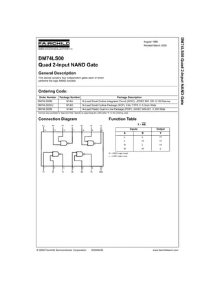


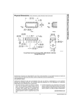

This document provides information on the DM74LS00 quad 2-input NAND gate integrated circuit from Fairchild Semiconductor. It contains four independent NAND gates that each perform the NAND logic function. The document lists the absolute maximum ratings, recommended operating conditions, electrical characteristics including switching characteristics, and physical dimensions for the 14-pin packages. It also contains a function table and connection diagram.


