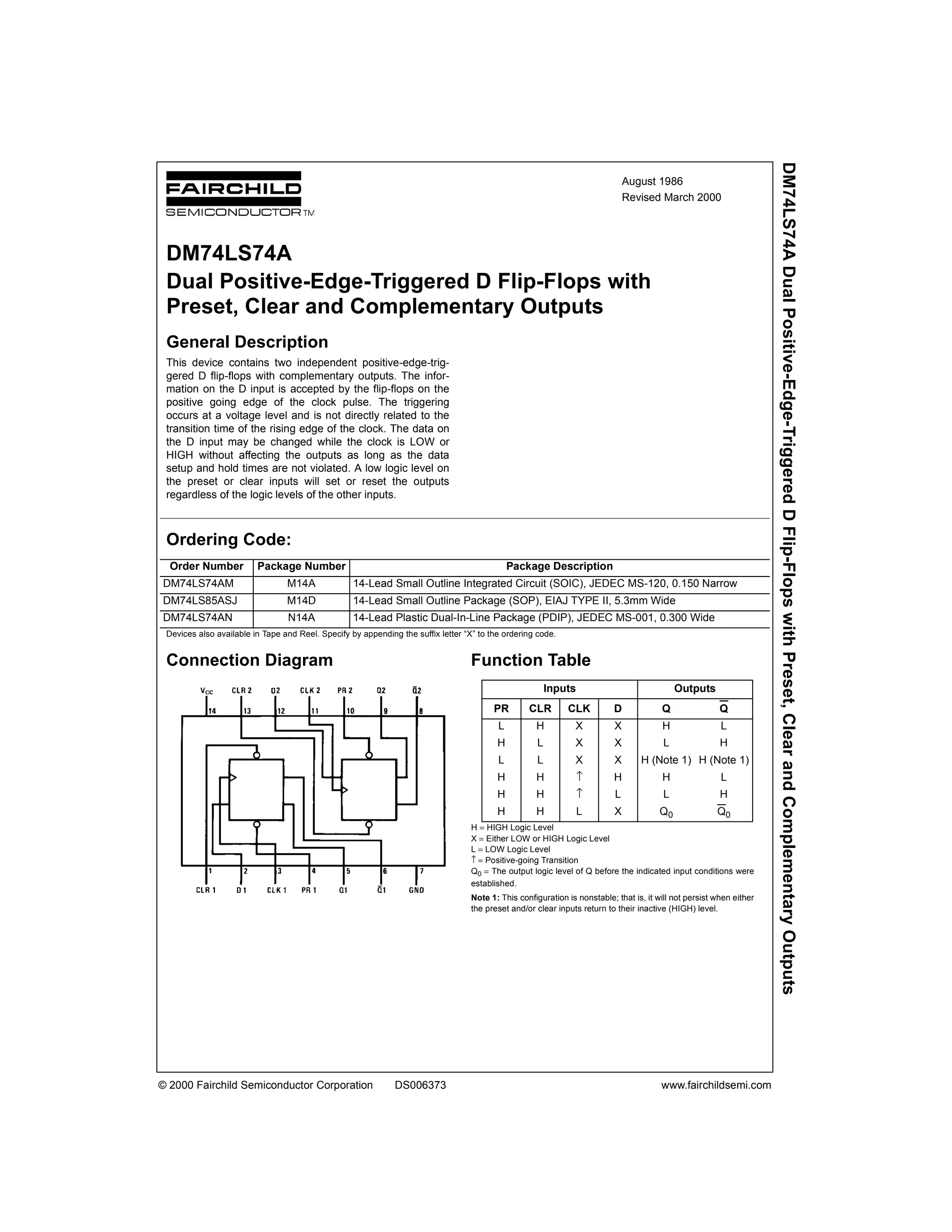
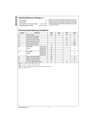
© 2000 Fairchild Semiconductor Corporation DS006373 www.fairchildsemi.com
August 1986
Revised March 2000
DM74LS74ADualPositive-Edge-TriggeredDFlip-FlopswithPreset,ClearandComplementaryOutputs
DM74LS74A
Dual Positive-Edge-Triggered D Flip-Flops with
Preset, Clear and Complementary Outputs
General Description
This device contains two independent positive-edge-trig-
gered D flip-flops with complementary outputs. The infor-
mation on the D input is accepted by the flip-flops on the
positive going edge of the clock pulse. The triggering
occurs at a voltage level and is not directly related to the
transition time of the rising edge of the clock. The data on
the D input may be changed while the clock is LOW or
HIGH without affecting the outputs as long as the data
setup and hold times are not violated. A low logic level on
the preset or clear inputs will set or reset the outputs
regardless of the logic levels of the other inputs.
Ordering Code:
Devices also available in Tape and Reel. Specify by appending the suffix letter “X” to the ordering code.
Connection Diagram Function Table
H = HIGH Logic Level
X = Either LOW or HIGH Logic Level
L = LOW Logic Level
↑ = Positive-going Transition
Q0 = The output logic level of Q before the indicated input conditions were
established.
Note 1: This configuration is nonstable; that is, it will not persist when either
the preset and/or clear inputs return to their inactive (HIGH) level.
Order Number Package Number Package Description
DM74LS74AM M14A 14-Lead Small Outline Integrated Circuit (SOIC), JEDEC MS-120, 0.150 Narrow
DM74LS85ASJ M14D 14-Lead Small Outline Package (SOP), EIAJ TYPE II, 5.3mm Wide
DM74LS74AN N14A 14-Lead Plastic Dual-In-Line Package (PDIP), JEDEC MS-001, 0.300 Wide
Inputs Outputs
PR CLR CLK D Q Q
L H X X H L
H L X X L H
L L X X H (Note 1) H (Note 1)
H H ↑ H H L
H H ↑ L L H
H H L X Q0 Q0
www.fairchildsemi.com 2
DM74LS74A
Absolute Maximum Ratings(Note 2)
Note 2: The “Absolute Maximum Ratings” are those values beyond which
the safety of the device cannot be guaranteed. The device should not be
operated at these limits. The parametric values defined in the Electrical
Characteristics tables are not guaranteed at the absolute maximum ratings.
The “Recommended Operating Conditions” table will define the conditions
for actual device operation.
Recommended Operating Conditions
Note 3: CL = 15 pF, RL = 2 kΩ, TA = 25°C, and VCC = 5V.
Note 4: CL = 50 pF, RL = 2 kΩ, TA = 25°C, and VCC = 5V.
Note 5: The symbol (↑) indicates the rising edge of the clock pulse is used for reference.
Note 6: TA = 25°C and VCC = 5V.
Supply Voltage 7V
Input Voltage 7V
Operating Free Air Temperature Range 0°C to +70°C
Storage Temperature Range −65°C to +150°C
Symbol Parameter Min Nom Max Units
VCC Supply Voltage 4.75 5 5.25 V
VIH HIGH Level Input Voltage 2 V
VIL LOW Level Input Voltage 0.8 V
IOH HIGH Level Output Current −0.4 mA
IOL LOW Level Output Current 8 mA
fCLK Clock Frequency (Note 3) 0 25 MHz
fCLK Clock Frequency (Note 4) 0 20 MHz
tW Pulse Width Clock HIGH 18
(Note 3) Preset LOW 15 ns
Clear LOW 15
tW Pulse Width Clock HIGH 25
(Note 4) Preset LOW 20 ns
Clear LOW 20
tSU Setup Time (Note 3)(Note 5) 20↑ ns
tSU Setup Time (Note 4)(Note 5) 25↑ ns
tH Hold Time (Note 5)(Note 6) 0↑ ns
TA Free Air Operating Temperature 0 70 °C
3 www.fairchildsemi.com
DM74LS74A
Electrical Characteristics
over recommended operating free air temperature range (unless otherwise noted)
Note 7: All typicals are at VCC = 5V, TA = 25°C.
Note 8: Not more than one output should be shorted at a time, and the duration should not exceed one second. For devices, with feedback from the outputs,
where shorting the outputs to ground may cause the outputs to change logic state an equivalent test may be performed where VO = 2.125V with the minimum
and maximum limits reduced by one half from their stated values. This is very useful when using automatic test equipment.
Note 9: With all outputs OPEN, ICC is measured with CLOCK grounded after setting the Q and Q outputs HIGH in turn.
Switching Characteristics
at VCC = 5V and TA = 25°C
Symbol Parameter Conditions Min
Typ
Max Units
(Note 7)
VI Input Clamp Voltage VCC = Min, II = −18 mA −1.5 V
VOH HIGH Level VCC = Min, IOH = Max
2.7 3.4 V
Output Voltage VIL = Max, VIH = Min
VOL LOW Level VCC = Min, IOL = Max
0.35 0.5
Output Voltage VIL = Max, VIH = Min V
IOL = 4 mA, VCC = Min 0.25 0.4
II Input Current @ Max VCC = Max Data 0.1
Input Voltage VI = 7V Clock 0.1
mA
Preset 0.2
Clear 0.2
IIH HIGH Level VCC = Max Data 20
Input Current VI = 2.7V Clock 20
µA
Clear 40
Preset 40
IIL LOW Level VCC = Max Data −0.4
Input Current VI = 0.4V Clock −0.4
mA
Preset −0.8
Clear −0.8
IOS Short Circuit Output Current VCC = Max (Note 8) −20 −100 mA
ICC Supply Current VCC = Max (Note 9) 4 8 mA
From (Input) RL = 2 kΩ
Symbol Parameter To (Output) CL = 15 pF CL = 50 pF Units
Min Max Min Max
fMAX Maximum Clock Frequency 25 20 MHz
tPLH Propagation Delay Time
Clock to Q or Q 25 35 ns
LOW-to-HIGH Level Output
tPHL Propagation Delay Time
Clock to Q or Q 30 35 ns
HIGH-to-LOW Level Output
tPLH Propagation Delay Time
Preset to Q 25 35 ns
LOW-to-HIGH Level Output
tPHL Propagation Delay Time
Preset to Q 30 35 ns
HIGH-to-LOW Level Output
tPLH Propagation Delay Time
Clear to Q 25 35 ns
LOW-to-HIGH Level Output
tPHL Propagation Delay Time
Clear to Q 30 35 ns
HIGH-to-LOW Level Output
www.fairchildsemi.com 4
DM74LS74A
Physical Dimensions inches (millimeters) unless otherwise noted
14-Lead Small Outline Integrated Circuit (SOIC), JEDEC MS-120, 0.150 Narrow
Package Number M14A
5 www.fairchildsemi.com
DM74LS74A
Physical Dimensions inches (millimeters) unless otherwise noted (Continued)
14-Lead Small Outline Package (SOP), EIAJ TYPE II, 5.3mm Wide
Package Number M14D
www.fairchildsemi.com 6
DM74LS74ADualPositive-Edge-TriggeredDFlip-FlopswithPreset,ClearandComplementaryOutputs
Physical Dimensions inches (millimeters) unless otherwise noted (Continued)
14-Lead Plastic Dual-In-Line Package (PDIP), JEDEC MS-001, 0.300 Wide
Package Number N14A
Fairchild does not assume any responsibility for use of any circuitry described, no circuit patent licenses are implied and
Fairchild reserves the right at any time without notice to change said circuitry and specifications.
LIFE SUPPORT POLICY
FAIRCHILD’S PRODUCTS ARE NOT AUTHORIZED FOR USE AS CRITICAL COMPONENTS IN LIFE SUPPORT
DEVICES OR SYSTEMS WITHOUT THE EXPRESS WRITTEN APPROVAL OF THE PRESIDENT OF FAIRCHILD
SEMICONDUCTOR CORPORATION. As used herein:
1. Life support devices or systems are devices or systems
which, (a) are intended for surgical implant into the
body, or (b) support or sustain life, and (c) whose failure
to perform when properly used in accordance with
instructions for use provided in the labeling, can be rea-
sonably expected to result in a significant injury to the
user.
2. A critical component in any component of a life support
device or system whose failure to perform can be rea-
sonably expected to cause the failure of the life support
device or system, or to affect its safety or effectiveness.
www.fairchildsemi.com

LS74

  • 1.
    © 2000 FairchildSemiconductor Corporation DS006373 www.fairchildsemi.com August 1986 Revised March 2000 DM74LS74ADualPositive-Edge-TriggeredDFlip-FlopswithPreset,ClearandComplementaryOutputs DM74LS74A Dual Positive-Edge-Triggered D Flip-Flops with Preset, Clear and Complementary Outputs General Description This device contains two independent positive-edge-trig- gered D flip-flops with complementary outputs. The infor- mation on the D input is accepted by the flip-flops on the positive going edge of the clock pulse. The triggering occurs at a voltage level and is not directly related to the transition time of the rising edge of the clock. The data on the D input may be changed while the clock is LOW or HIGH without affecting the outputs as long as the data setup and hold times are not violated. A low logic level on the preset or clear inputs will set or reset the outputs regardless of the logic levels of the other inputs. Ordering Code: Devices also available in Tape and Reel. Specify by appending the suffix letter “X” to the ordering code. Connection Diagram Function Table H = HIGH Logic Level X = Either LOW or HIGH Logic Level L = LOW Logic Level ↑ = Positive-going Transition Q0 = The output logic level of Q before the indicated input conditions were established. Note 1: This configuration is nonstable; that is, it will not persist when either the preset and/or clear inputs return to their inactive (HIGH) level. Order Number Package Number Package Description DM74LS74AM M14A 14-Lead Small Outline Integrated Circuit (SOIC), JEDEC MS-120, 0.150 Narrow DM74LS85ASJ M14D 14-Lead Small Outline Package (SOP), EIAJ TYPE II, 5.3mm Wide DM74LS74AN N14A 14-Lead Plastic Dual-In-Line Package (PDIP), JEDEC MS-001, 0.300 Wide Inputs Outputs PR CLR CLK D Q Q L H X X H L H L X X L H L L X X H (Note 1) H (Note 1) H H ↑ H H L H H ↑ L L H H H L X Q0 Q0
  • 2.
    www.fairchildsemi.com 2 DM74LS74A Absolute MaximumRatings(Note 2) Note 2: The “Absolute Maximum Ratings” are those values beyond which the safety of the device cannot be guaranteed. The device should not be operated at these limits. The parametric values defined in the Electrical Characteristics tables are not guaranteed at the absolute maximum ratings. The “Recommended Operating Conditions” table will define the conditions for actual device operation. Recommended Operating Conditions Note 3: CL = 15 pF, RL = 2 kΩ, TA = 25°C, and VCC = 5V. Note 4: CL = 50 pF, RL = 2 kΩ, TA = 25°C, and VCC = 5V. Note 5: The symbol (↑) indicates the rising edge of the clock pulse is used for reference. Note 6: TA = 25°C and VCC = 5V. Supply Voltage 7V Input Voltage 7V Operating Free Air Temperature Range 0°C to +70°C Storage Temperature Range −65°C to +150°C Symbol Parameter Min Nom Max Units VCC Supply Voltage 4.75 5 5.25 V VIH HIGH Level Input Voltage 2 V VIL LOW Level Input Voltage 0.8 V IOH HIGH Level Output Current −0.4 mA IOL LOW Level Output Current 8 mA fCLK Clock Frequency (Note 3) 0 25 MHz fCLK Clock Frequency (Note 4) 0 20 MHz tW Pulse Width Clock HIGH 18 (Note 3) Preset LOW 15 ns Clear LOW 15 tW Pulse Width Clock HIGH 25 (Note 4) Preset LOW 20 ns Clear LOW 20 tSU Setup Time (Note 3)(Note 5) 20↑ ns tSU Setup Time (Note 4)(Note 5) 25↑ ns tH Hold Time (Note 5)(Note 6) 0↑ ns TA Free Air Operating Temperature 0 70 °C
  • 3.
    3 www.fairchildsemi.com DM74LS74A Electrical Characteristics overrecommended operating free air temperature range (unless otherwise noted) Note 7: All typicals are at VCC = 5V, TA = 25°C. Note 8: Not more than one output should be shorted at a time, and the duration should not exceed one second. For devices, with feedback from the outputs, where shorting the outputs to ground may cause the outputs to change logic state an equivalent test may be performed where VO = 2.125V with the minimum and maximum limits reduced by one half from their stated values. This is very useful when using automatic test equipment. Note 9: With all outputs OPEN, ICC is measured with CLOCK grounded after setting the Q and Q outputs HIGH in turn. Switching Characteristics at VCC = 5V and TA = 25°C Symbol Parameter Conditions Min Typ Max Units (Note 7) VI Input Clamp Voltage VCC = Min, II = −18 mA −1.5 V VOH HIGH Level VCC = Min, IOH = Max 2.7 3.4 V Output Voltage VIL = Max, VIH = Min VOL LOW Level VCC = Min, IOL = Max 0.35 0.5 Output Voltage VIL = Max, VIH = Min V IOL = 4 mA, VCC = Min 0.25 0.4 II Input Current @ Max VCC = Max Data 0.1 Input Voltage VI = 7V Clock 0.1 mA Preset 0.2 Clear 0.2 IIH HIGH Level VCC = Max Data 20 Input Current VI = 2.7V Clock 20 µA Clear 40 Preset 40 IIL LOW Level VCC = Max Data −0.4 Input Current VI = 0.4V Clock −0.4 mA Preset −0.8 Clear −0.8 IOS Short Circuit Output Current VCC = Max (Note 8) −20 −100 mA ICC Supply Current VCC = Max (Note 9) 4 8 mA From (Input) RL = 2 kΩ Symbol Parameter To (Output) CL = 15 pF CL = 50 pF Units Min Max Min Max fMAX Maximum Clock Frequency 25 20 MHz tPLH Propagation Delay Time Clock to Q or Q 25 35 ns LOW-to-HIGH Level Output tPHL Propagation Delay Time Clock to Q or Q 30 35 ns HIGH-to-LOW Level Output tPLH Propagation Delay Time Preset to Q 25 35 ns LOW-to-HIGH Level Output tPHL Propagation Delay Time Preset to Q 30 35 ns HIGH-to-LOW Level Output tPLH Propagation Delay Time Clear to Q 25 35 ns LOW-to-HIGH Level Output tPHL Propagation Delay Time Clear to Q 30 35 ns HIGH-to-LOW Level Output
  • 4.
    www.fairchildsemi.com 4 DM74LS74A Physical Dimensionsinches (millimeters) unless otherwise noted 14-Lead Small Outline Integrated Circuit (SOIC), JEDEC MS-120, 0.150 Narrow Package Number M14A
  • 5.
    5 www.fairchildsemi.com DM74LS74A Physical Dimensionsinches (millimeters) unless otherwise noted (Continued) 14-Lead Small Outline Package (SOP), EIAJ TYPE II, 5.3mm Wide Package Number M14D
  • 6.
    www.fairchildsemi.com 6 DM74LS74ADualPositive-Edge-TriggeredDFlip-FlopswithPreset,ClearandComplementaryOutputs Physical Dimensionsinches (millimeters) unless otherwise noted (Continued) 14-Lead Plastic Dual-In-Line Package (PDIP), JEDEC MS-001, 0.300 Wide Package Number N14A Fairchild does not assume any responsibility for use of any circuitry described, no circuit patent licenses are implied and Fairchild reserves the right at any time without notice to change said circuitry and specifications. LIFE SUPPORT POLICY FAIRCHILD’S PRODUCTS ARE NOT AUTHORIZED FOR USE AS CRITICAL COMPONENTS IN LIFE SUPPORT DEVICES OR SYSTEMS WITHOUT THE EXPRESS WRITTEN APPROVAL OF THE PRESIDENT OF FAIRCHILD SEMICONDUCTOR CORPORATION. As used herein: 1. Life support devices or systems are devices or systems which, (a) are intended for surgical implant into the body, or (b) support or sustain life, and (c) whose failure to perform when properly used in accordance with instructions for use provided in the labeling, can be rea- sonably expected to result in a significant injury to the user. 2. A critical component in any component of a life support device or system whose failure to perform can be rea- sonably expected to cause the failure of the life support device or system, or to affect its safety or effectiveness. www.fairchildsemi.com