
Recommended
Recommended
More Related Content
What's hot
What's hot (20)
Similar to Original Mosfet N-Channel SSM3K15FV OP SMD Code SOT-723 New
Similar to Original Mosfet N-Channel SSM3K15FV OP SMD Code SOT-723 New (17)
More from AUTHELECTRONIC
More from AUTHELECTRONIC (20)
Recently uploaded
Recently uploaded (20)
Original Mosfet N-Channel SSM3K15FV OP SMD Code SOT-723 New
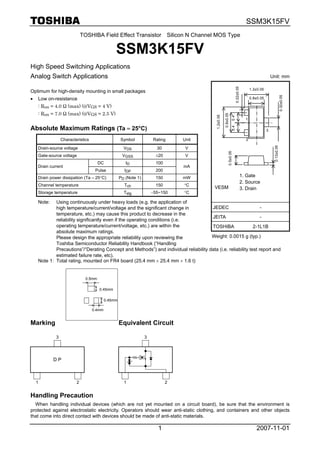
- 1. SSM3K15FV 2007-11-011 TOSHIBA Field Effect Transistor Silicon N Channel MOS Type SSM3K15FV High Speed Switching Applications Analog Switch Applications Optimum for high-density mounting in small packages • Low on-resistance : Ron = 4.0 Ω (max) (@VGS = 4 V) : Ron = 7.0 Ω (max) (@VGS = 2.5 V) Absolute Maximum Ratings (Ta = 25°C) Characteristics Symbol Rating Unit Drain-source voltage VDS 30 V Gate-source voltage VGSS ±20 V DC ID 100 Drain current Pulse IDP 200 mA Drain power dissipation (Ta = 25°C) PD (Note 1) 150 mW Channel temperature Tch 150 °C Storage temperature Tstg −55~150 °C Note: Using continuously under heavy loads (e.g. the application of high temperature/current/voltage and the significant change in temperature, etc.) may cause this product to decrease in the reliability significantly even if the operating conditions (i.e. operating temperature/current/voltage, etc.) are within the absolute maximum ratings. Please design the appropriate reliability upon reviewing the Toshiba Semiconductor Reliability Handbook (“Handling Precautions”/“Derating Concept and Methods”) and individual reliability data (i.e. reliability test report and estimated failure rate, etc). Note 1: Total rating, mounted on FR4 board (25.4 mm × 25.4 mm × 1.6 t) Marking Equivalent Circuit Handling Precaution When handling individual devices (which are not yet mounted on a circuit board), be sure that the environment is protected against electrostatic electricity. Operators should wear anti-static clothing, and containers and other objects that come into direct contact with devices should be made of anti-static materials. Unit: mm JEDEC - JEITA - TOSHIBA 2-1L1B Weight: 0.0015 g (typ.) 1. Gate 2. Source 3. DrainVESM 1.2±0.05 0.32±0.05 1 2 3 0.40.4 0.22±0.05 0.8±0.05 0.8±0.05 1.2±0.05 0.5±0.05 0.13±0.05 0.5mm 0.45mm 0.45mm 0.4mm D P 1 2 3 1 2 3
- 2. SSM3K15FV 2007-11-012 Electrical Characteristics (Ta = 25°C) Characteristics Symbol Test Condition Min Typ. Max Unit Gate leakage current IGSS VGS = ±16 V, VDS = 0 ⎯ ⎯ ±1 μA Drain-source breakdown voltage V (BR) DSS ID = 0.1 mA, VGS = 0 30 ⎯ ⎯ V Drain cut-off current IDSS VDS = 30 V, VGS = 0 ⎯ ⎯ 1 μA Gate threshold voltage Vth VDS = 3 V, ID = 0.1 mA 0.8 ⎯ 1.5 V Forward transfer admittance ⏐Yfs⏐ VDS = 3 V, ID = 10 mA 25 ⎯ ⎯ mS ID = 10 mA, VGS = 4 V ⎯ 2.2 4.0 Drain-Source on-resistance RDS (ON) ID = 10 mA, VGS = 2.5 V ⎯ 4.0 7.0 Ω Input capacitance Ciss VDS = 3 V, VGS = 0, f = 1 MHz ⎯ 7.8 ⎯ pF Reverse transfer capacitance Crss VDS = 3 V, VGS = 0, f = 1 MHz ⎯ 3.6 ⎯ pF Output capacitance Coss VDS = 3 V, VGS = 0, f = 1 MHz ⎯ 8.8 ⎯ pF Turn-on time ton ⎯ 50 ⎯ Switching time Turn-off time toff VDD = 5 V, ID = 10 mA, VGS = 0~5 V ⎯ 180 ⎯ ns Switching Time Test Circuit (a) Test circuit (b) VIN Precaution Vth can be expressed as the voltage between gate and source when the low operating current value is ID = 100 μA for this product. For normal switching operation, VGS (on) requires a higher voltage than Vth and VGS (off) requires a lower voltage than Vth. (The relationship can be established as follows: VGS (off) < Vth < VGS (on) ) Please take this into consideration when using the device. (c) VOUT ton 90% 10% 0 V 5 V 10% 90% toff tr tf VDD VDS (ON) VDD = 5 V D.U. <= 1% Input: tr, tf < 5 ns (Zout = 50 Ω) Common Source Ta = 25°C VDD Output Input 5 V 0 10 μs 50Ω RL
- 3. SSM3K15FV 2007-11-013 Drain-Sourceonresistance RDS(ON)(Ω) Drain-Sourceonresistance RDS(ON)(Ω) Drain-Source voltage VDS (V) ID – VDS DraincurrentID(mA) Gate-Source voltage VGS (V) ID – VGS DraincurrentID(mA) Drain current ID (mA) RDS (ON) – ID Drain-Sourceonresistance RDS(ON)(Ω) Gate-source voltage VGS (V) RDS (ON) – VGS Ambient temperature Ta (°C) RDS (ON) – Ta Ambient temperature Ta (°C) Vth – Ta GatethresholdvoltageVth(V) 0 −25 0.4 2 50 1501250 0.2 1.2 1.6 75 1 Common Source ID = 0.1 mA VDS = 3 V 0.8 1.8 25 100 0.6 1.4 0 0 100 250 1 21.50.5 50 150 200 VGS = 2.1 V 2.3 2.5 2.7 Common Source Ta = 25°C 3410 0 0 2 6 4 1082 1 4 5 6 3 25°C Ta = 100°C −25°C Common Source ID = 10 mA 0 −25 2 8 50 1501250 1 5 6 75 4 4 V VGS = 2.5 V Common Source ID = 10 mA 3 7 25 100 0.01 0 1 1000 2 431 0.1 10 100 Ta = 100°C Common Source VDS = 3 V −25°C25°C 4 V VGS = 2.5 V 0 0 4 10 80 20016040 2 6 8 120 Common Source Ta = 25°C
- 4. SSM3K15FV 2007-11-014 CapacitanceC(pF) Switchingtimet(ns) Drain current ID (mA) ⎪Yfs⎪ – ID Forwardtransferadmittance ⏐Yfs⏐(mS) Drain-Source voltage VDS (V) IDR – VDS DrainreverescurrentIDR(mA) Drain current ID (mA) t – ID Switchingtimet(ns) Drain current ID (mA) t – ID Drain-Source voltage VDS (V) C – VDS Ambient temperature Ta (°C) PD – Ta 1 1 10 30 1000 100 100010 100 3 5 50 300 500 Common Source VDS = 3 V Ta = 25°C 10 0.1 100 300 10000 1000 1001 10 30 50 500 3000 5000 Common Source VDD = 5 V VGS = 0~5 V Ta = 25°C tr ton tf toff 10 0.1 100 300 10000 1000 1001 10 30 50 500 3000 5000 Common Source VDD = 3 V VGS = 0~2.5 V Ta = 25°C tr ton tf toff 0.1 0.1 1 3 100 10 1001 10 0.3 0.5 5 30 50 Common Source VGS = 0 V f = 1 MHz Ta = 25°C Crss Coss Ciss 0 100 250 50 150 200 0 −1.4−0.4−0.2 −0.6 −0.8 −1 −1.2 Common Source VGS = 0 V Ta = 25°C G D S IDR DrainpowerdissipationPD(mW) 0 0 100 250 16040 50 150 200 20 60 80 100 140120 Mounted on FR4 board (25.4 mm × 25.4 mm × 1.6 t, Cu Pad: 0.585 mm 2 )
- 5. SSM3K15FV 2007-11-015 RESTRICTIONS ON PRODUCT USE 20070701-EN GENERAL • The information contained herein is subject to change without notice. • TOSHIBA is continually working to improve the quality and reliability of its products. Nevertheless, semiconductor devices in general can malfunction or fail due to their inherent electrical sensitivity and vulnerability to physical stress. It is the responsibility of the buyer, when utilizing TOSHIBA products, to comply with the standards of safety in making a safe design for the entire system, and to avoid situations in which a malfunction or failure of such TOSHIBA products could cause loss of human life, bodily injury or damage to property. In developing your designs, please ensure that TOSHIBA products are used within specified operating ranges as set forth in the most recent TOSHIBA products specifications. Also, please keep in mind the precautions and conditions set forth in the “Handling Guide for Semiconductor Devices,” or “TOSHIBA Semiconductor Reliability Handbook” etc. • The TOSHIBA products listed in this document are intended for usage in general electronics applications (computer, personal equipment, office equipment, measuring equipment, industrial robotics, domestic appliances, etc.).These TOSHIBA products are neither intended nor warranted for usage in equipment that requires extraordinarily high quality and/or reliability or a malfunction or failure of which may cause loss of human life or bodily injury (“Unintended Usage”). Unintended Usage include atomic energy control instruments, airplane or spaceship instruments, transportation instruments, traffic signal instruments, combustion control instruments, medical instruments, all types of safety devices, etc.. Unintended Usage of TOSHIBA products listed in his document shall be made at the customer’s own risk. • The products described in this document shall not be used or embedded to any downstream products of which manufacture, use and/or sale are prohibited under any applicable laws and regulations. • The information contained herein is presented only as a guide for the applications of our products. No responsibility is assumed by TOSHIBA for any infringements of patents or other rights of the third parties which may result from its use. No license is granted by implication or otherwise under any patents or other rights of TOSHIBA or the third parties. • Please contact your sales representative for product-by-product details in this document regarding RoHS compatibility. Please use these products in this document in compliance with all applicable laws and regulations that regulate the inclusion or use of controlled substances. Toshiba assumes no liability for damage or losses occurring as a result of noncompliance with applicable laws and regulations.