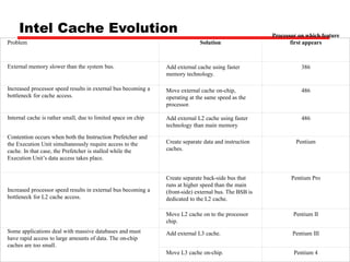
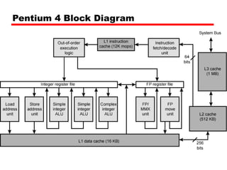
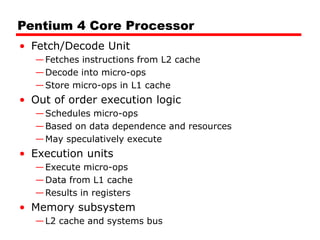
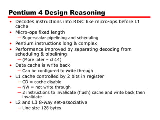
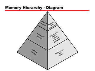
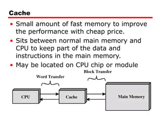
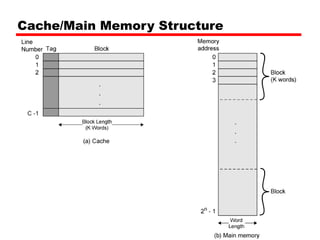
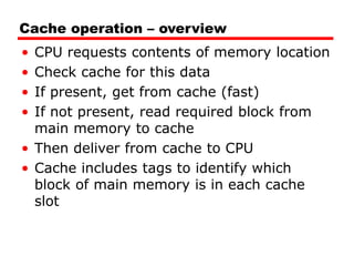
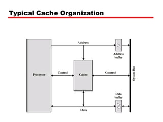
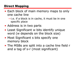
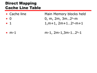
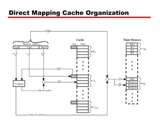
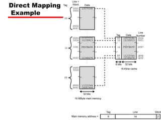
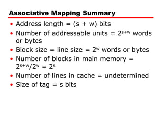
Cache memory is a small, fast memory located close to the CPU that stores frequently accessed instructions and data from main memory. It improves performance by reducing access time compared to main memory. There are three main characteristics of cache memory: 1) it uses the principle of locality of reference, where data that is accessed once is likely to be accessed again soon; 2) it is organized into blocks that are transferred between cache and main memory as a unit; and 3) it uses mapping and tagging to determine if requested data is in cache or needs to be fetched from main memory.
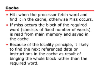
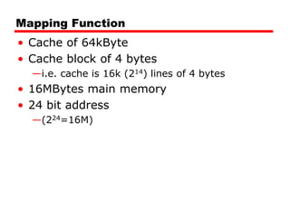
![Direct Mapping
Address Structure
Tag s-r Line or Slot r Word w
8 14 2
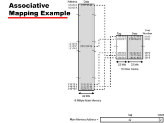
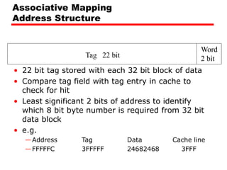
• 24 bit address
• 2 bit word identifier (4 byte block)
• 22 bit block identifier
— 8 bit tag (=22-14) [N.B. the no. of lines in the cache are 214=
16 K lines]
— 14 bit slot or line
• No two blocks in the same line have the same Tag field
• Check contents of cache by finding line and checking Tag](https://image.slidesharecdn.com/04cachememory-cust-240402031259-ed2be432/85/cache-memory-introduction-level-function-30-320.jpg)
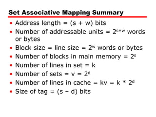
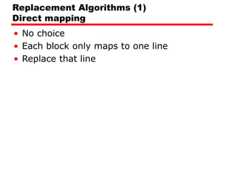
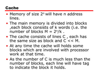
![Set Associative Mapping Summary
• If number of sets (v) = number of lines
(m) [i.e. number of lines for each set
k=1], the set associative technique will
convert to direct mapping.
• If k=m, v=1 (set associative will be fully
associative)
• The most common choice (v=m/2 and
k=2).
• Four way set associative means (k= 4 and
v=v/4).](https://image.slidesharecdn.com/04cachememory-cust-240402031259-ed2be432/85/cache-memory-introduction-level-function-47-320.jpg)