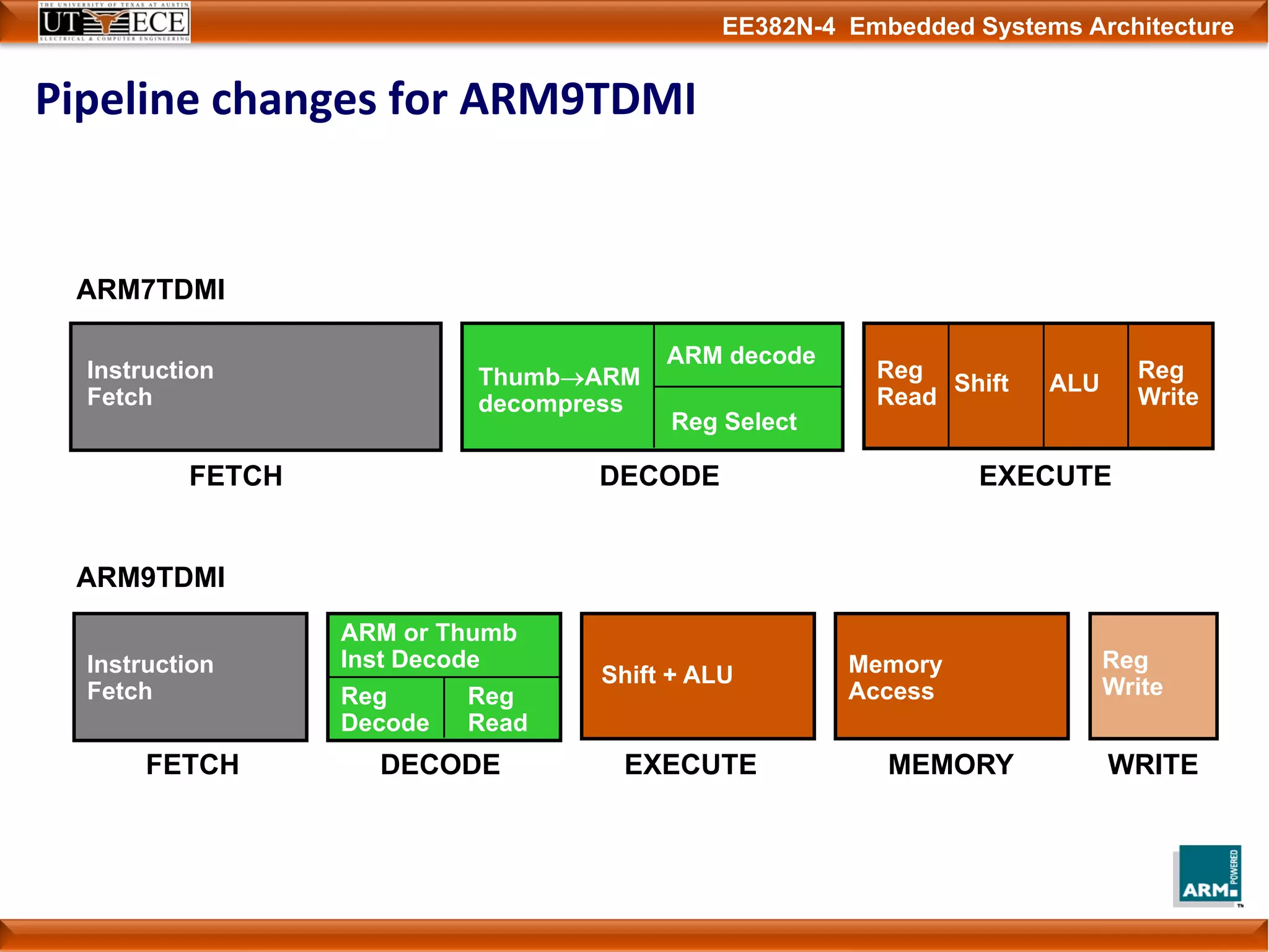
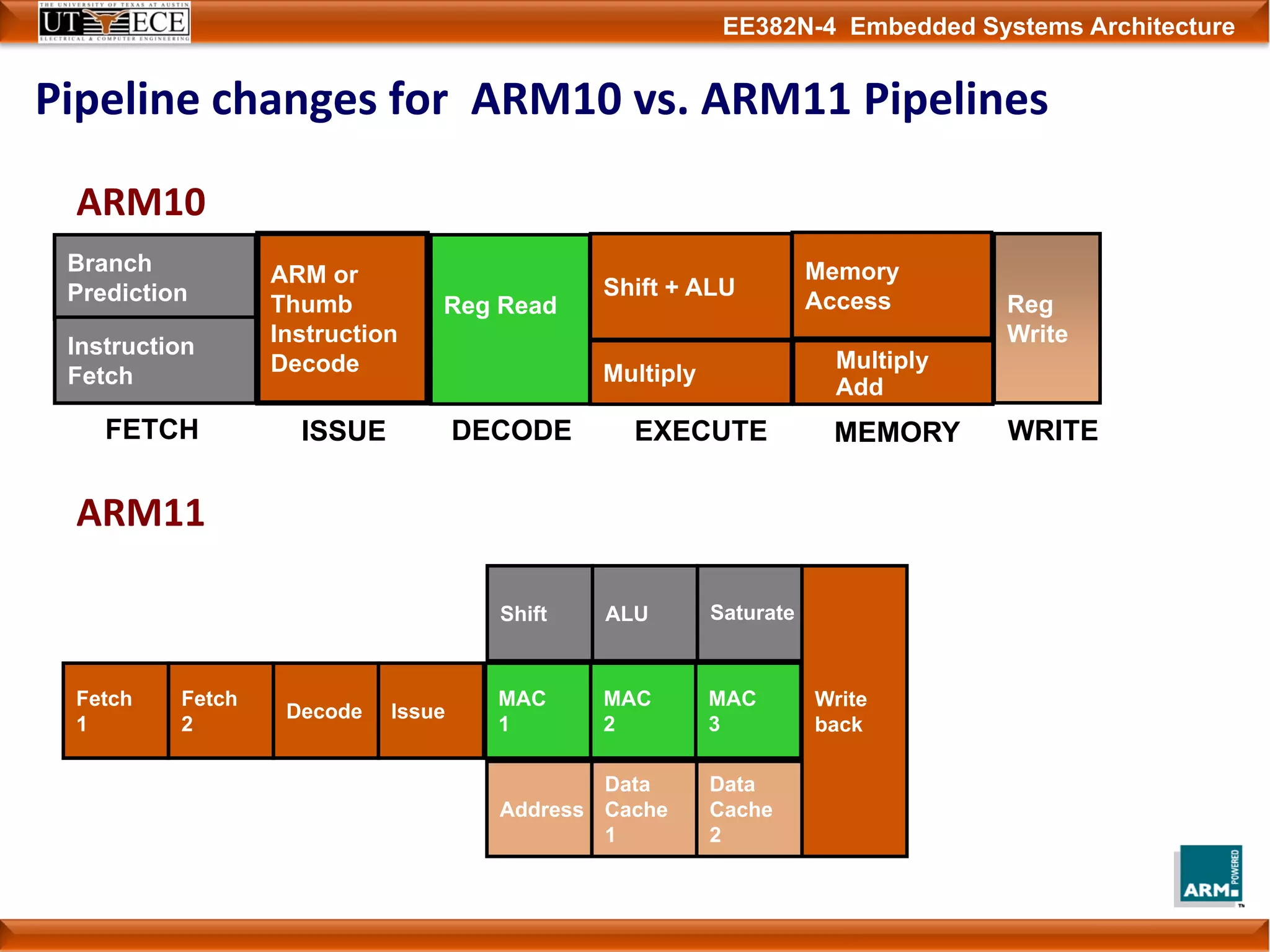
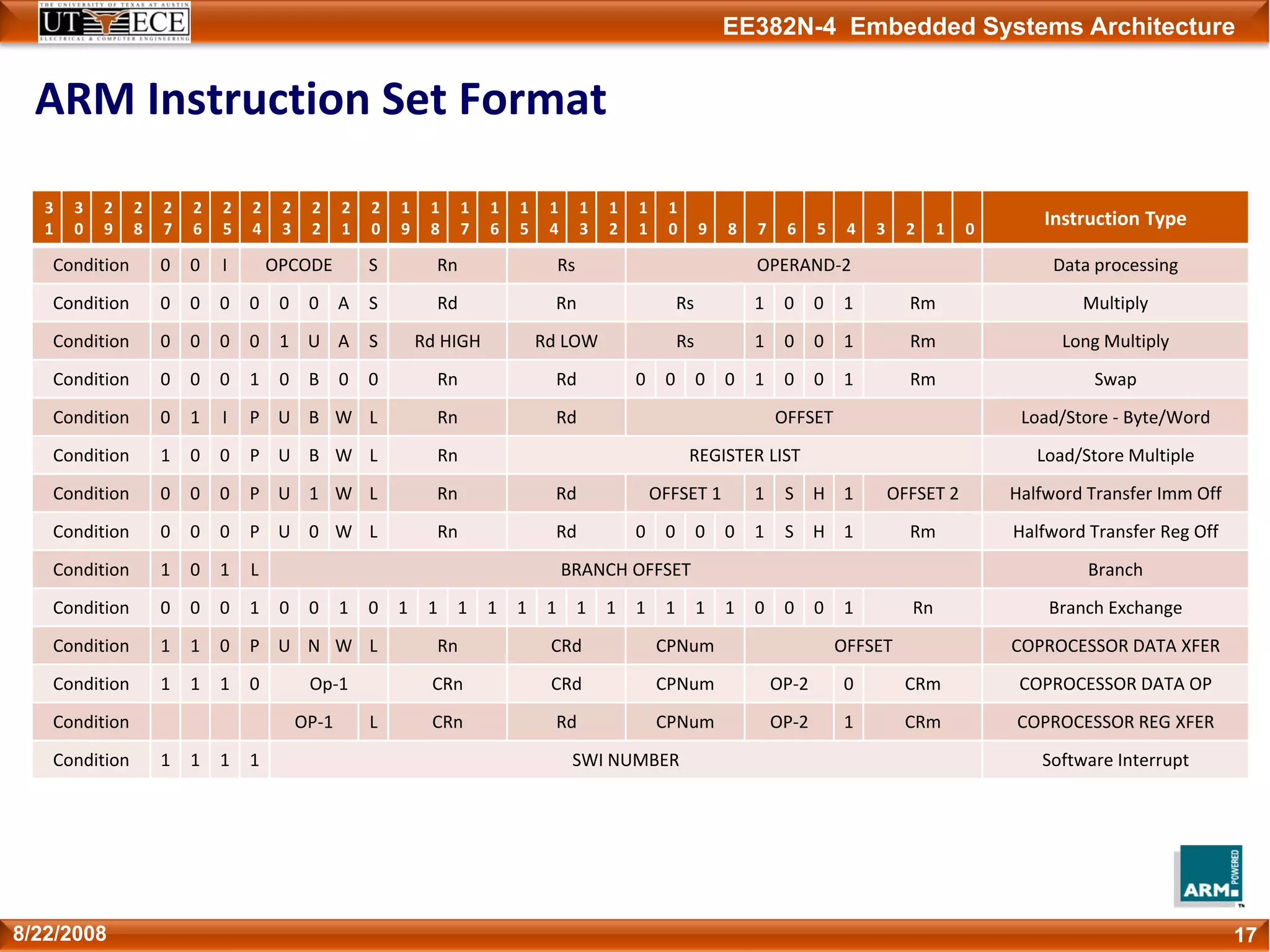
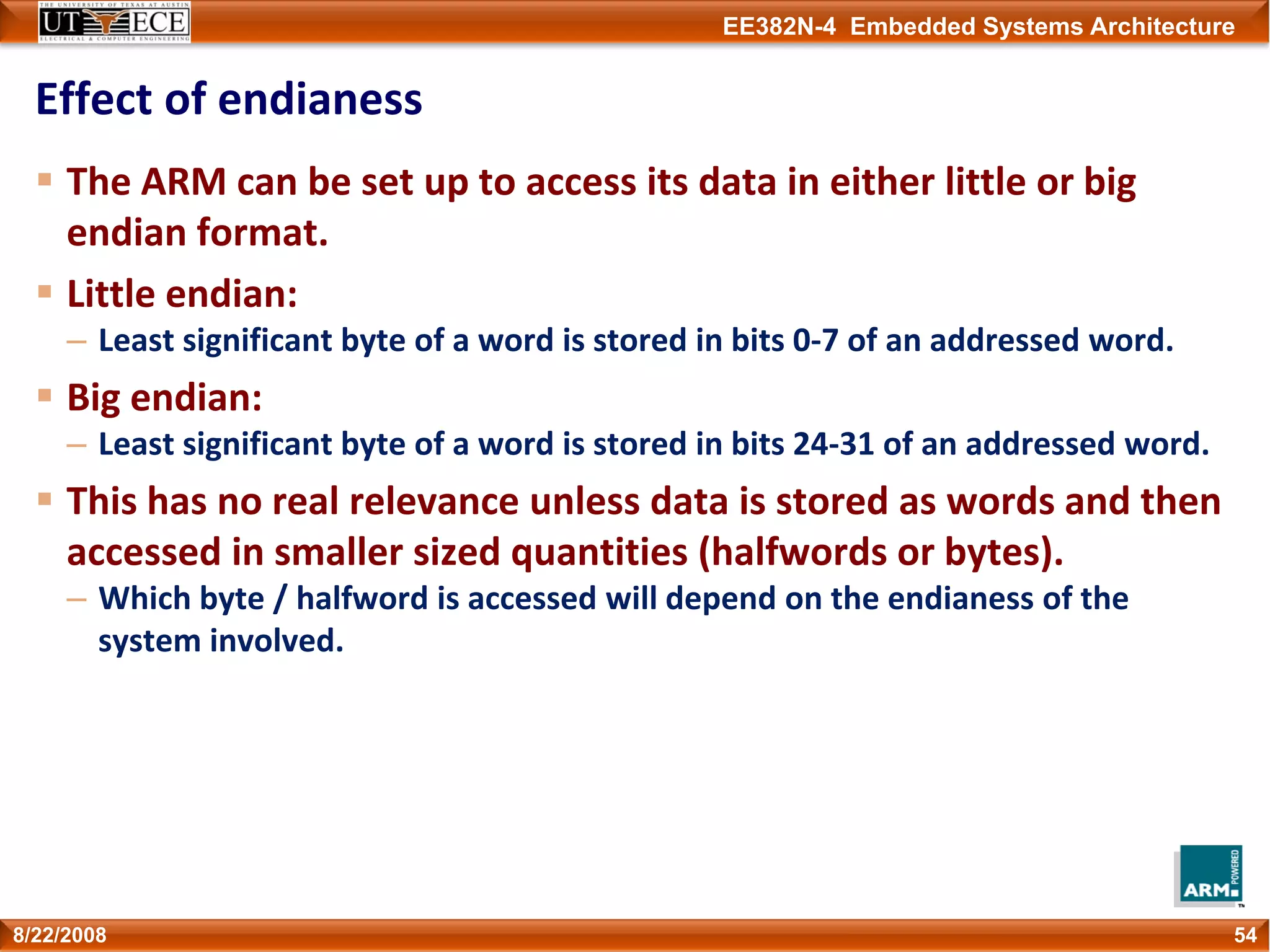
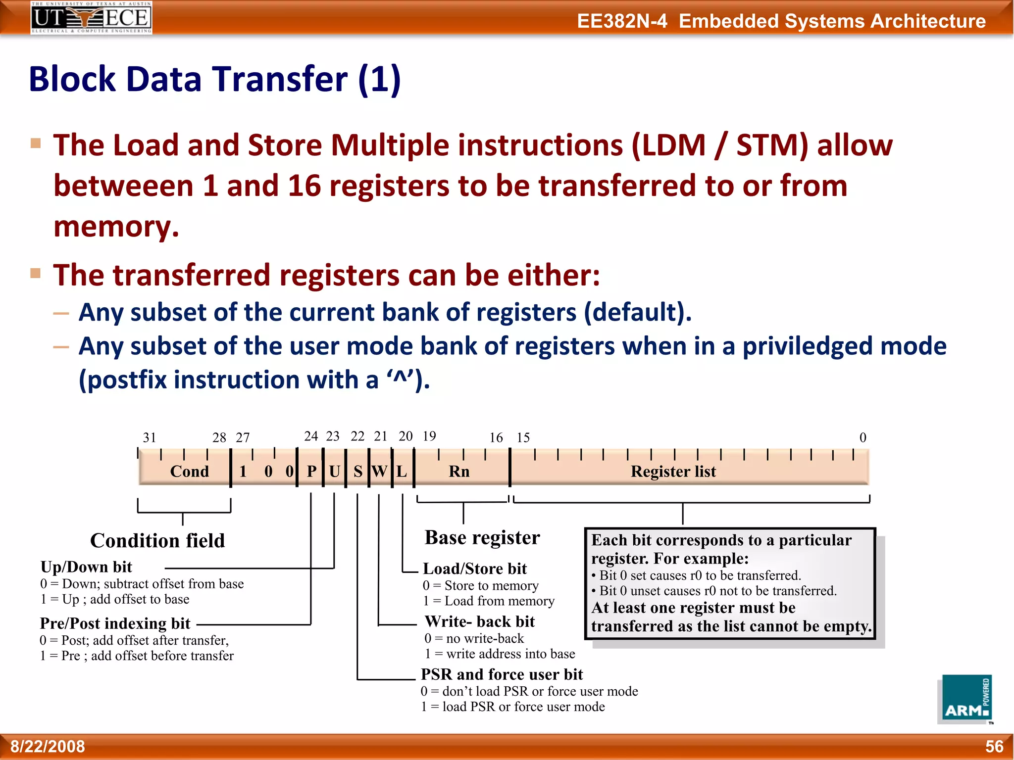
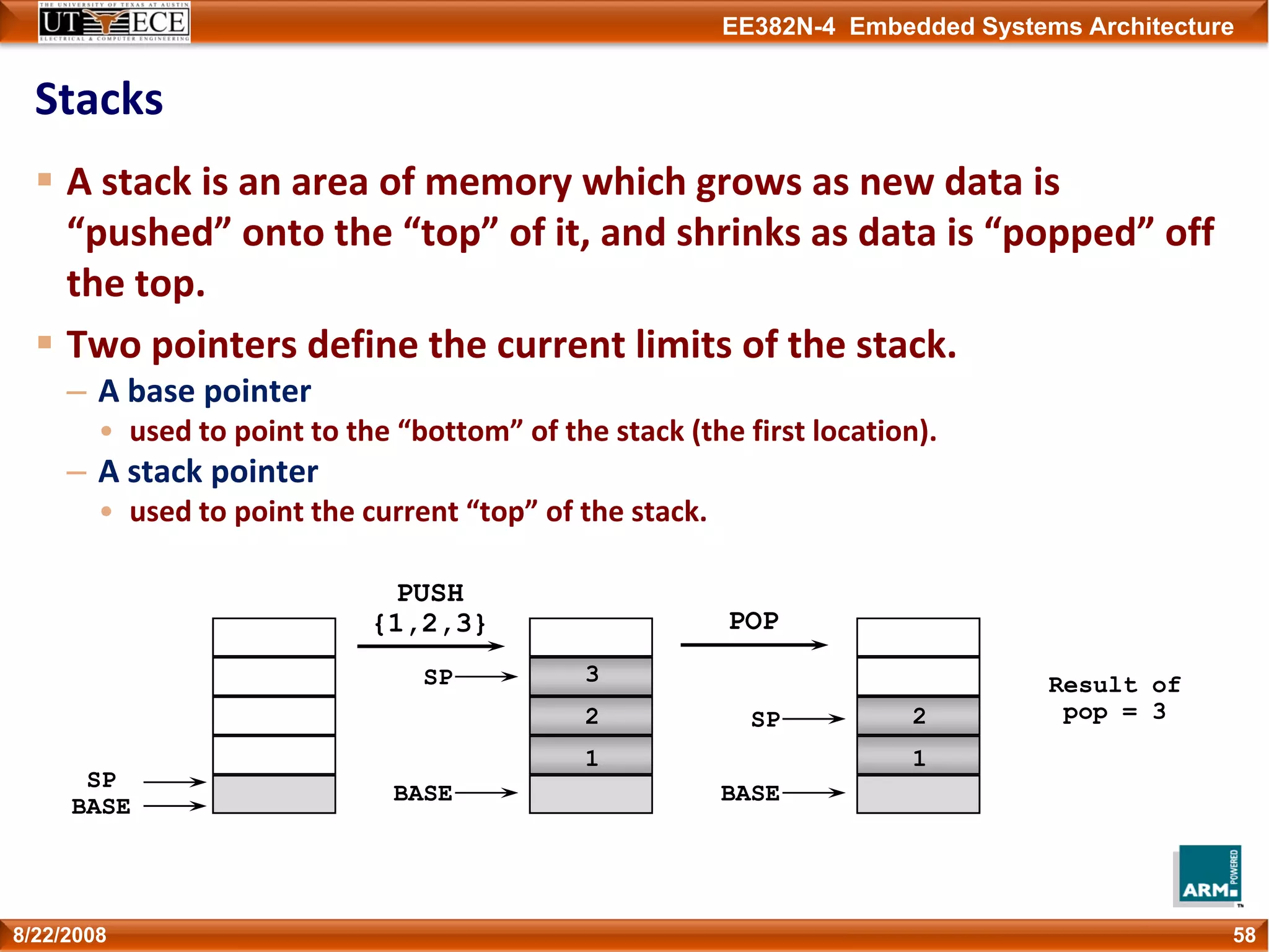
The document describes key aspects of the ARM instruction set architecture, including:
1) Instructions are 32-bits long and most execute in a single cycle. It uses a load/store architecture with separate memory access and data processing instructions.
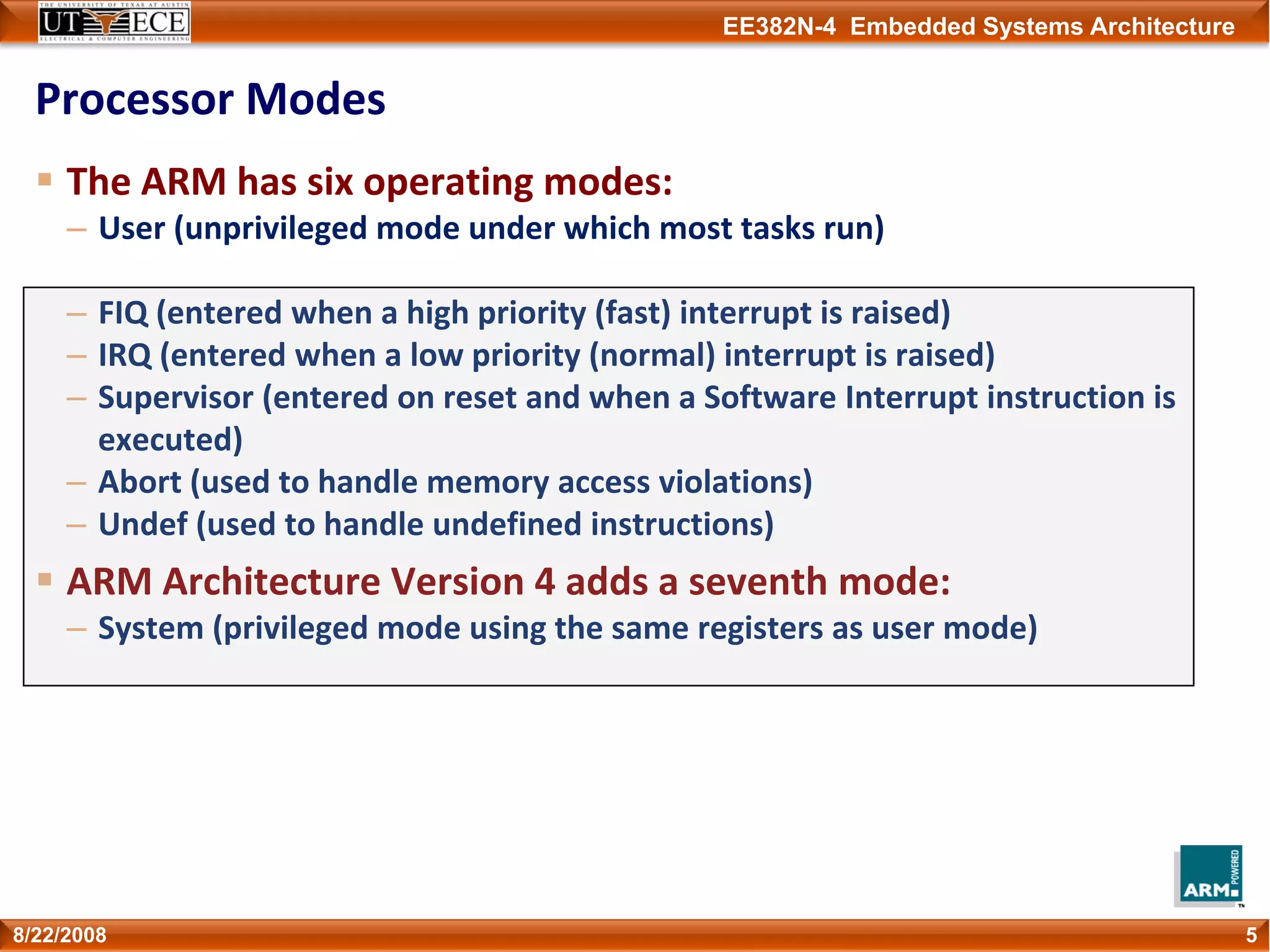
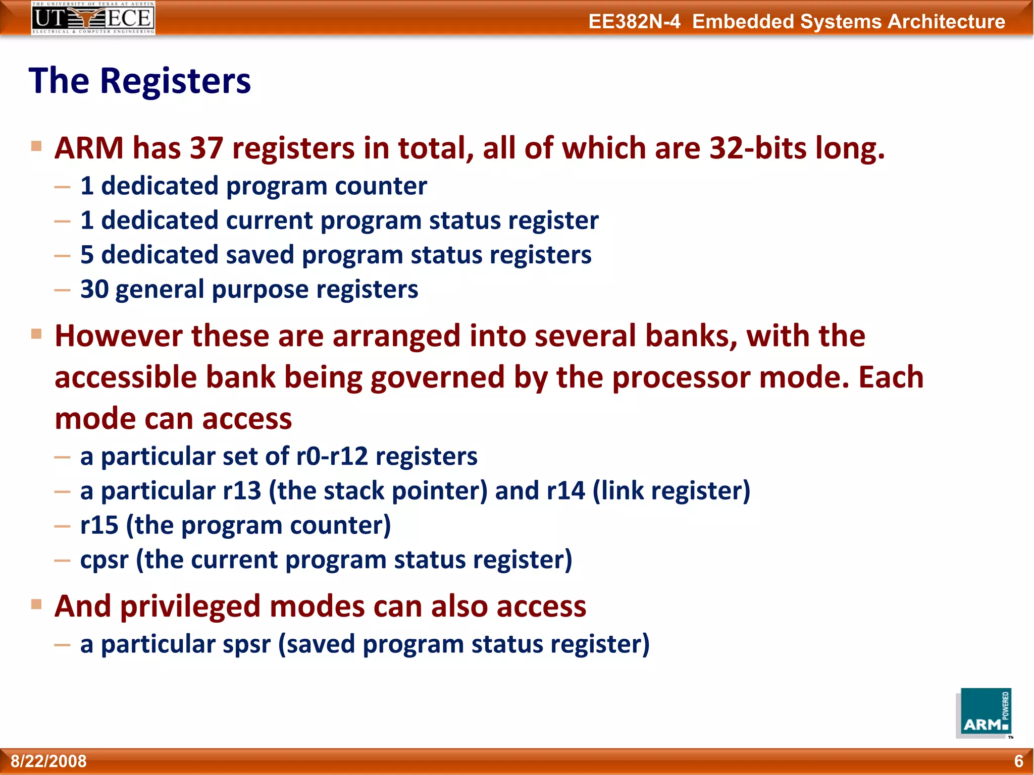
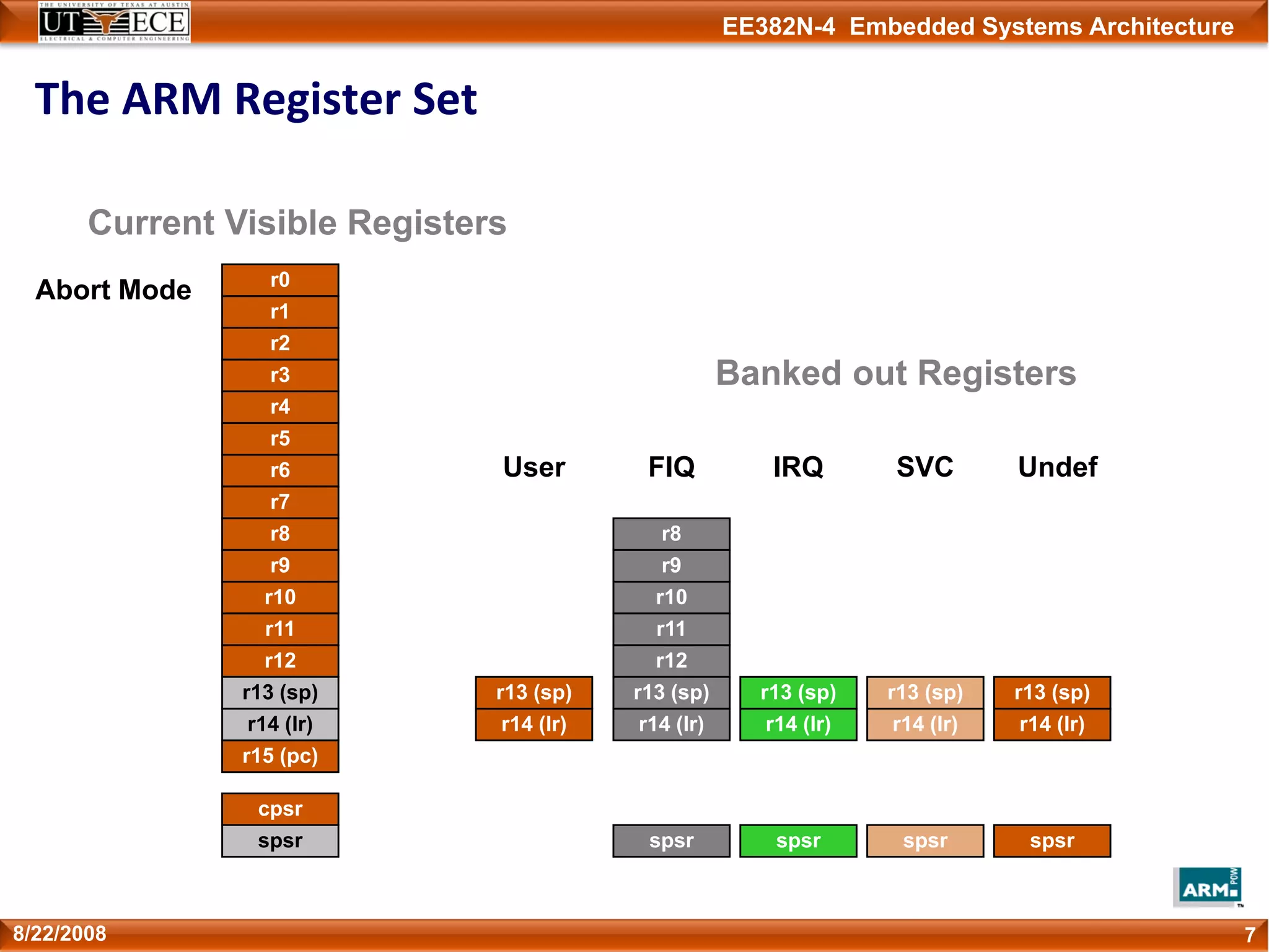
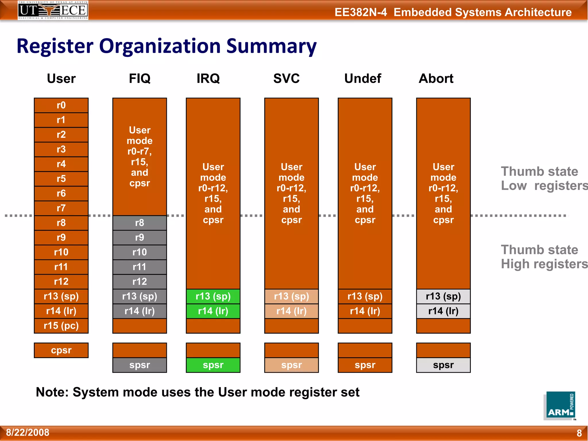
2) It has several processor modes for handling interrupts and exceptions. Registers are banked between modes to preserve their contents.
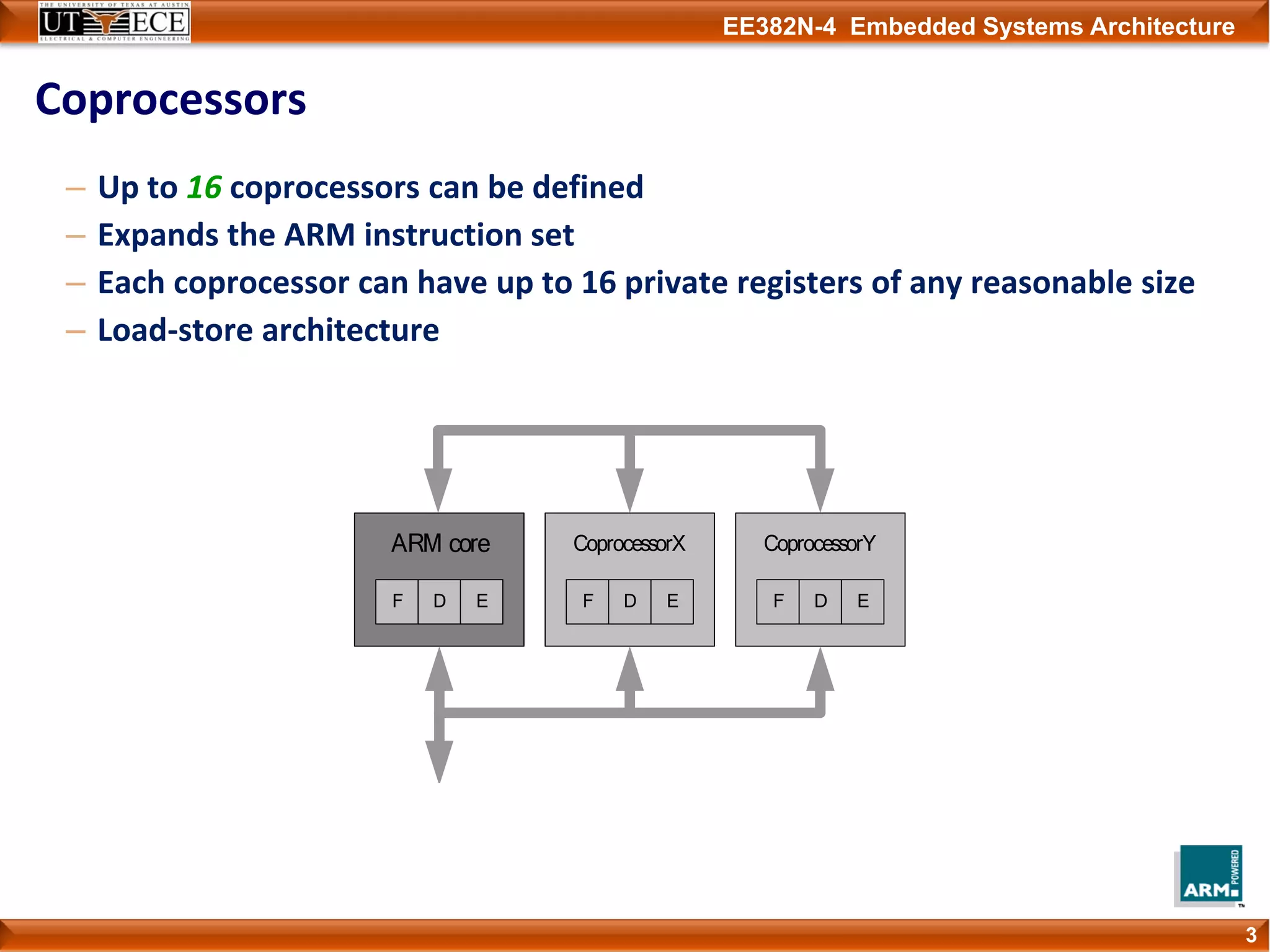
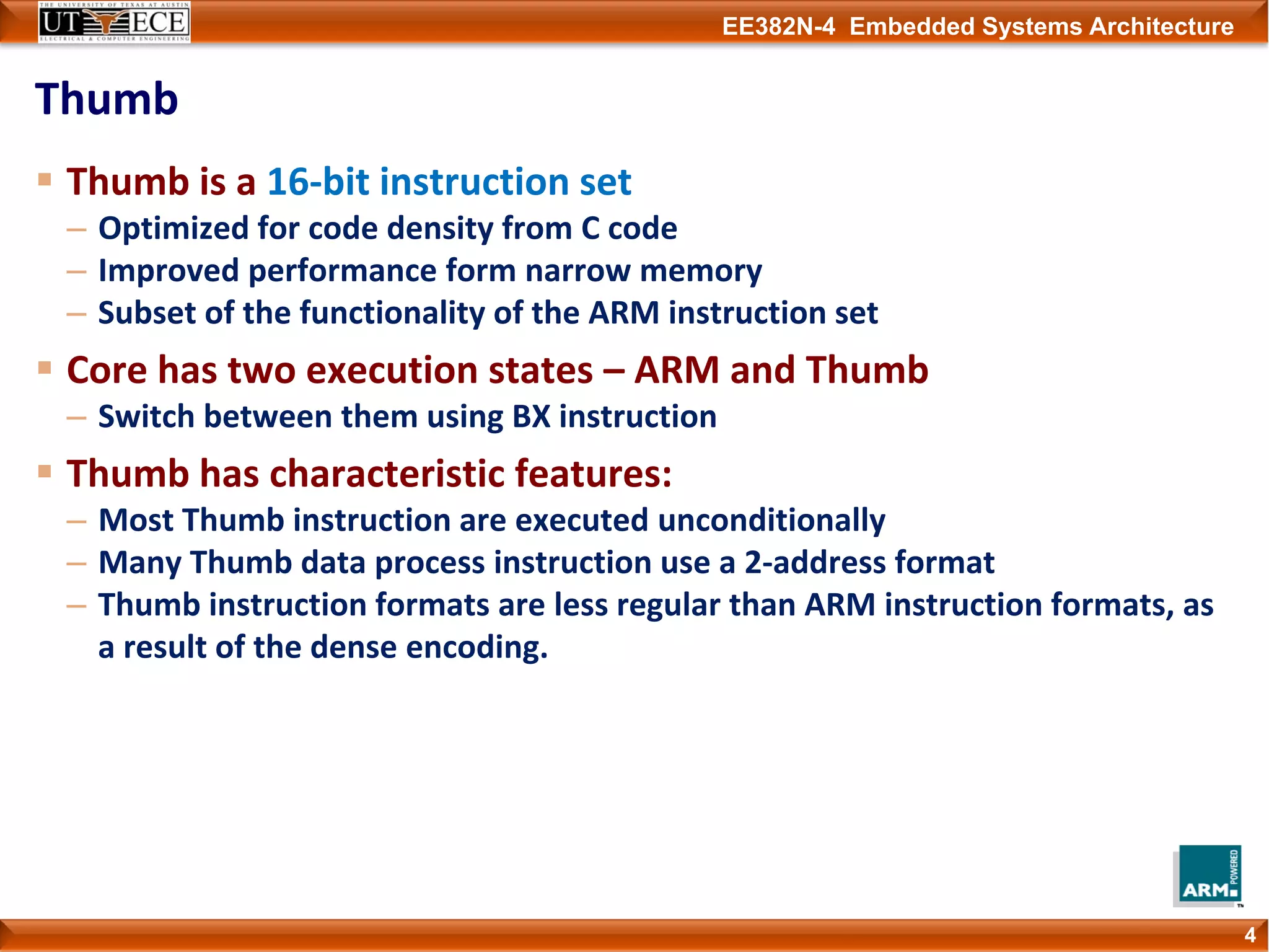
3) The instruction set can be extended through coprocessors and includes a compressed 16-bit Thumb instruction set for improved code density.
![EE382N-4 Embedded Systems Architecture
The Program Status Registers (CPSR and SPSRs)
108/22/2008
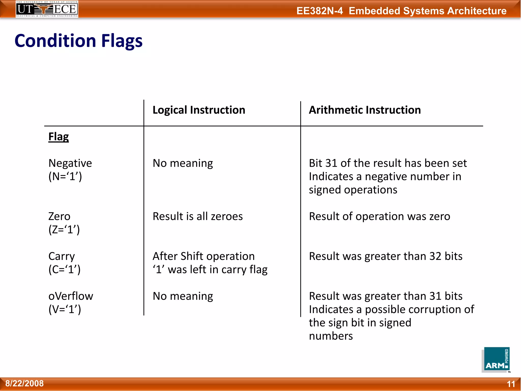
Copies of the ALU status flags (latched if the
instruction has the "S" bit set).
N = Negative result from ALU flag.
Z = Zero result from ALU flag.
C = ALU operation Carried out
V = ALU operation oVerflowed
* Interrupt Disable bits.
I = 1, disables the IRQ.
F = 1, disables the FIQ.
* T Bit (Architecture v4T only)
T = 0, Processor in ARM state
T = 1, Processor in Thumb state
* Condition Code Flags
ModeN Z C V
2831 8 4 0
I F T
* Mode Bits
M[4:0] define the processor mode.](https://image.slidesharecdn.com/armee382n4-150219005821-conversion-gate01/75/ARM-7-Detailed-instruction-set-10-2048.jpg)
![EE382N-4 Embedded Systems Architecture
The Program Counter (R15)
When the processor is executing in ARM state:
– All instructions are 32 bits in length
– All instructions must be word aligned
– Therefore the PC value is stored in bits [31:2] with bits [1:0] equal to zero (as
instruction cannot be halfword or byte aligned).
R14 is used as the subroutine link register (LR) and stores the
return address when Branch with Link operations are performed,
calculated from the PC.
Thus to return from a linked branch:
MOV r15,r14
or
MOV pc,lr
128/22/2008](https://image.slidesharecdn.com/armee382n4-150219005821-conversion-gate01/75/ARM-7-Detailed-instruction-set-12-2048.jpg)
![EE382N-4 Embedded Systems Architecture
Logical Operations
Operations are:
AND operand1 AND operand2
EOR operand1 EOR operand2
ORR operand1 OR operand2
ORN operand1 NOR operand2
BIC operand1 AND NOT operand2 [ie bit clear]
Syntax:
– <Operation>{<cond>}{S} Rd, Rn, Operand2
Examples:
AND r0, r1, r2
BICEQ r2, r3, #7
EORS r1,r3,r0
298/22/2008](https://image.slidesharecdn.com/armee382n4-150219005821-conversion-gate01/75/ARM-7-Detailed-instruction-set-29-2048.jpg)
![EE382N-4 Embedded Systems Architecture
Second Operand: Immediate Value (2)
This gives us:
– 0 ‐ 255 [0 ‐ 0xff]
– 256,260,264,..,1020 [0x100‐0x3fc, step 4, 0x40‐0xff ror 30]
– 1024,1040,1056,..,4080 [0x400‐0xff0, step 16, 0x40‐0xff ror 28]
– 4096,4160, 4224,..,16320 [0x1000‐0x3fc0, step 64, 0x40‐0xff ror 26]
These can be loaded using, for example:
– MOV r0, #0x40, 26 ; => MOV r0, #0x1000 (ie 4096)
To make this easier, the assembler will convert to this form for us if simply
given the required constant:
– MOV r0, #4096 ; => MOV r0, #0x1000 (ie 0x40 ror 26)
The bitwise complements can also be formed using MVN:
– MOV r0, #0xFFFFFFFF ; assembles to MVN r0, #0
If the required constant cannot be generated, an error will
be reported.
398/22/2008](https://image.slidesharecdn.com/armee382n4-150219005821-conversion-gate01/75/ARM-7-Detailed-instruction-set-39-2048.jpg)
![EE382N-4 Embedded Systems Architecture
Loading full 32 bit constants
Although the MOV/MVN mechanism will load a large range of constants into a
register, sometimes this mechanism will not generate the required constant.
Therefore, the assembler also provides a method which will load ANY 32 bit
constant:
– LDR rd,=numeric constant
If the constant can be constructed using either a MOV or MVN then this will be
the instruction actually generated.
Otherwise, the assembler will produce an LDR instruction with a PC‐relative
address to read the constant from a literal pool.
LDR r0,=0x42 ; generates MOV r0,#0x42
LDR r0,=0x55555555 ; generate LDR r0,[pc, offset to lit pool]
:
:
DCD 0x55555555
As this mechanism will always generate the best instruction for a given case, it
is the recommended way of loading constants.
408/22/2008](https://image.slidesharecdn.com/armee382n4-150219005821-conversion-gate01/75/ARM-7-Detailed-instruction-set-40-2048.jpg)
![EE382N-4 Embedded Systems Architecture
Load and Store Word or Byte: Base Register
The memory location to be accessed is held in a base register
STR r0, [r1] ; Store contents of r0 to location pointed to
; by contents of r1.
LDR r2, [r1] ; Load r2 with contents of memory location
; pointed to by contents of r1.
478/22/2008
r1
0x200
Base
Register
Memory
0x50x200
r0
0x5
Source
Register
for STR
r2
0x5
Destination
Register
for LDR](https://image.slidesharecdn.com/armee382n4-150219005821-conversion-gate01/75/ARM-7-Detailed-instruction-set-47-2048.jpg)
![EE382N-4 Embedded Systems Architecture
Load/Store Word or Byte: Pre‐indexed Addressing
Example: STR r0, [r1,#12]
– To store to location 0x1f4 instead use: STR r0, [r1,#‐12]
– To auto‐increment base pointer to 0x20c use: STR r0, [r1, #12]!
– If r2 contains 3, access 0x20c by multiplying this by 4:
• STR r0, [r1, r2, LSL #2]
498/22/2008
r1
0x200
Base
Register
Memory
0x5
0x200
r0
0x5
Source
Register
for STR
Offset
12 0x20c](https://image.slidesharecdn.com/armee382n4-150219005821-conversion-gate01/75/ARM-7-Detailed-instruction-set-49-2048.jpg)
![EE382N-4 Embedded Systems Architecture
Load and Store Word or Byte: Post‐indexed Addressing
Example: STR r0, [r1], #12
– To auto‐increment the base register to location 0x1f4 instead use:
• STR r0, [r1], #‐12
– If r2 contains 3, auto‐increment base register to 0x20c by multiplying this by
4:
• STR r0, [r1], r2, LSL #2
508/22/2008
r1
0x200
Original
Base
Register
Memory
0x50x200
r0
0x5
Source
Register
for STR
Offset
12 0x20c
r1
0x20c
Updated
Base
Register](https://image.slidesharecdn.com/armee382n4-150219005821-conversion-gate01/75/ARM-7-Detailed-instruction-set-50-2048.jpg)
![EE382N-4 Embedded Systems Architecture
Example Usage of Addressing Modes
Imagine an array, the first element of which is pointed to by the contents of r0.
If we want to access a particular element,
then we can use pre‐indexed addressing:
– r1 is element we want.
– LDR r2, [r0, r1, LSL #2]
If we want to step through every
element of the array, for instance
to produce sum of elements in the
array, then we can use post‐indexed addressing within a loop:
– r1 is address of current element (initially equal to r0).
– LDR r2, [r1], #4
Use a further register to store the address of final element,
so that the loop can be correctly terminated.
528/22/2008
0
1
2
3
element
0
4
8
12
Memory
Offset
r0
Pointer to
start of array](https://image.slidesharecdn.com/armee382n4-150219005821-conversion-gate01/75/ARM-7-Detailed-instruction-set-52-2048.jpg)
![EE382N-4 Embedded Systems Architecture
YA Endianess Example
558/22/2008
Big-endianLittle-endian
r1 = 0x100
r0 = 0x11223344
31 24 23 16 15 8 7 0
11 22 33 44
31 24 23 16 15 8 7 0
11 22 33 44
31 24 23 16 15 8 7 0
44 33 22 11
31 24 23 16 15 8 7 0
00 00 00 44
31 24 23 16 15 8 7 0
00 00 00 11
r2 = 0x44 r2 = 0x11
STR r0, [r1]
LDRB r2, [r1]
r1 = 0x100Memory](https://image.slidesharecdn.com/armee382n4-150219005821-conversion-gate01/75/ARM-7-Detailed-instruction-set-55-2048.jpg)
![EE382N-4 Embedded Systems Architecture
Swap and Swap Byte Instructions
Atomic operation of a memory read followed by a memory write
which moves byte or word quantities between registers and
memory.
Syntax:
– SWP{<cond>}{B} Rd, Rm, [Rn]
To implement an actual swap of contents make Rd = Rm.
The compiler cannot produce this instruction.
648/22/2008
Rm Rd
Rn
32
1
temp
Memory](https://image.slidesharecdn.com/armee382n4-150219005821-conversion-gate01/75/ARM-7-Detailed-instruction-set-64-2048.jpg)
![EE382N-4 Embedded Systems Architecture
Example: C assignments
C:
x = (a + b) - c;
Assembler:
ADR r4,a ; get address for a
LDR r0,[r4] ; get value of a
ADR r4,b ; get address for b, reusing r4
LDR r1,[r4] ; get value of b
ADD r3,r0,r1 ; compute a+b
ADR r4,c ; get address for c
LDR r2,[r4] ; get value of c
SUB r3,r3,r2 ; complete computation of x
ADR r4,x ; get address for x
STR r3,[r4] ; store value of x
718/22/2008
© 2008 Wayne Wolf Computers as Components 2nd ed.](https://image.slidesharecdn.com/armee382n4-150219005821-conversion-gate01/75/ARM-7-Detailed-instruction-set-71-2048.jpg)
![EE382N-4 Embedded Systems Architecture
Example: C assignment
C:
y = a*(b+c);
Assembler:
ADR r4,b ; get address for b
LDR r0,[r4] ; get value of b
ADR r4,c ; get address for c
LDR r1,[r4] ; get value of c
ADD r2,r0,r1 ; compute partial result
ADR r4,a ; get address for a
LDR r0,[r4] ; get value of a
MUL r2,r2,r0 ; compute final value for y
ADR r4,y ; get address for y
STR r2,[r4] ; store y
728/22/2008
© 2008 Wayne Wolf Computers as Components 2nd ed.](https://image.slidesharecdn.com/armee382n4-150219005821-conversion-gate01/75/ARM-7-Detailed-instruction-set-72-2048.jpg)
![EE382N-4 Embedded Systems Architecture
Example: C assignment
C:
z = (a << 2) | (b & 15);
Assembler:
ADR r4,a ; get address for a
LDR r0,[r4] ; get value of a
MOV r0,r0,LSL 2 ; perform shift
ADR r4,b ; get address for b
LDR r1,[r4] ; get value of b
AND r1,r1,#15 ; perform AND
ORR r1,r0,r1 ; perform OR
ADR r4,z ; get address for z
STR r1,[r4] ; store value for z
738/22/2008
© 2008 Wayne Wolf Computers as Components 2nd ed.](https://image.slidesharecdn.com/armee382n4-150219005821-conversion-gate01/75/ARM-7-Detailed-instruction-set-73-2048.jpg)
![EE382N-4 Embedded Systems Architecture
Example: if statement
C:
if (a > b) { x = 5; y = c + d; } else x = c - d;
Assembler:
; compute and test condition
ADR r4,a ; get address for a
LDR r0,[r4] ; get value of a
ADR r4,b ; get address for b
LDR r1,[r4] ; get value for b
CMP r0,r1 ; compare a < b
BLE fblock ; if a ><= b, branch to false block
748/22/2008
© 2008 Wayne Wolf Computers as Components 2nd ed.](https://image.slidesharecdn.com/armee382n4-150219005821-conversion-gate01/75/ARM-7-Detailed-instruction-set-74-2048.jpg)
![EE382N-4 Embedded Systems Architecture
if statement, cont’d.
; true block
MOV r0,#5 ; generate value for x
ADR r4,x ; get address for x
STR r0,[r4] ; store x
ADR r4,c ; get address for c
LDR r0,[r4] ; get value of c
ADR r4,d ; get address for d
LDR r1,[r4] ; get value of d
ADD r0,r0,r1 ; compute y
ADR r4,y ; get address for y
STR r0,[r4] ; store y
B after ; branch around false block
758/22/2008
© 2008 Wayne Wolf Computers as Components 2nd ed.](https://image.slidesharecdn.com/armee382n4-150219005821-conversion-gate01/75/ARM-7-Detailed-instruction-set-75-2048.jpg)
![EE382N-4 Embedded Systems Architecture
if statement, cont’d.
; false block
fblock ADR r4,c ; get address for c
LDR r0,[r4] ; get value of c
ADR r4,d ; get address for d
LDR r1,[r4] ; get value for d
SUB r0,r0,r1 ; compute a-b
ADR r4,x ; get address for x
STR r0,[r4] ; store value of x
after ...
768/22/2008
© 2008 Wayne Wolf Computers as Components 2nd ed.](https://image.slidesharecdn.com/armee382n4-150219005821-conversion-gate01/75/ARM-7-Detailed-instruction-set-76-2048.jpg)
![EE382N-4 Embedded Systems Architecture
Example: Conditional instruction implementation
; true block
MOVLT r0,#5 ; generate value for x
ADRLT r4,x ; get address for x
STRLT r0,[r4] ; store x
ADRLT r4,c ; get address for c
LDRLT r0,[r4] ; get value of c
ADRLT r4,d ; get address for d
LDRLT r1,[r4] ; get value of d
ADDLT r0,r0,r1 ; compute y
ADRLT r4,y ; get address for y
STRLT r0,[r4] ; store y
778/22/2008
© 2008 Wayne Wolf Computers as Components 2nd ed.](https://image.slidesharecdn.com/armee382n4-150219005821-conversion-gate01/75/ARM-7-Detailed-instruction-set-77-2048.jpg)
![EE382N-4 Embedded Systems Architecture
Conditional instruction implementation, cont’d.
; false block
ADRGE r4,c ; get address for c
LDRGE r0,[r4] ; get value of c
ADRGE r4,d ; get address for d
LDRGE r1,[r4] ; get value for d
SUBGE r0,r0,r1 ; compute a-b
ADRGE r4,x ; get address for x
STRGE r0,[r4] ; store value of x
788/22/2008
© 2008 Wayne Wolf Computers as Components 2nd ed.](https://image.slidesharecdn.com/armee382n4-150219005821-conversion-gate01/75/ARM-7-Detailed-instruction-set-78-2048.jpg)
![EE382N-4 Embedded Systems Architecture
Example: switch statement
C:
switch (test) { case 0: … break; case 1: … }
Assembler:
ADR r2,test ; get address for test
LDR r0,[r2] ; load value for test
ADR r1,switchtab ; load address for switch table
LDR r1,[r1,r0,LSL #2] ; index switch table
switchtab DCD case0
DCD case1
...
798/22/2008
© 2008 Wayne Wolf Computers as Components 2nd ed.](https://image.slidesharecdn.com/armee382n4-150219005821-conversion-gate01/75/ARM-7-Detailed-instruction-set-79-2048.jpg)
![EE382N-4 Embedded Systems Architecture
Example: FIR filter
C:
for (i=0, f=0; i<N; i++)
f = f + c[i]*x[i];
Assembler
; loop initiation code
MOV r0,#0 ; use r0 for I
MOV r8,#0 ; use separate index for arrays
ADR r2,N ; get address for N
LDR r1,[r2] ; get value of N
MOV r2,#0 ; use r2 for f
808/22/2008
© 2008 Wayne Wolf Computers as Components 2nd ed.](https://image.slidesharecdn.com/armee382n4-150219005821-conversion-gate01/75/ARM-7-Detailed-instruction-set-80-2048.jpg)
![EE382N-4 Embedded Systems Architecture
FIR filter, cont’.d
ADR r3,c ; load r3 with base of c
ADR r5,x ; load r5 with base of x
; loop body
loop LDR r4,[r3,r8] ; get c[i]
LDR r6,[r5,r8] ; get x[i]
MUL r4,r4,r6 ; compute c[i]*x[i]
ADD r2,r2,r4 ; add into running sum
ADD r8,r8,#4 ; add one word offset to array index
ADD r0,r0,#1 ; add 1 to i
CMP r0,r1 ; exit?
BLT loop ; if i < N, continue
818/22/2008
© 2008 Wayne Wolf Computers as Components 2nd ed.](https://image.slidesharecdn.com/armee382n4-150219005821-conversion-gate01/75/ARM-7-Detailed-instruction-set-81-2048.jpg)