Download to read offline

![103 International Journal for Modern Trends in Science and Technology
Kanike Anjali and R. Varaprasad Rao : An Energy Efficiency Systematic Cell Design Methodology Using Inputs XOR
& XNOR
II. RELATED WORK
Subsisting work
In this section, we will visually perceive the
three-input XOR/XNOR circuits to examine their
high performance. In complementary CMOS logic
the pull-down and pull-up networks utilized in the
circuit perform the function in a complementary
way. It has high noise margin and no static power
consumption. In the CMOS with transmission gate,
there is a advantage of utilizing less number of
transistors. In complementary pass-transistor, it
has a good output driving capability and
pass-transistor logics gain their celerity over the
CMOS due to their high logic functionality. The
XNOR-XOR circuit by utilizing CMOS transistor
and compare it with the proposed design of
XNOR-XOR circuit utilizing transmission gate with
CMOS inverter circuit. shows the XNORXOR
amalgamate gate utilizing CMOS transistor circuit.
There are total sixteen transistors utilized in which
8 transistors are PMOS and rest are the NMOS
transistors. The NMOS transistor can give the
“LOW” signal thoroughly, but it has very
impecunious performance at “HIGH” signal.
Similarly PMOS transistor can gives the “HIGH”
signal plenarily, but poor performance at “LOW”
signal. The concept of transmission gates and
CMOS inverter. The CMOS inverter is driving the
transmission gate to achieve the impeccable output
voltage swing. P and Q are given as the input of
transmission gates through CMOS inverter.
Output of transmission gates gives the XNOR
output and utilizing an inverter we get the XOR
output. The transmission gate sanctions to passes
the signal through it, when the enable signal of
transmission gate is high. The transmission gate
has a n-channel contrivance and a p-channel
contrivance, the n-channel MOS is situated on the
bottom of the p-channel MOS. When zero signals
apply to the enable (i.e. en) pin the transmission
gate is off, and no signal is transferred through it.
When enable signal is asserted high, the input
signal appears to the output
Proposed system
In order to engender the EBC of three-input
XOR/XNOR circuits, four steps are taken from .
Initially, three-input XOR and its complement is
represented by one binary decision tree (BDT) in
order to apportion mundane sub circuits. The step
is followed by applying reduction rules to simplify
the BDT representation. These include elimination,
merging, and coupling rules. The result of applied
reduction rules to the tree is as the inputs into the
first level are 0‟s and 1‟s of the function‟s truth
table, the 0 and 1 can be superseded by the Y and Y
„, respectively. Then the simplified symbol can be
divided into two distinct symbols: 1) the plus sign
with the x input control and 2) the minus sign with
the x‟ input control. Different mechanisms are
optimization mechanisms to resolve non full swing
[inverter and feedback rectification mechanisms to
resolve high impedance [pull up-down network and
feedback ], or the coalescences of them
[bootstrap-pull up-down, feedback pull up-down,
bootstrap-feedback , inverter feedback , and
inverter-pull up-down, All circuits with
complementary outputs have the facility to
optionally determine the state of an output or
amplify it through the utilization of another output
and an opportune transistor. Transistor or
transistors which are placed between the two
outputs to influence the second output through
activating the first one, are called feedback
networks. This feedback network is placed between
the two complementary out-puts and causes the
high impedance output states to be eliminated and
superseded by the desired levels. Withal, it is
possible to ascertain full swing operation at the
outputs. As different rudimentary cell versions
presented in this work come with different short
comings, the required feedback net-work should be
different. We utilize four different aliment back
networks and they are: Fp, Fn, Fc and Fnp. Fp is a
feedback network utilizing two pMOS transistors.
Fn is a feedback network with two nMOS
transistors. Fc is a complementary feedback
network and Fnp includes nMOS and pMOS
transistors placed between the two complementary
outputs Y and Y . Note that we amend the driving
capability of feedback networks as we utilize VDD
and GND connections.
Fig:-1 Pull Up and Pull Down Networks
The utilization of pull up and pull down networks
as an expedient of eliminating the critical states of
a circuit is mundane and has been utilized in](https://image.slidesharecdn.com/180ijmtst021055-161030064339/85/An-Energy-Efficiency-Systematic-Cell-Design-Methodology-Using-Inputs-XOR-XNOR-2-320.jpg)
![104 International Journal for Modern Trends in Science and Technology
Kanike Anjali and R. Varaprasad Rao : An Energy Efficiency Systematic Cell Design Methodology Using Inputs XOR
& XNOR
several reports[20]. The high impedance states
should be superseded by “0” or “1”.One possible
solution is to utilize pull up and pull down
networks. When facing output high impedance
states, it is possibleto utilize a pull up network to
connect Y or Y to the supply voltage.This results in
superseding the high impedance state by logic
“1”.T o supersede a high impedance state with logic
“0”, a pull down network is utilized to connect the
output to ground.
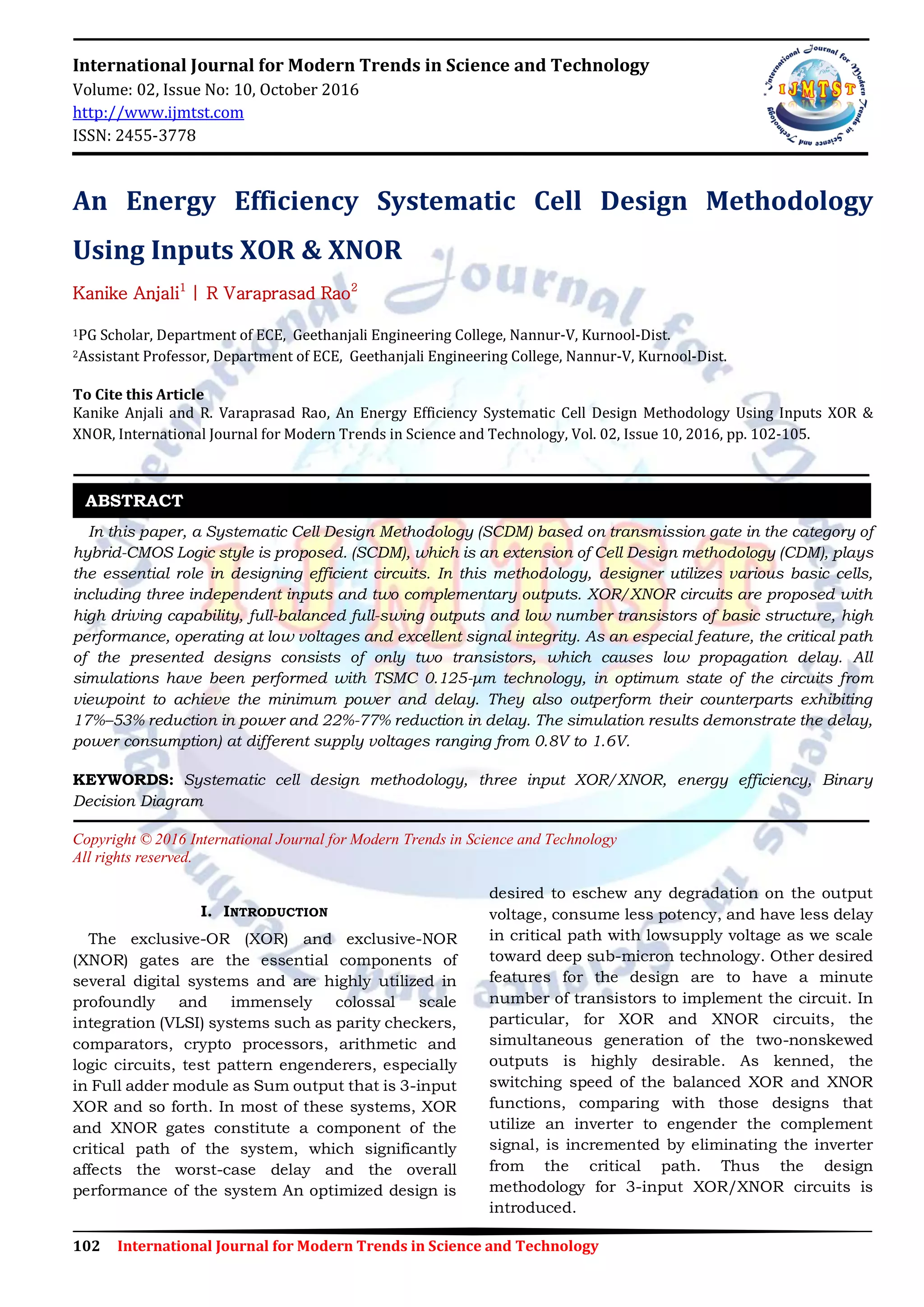
III. IMPLEMENTATION
14 Transistors adder cell need only 14
transistors to realize the full adder function. By
sacrificing four extra transistors per adder cell as
compared to SERF, it engenders the better result in
threshold loss, speed and potency. The threshold
loss quandary is reduced in this adder design,
which subsists in the SERF by inserting the
inverter between XOR Gate outputs which will
compose XNOR gate.. The design of 14 transistors
full adder utilizes 4 transistors XOR gate same as
SERF for its operation with supplemental inverter
circuit at the output of XOR gate in order to amend
the threshold loss quandary. Design of 4 transistor
XOR gate is shown in fig.6 In this XOR gate circuit,
when A=B=0, transistor P1 and P2 will be on and
Transistor N1 and N2 will be off. Consequently low
input at input B will pass through transistor P2
and we get low signal at the output. When A=0 and
B=1, transistor N1 and P2 will be on and Transistor
P1 and N2 will be off. Consequently high input at
input B will pass through transistor P2 and we get
high signal at the output.
Fig:-2 Circuit diagram for 4T XOR gate
When A=1 and B=0, transistor N2 and P1 will be
on and Transistor P2 and N1 will be off. At the
output we get high signal from Input A through
transistor P1 and N2. When A=1 and B=1,
transistor N1 and N2 will be on and transistor P1
and transistor P2 will be off, thus we get low signal
at the output. Circuit diagram for 14 transistor full
adder circuit using 4 transistor XOR gate.
Fig:-3 Circuit diagram for 14T full adder
IV. EXPERIMENTAL RESULTS
Fig:-4 Circuit
Fig:-5 Result](https://image.slidesharecdn.com/180ijmtst021055-161030064339/85/An-Energy-Efficiency-Systematic-Cell-Design-Methodology-Using-Inputs-XOR-XNOR-3-320.jpg)
![105 International Journal for Modern Trends in Science and Technology
Kanike Anjali and R. Varaprasad Rao : An Energy Efficiency Systematic Cell Design Methodology Using Inputs XOR
& XNOR
Fig:-6 Data Result
V. CONCLUSION
The performance of many more astronomically
immense circuits rudimentally depends upon the
performance of the full adder circuits that have
been utilized. So, the 14 transistor full adder
circuit is a good option to build the sizably
voluminous systems and circuits with low power
consumption and area. Predicated on analysis 14
transistor full adder has lesser delay, potency, area
and better precision. With the avail of this 14T
adder cell, we can design an efficient and high
performance multiplier unit. In future, this kind of
low power and high speed adder cell will be utilized
in designing the sundry digital circuits with lesser
area and hence less power and delay which is main
requisite of any digital circuit.
REFERENCES
[1] C.-H. Chang, J. Gu, and M. Zhang, “A review of
0.18-μm full adder performances for tree structured
arithmetic circuits,” IEEE Trans. Very Large Scale
Integr. (VLSI) Syst., vol. 13, no. 6, pp. 686–695, Jun.
2005.
[2] Goel, Ashok Kumar, M.A.Bayoumi, ”Design Of
Robust Energy Efficient Full Adders For Deep
Submicrometer Design Using Hybrid CMOS Logic
Style ”, IEEE Trans. Very Large Scale
Integr.(VLSI)Syst, December 2006.
[3] M. Aguirre-Hernandez and M. Linares-Aranda,
“CMOS full-adders for energy-efficient arithmetic
applications,” IEEE Trans. Very Large Scale Integr.
(VLSI) Syst., vol. 19,Apr. 2011.
[4] T. Nikoubin, A. Baniasadi, F. Eslami, and K. Navi, “A
new celld esign methodology for balanced
XOR-XNOR circuits for hybrid-CMOS logic,” J. Low
Power Electron., vol. 5, no. 4, pp. 474–483, 2009.
[5] T. Nikoubin, M. Grailoo, and S. H. Mozafari, “Cell
design methodology based on transmission gate for
low-power highspeed balanced XOR-XNOR circuits
in hybrid-CMOS logic style,” J. Low Power Electron.,
vol. 6, no. 4, pp. 503–512, 2010.
[6] Nikoubin, Tooraj, Mahdieh Grailoo, and Changzhi Li.
"Energy and Area Efficient Three-Input XOR/XNORs
With Systematic Cell Design Methodology." ,” IEEE
Trans. Very Large Scale Integr. (VLSI) Syst., vol.
24,January 2016](https://image.slidesharecdn.com/180ijmtst021055-161030064339/85/An-Energy-Efficiency-Systematic-Cell-Design-Methodology-Using-Inputs-XOR-XNOR-4-320.jpg)

This document presents a systematic cell design methodology for energy-efficient 3-input XOR/XNOR circuits using transmission gate technology. The proposed design achieves significant reductions in power consumption (17%-53%) and delay (22%-77%) compared to existing designs, while ensuring high driving capability and excellent signal integrity with minimal transistor count. Simulation results validate the methodology's effectiveness, demonstrating its potential for building efficient digital circuits with reduced area and power usage.