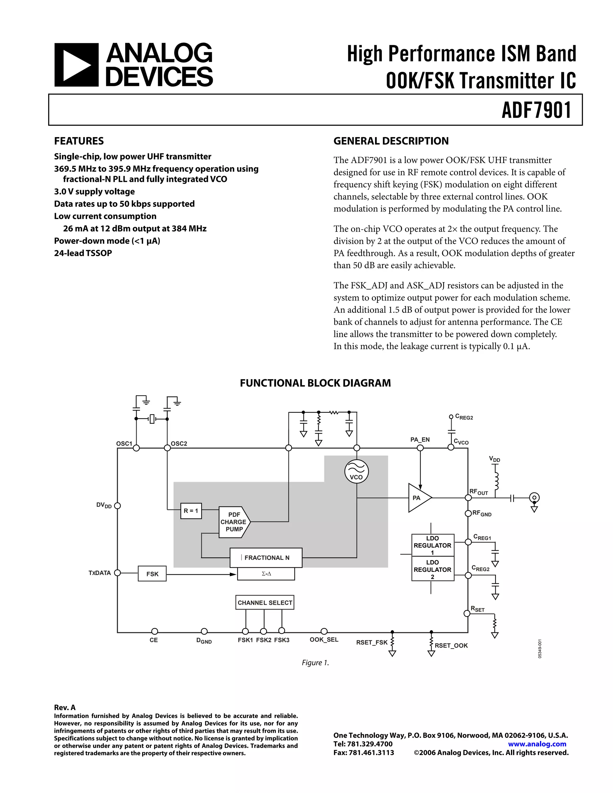
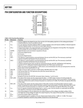
The ADF7901 is a low power UHF transmitter IC capable of OOK and FSK modulation up to 50 kbps. It operates from 369.5 MHz to 395.9 MHz using a fractional-N PLL and integrated VCO. The chip provides low current consumption of 26 mA at 12 dBm output and supports power-down mode below 1 μA. It allows selection of 8 channels for FSK modulation and provides over 50 dB modulation depth for OOK. External resistors set the output power levels for each modulation scheme.
![ADF7901
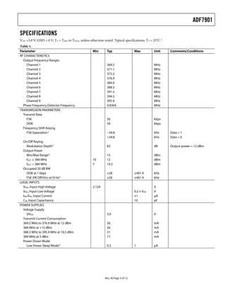
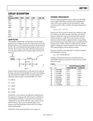
OUTLINE DIMENSIONS
7.90
7.80
7.70
24 13
4.50
4.40
4.30
6.40 BSC
1 12
PIN 1
0.65 1.20
BSC MAX
0.15
0.05
8° 0.75
0.30 0° 0.60
SEATING 0.20
0.19 PLANE 0.45
0.09
0.10 COPLANARITY
COMPLIANT TO JEDEC STANDARDS MO-153AD
Figure 9. 24-Lead Thin Shrink Small Outline Package [TSSOP]
(RU-24)
Dimensions shown in millimeters
ORDERING GUIDE
Model Temperature Range Package Description Package Option
ADF7901BRU 0°C to 50°C 24-Lead Thin Shrink Small Outline Package (TSSOP) RU-24
ADF7901BRU-REEL 0°C to 50°C 24-Lead Thin Shrink Small Outline Package (TSSOP) RU-24
ADF7901BRU-REEL7 0°C to 50°C 24-Lead Thin Shrink Small Outline Package (TSSOP) RU-24
ADF7901BRUZ 1 0°C to 50°C 24-Lead Thin Shrink Small Outline Package (TSSOP) RU-24
ADF7901BRUZ-RL1 0°C to 50°C 24-Lead Thin Shrink Small Outline Package (TSSOP) RU-24
ADF7901BRUZ-RL71 0°C to 50°C 24-Lead Thin Shrink Small Outline Package (TSSOP) RU-24
EVAL-ADF7901EB Evaluation Board
1
Z = Pb-free part.
Rev. A| Page 11 of 12](https://image.slidesharecdn.com/adf7901-121206031905-phpapp02/85/Adf7901-11-320.jpg)