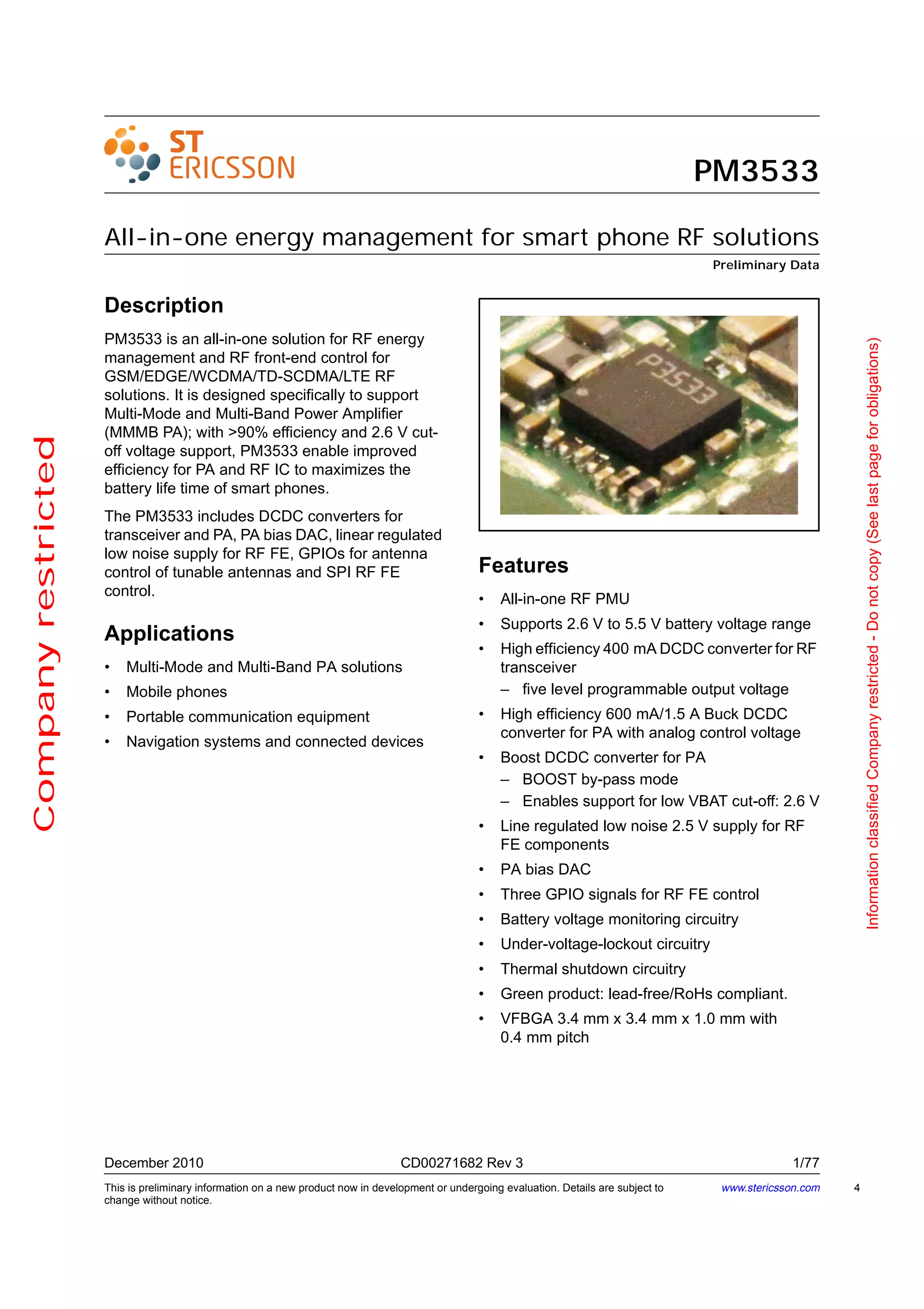
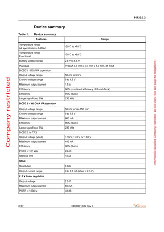
PM3533 is an all-in-one energy management solution for RF components in smartphones. It includes DC-DC converters to efficiently power the RF transceiver and power amplifier, a PA bias DAC, and voltage regulation to maximize battery life. The PM3533 supports multi-band and multi-mode phones with a battery voltage range of 2.6V to 5.5V and high efficiency power conversion. It allows for improved power efficiency and extended use of smartphones.
![List of tables PM3533
List of tables
Table 1. Device summary . . . . . . . . . . . . . . . . . . . . . . . . . . . . . . . . . . . . . . . . . . . . . . . . . . . . . . . . . . 2
Table 2. Absolute maximum ratings . . . . . . . . . . . . . . . . . . . . . . . . . . . . . . . . . . . . . . . . . . . . . . . . . 14
Table 3. Operation conditions . . . . . . . . . . . . . . . . . . . . . . . . . . . . . . . . . . . . . . . . . . . . . . . . . . . . . . 14
Table 4. Electrical characteristics of SMPS full power mode . . . . . . . . . . . . . . . . . . . . . . . . . . . . . . 19
Table 5. Electrical characteristics of SMPS section mode . . . . . . . . . . . . . . . . . . . . . . . . . . . . . . . . 20
Table 6. SMPS operation parameters . . . . . . . . . . . . . . . . . . . . . . . . . . . . . . . . . . . . . . . . . . . . . . . 21
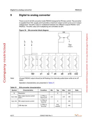
Table 7. SMPS inductor specification . . . . . . . . . . . . . . . . . . . . . . . . . . . . . . . . . . . . . . . . . . . . . . . . 25
Information classified Company restricted - Do not copy (See last page for obligations)
Table 8. SMPS capacitor specification . . . . . . . . . . . . . . . . . . . . . . . . . . . . . . . . . . . . . . . . . . . . . . . 26
Table 9. SMPS performance with critical components . . . . . . . . . . . . . . . . . . . . . . . . . . . . . . . . . . . 26
Table 10. Boost full power mode general electrical characteristics . . . . . . . . . . . . . . . . . . . . . . . . . . 27
Table 11. Boost converter operation parameters . . . . . . . . . . . . . . . . . . . . . . . . . . . . . . . . . . . . . . . . 28
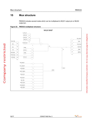
Table 12. Inductor specification . . . . . . . . . . . . . . . . . . . . . . . . . . . . . . . . . . . . . . . . . . . . . . . . . . . . . 31
Company restricted
Table 13. Capacitor specification for Boost converter . . . . . . . . . . . . . . . . . . . . . . . . . . . . . . . . . . . . 32
Table 14. DC-DC closed-loop mode electrical characteristics . . . . . . . . . . . . . . . . . . . . . . . . . . . . . . 33
Table 15. Buck DC-DC converter operating parameters . . . . . . . . . . . . . . . . . . . . . . . . . . . . . . . . . . 34
Table 16. Inductor specification for closed-loop mode DC-DC converter usage . . . . . . . . . . . . . . . . 38
Table 17. Capacitor specification for closed-loop mode DC-DC converter usage . . . . . . . . . . . . . . . 38
Table 18. Current output capability / nominal voltage. . . . . . . . . . . . . . . . . . . . . . . . . . . . . . . . . . . . . 39
Table 19. Regulator specifications . . . . . . . . . . . . . . . . . . . . . . . . . . . . . . . . . . . . . . . . . . . . . . . . . . . 39
Table 20. Power-up timing values . . . . . . . . . . . . . . . . . . . . . . . . . . . . . . . . . . . . . . . . . . . . . . . . . . . 41
Table 21. D/A-converter characteristics . . . . . . . . . . . . . . . . . . . . . . . . . . . . . . . . . . . . . . . . . . . . . . . 42
Table 22. PADAC coding table by setting ‘48’ [in dec] for fused values . . . . . . . . . . . . . . . . . . . . . . . 43
Table 23. I/O pad accuracy. . . . . . . . . . . . . . . . . . . . . . . . . . . . . . . . . . . . . . . . . . . . . . . . . . . . . . . . . 44
Table 24. RF control voltage output parameters . . . . . . . . . . . . . . . . . . . . . . . . . . . . . . . . . . . . . . . . 45
Table 25. Thermal shutdown parameter table . . . . . . . . . . . . . . . . . . . . . . . . . . . . . . . . . . . . . . . . . . 46
Table 26. Battery monitoring characteristics. . . . . . . . . . . . . . . . . . . . . . . . . . . . . . . . . . . . . . . . . . . . 48
Table 27. Under Voltage Lockout characteristics . . . . . . . . . . . . . . . . . . . . . . . . . . . . . . . . . . . . . . . . 49
Table 28. MUX1 register writings . . . . . . . . . . . . . . . . . . . . . . . . . . . . . . . . . . . . . . . . . . . . . . . . . . . . 51
Table 29. PM3533 Kelvin nodes for self test purpose . . . . . . . . . . . . . . . . . . . . . . . . . . . . . . . . . . . . 52
Table 30. Power up timing values. . . . . . . . . . . . . . . . . . . . . . . . . . . . . . . . . . . . . . . . . . . . . . . . . . . . 53
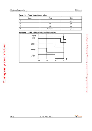
Table 31. Power down timing values . . . . . . . . . . . . . . . . . . . . . . . . . . . . . . . . . . . . . . . . . . . . . . . . . 54
Table 32. Data interface timings . . . . . . . . . . . . . . . . . . . . . . . . . . . . . . . . . . . . . . . . . . . . . . . . . . . . . 55
Table 33. SPI control signal timing table . . . . . . . . . . . . . . . . . . . . . . . . . . . . . . . . . . . . . . . . . . . . . . 56
Table 34. PM3533 pin description . . . . . . . . . . . . . . . . . . . . . . . . . . . . . . . . . . . . . . . . . . . . . . . . . . . 58
Table 35. Register 0 . . . . . . . . . . . . . . . . . . . . . . . . . . . . . . . . . . . . . . . . . . . . . . . . . . . . . . . . . . . . . . 61
Table 36. Register 1 . . . . . . . . . . . . . . . . . . . . . . . . . . . . . . . . . . . . . . . . . . . . . . . . . . . . . . . . . . . . . . 61
Table 37. Register 2 . . . . . . . . . . . . . . . . . . . . . . . . . . . . . . . . . . . . . . . . . . . . . . . . . . . . . . . . . . . . . . 62
Table 38. Register 3 . . . . . . . . . . . . . . . . . . . . . . . . . . . . . . . . . . . . . . . . . . . . . . . . . . . . . . . . . . . . . . 63
Table 39. Register 4 . . . . . . . . . . . . . . . . . . . . . . . . . . . . . . . . . . . . . . . . . . . . . . . . . . . . . . . . . . . . . . 64
Table 40. Register 5 . . . . . . . . . . . . . . . . . . . . . . . . . . . . . . . . . . . . . . . . . . . . . . . . . . . . . . . . . . . . . . 65
Table 41. Register 6 . . . . . . . . . . . . . . . . . . . . . . . . . . . . . . . . . . . . . . . . . . . . . . . . . . . . . . . . . . . . . . 65
Table 42. Register 7 . . . . . . . . . . . . . . . . . . . . . . . . . . . . . . . . . . . . . . . . . . . . . . . . . . . . . . . . . . . . . . 66
Table 43. Register 8 . . . . . . . . . . . . . . . . . . . . . . . . . . . . . . . . . . . . . . . . . . . . . . . . . . . . . . . . . . . . . . 67
Table 44. Register 9 . . . . . . . . . . . . . . . . . . . . . . . . . . . . . . . . . . . . . . . . . . . . . . . . . . . . . . . . . . . . . . 68
Table 45. Register 12 . . . . . . . . . . . . . . . . . . . . . . . . . . . . . . . . . . . . . . . . . . . . . . . . . . . . . . . . . . . . . 68
Table 46. Register 13 . . . . . . . . . . . . . . . . . . . . . . . . . . . . . . . . . . . . . . . . . . . . . . . . . . . . . . . . . . . . . 69
Table 47. Register 14 . . . . . . . . . . . . . . . . . . . . . . . . . . . . . . . . . . . . . . . . . . . . . . . . . . . . . . . . . . . . . 69
Table 48. Register 15 . . . . . . . . . . . . . . . . . . . . . . . . . . . . . . . . . . . . . . . . . . . . . . . . . . . . . . . . . . . . . 70
8/77 CD00271682 Rev 3](https://image.slidesharecdn.com/cd00271682pm3533datasheetrev31968-111011021759-phpapp01/85/CD00271682_PM3533_datasheet_rev3-8-320.jpg)
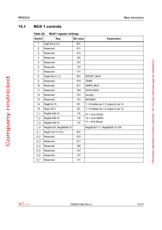
![PM3533 SMPS for PA
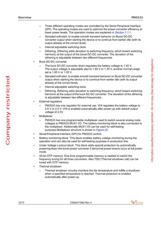
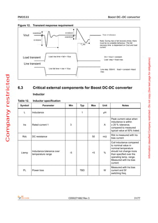
5.3 Operating parameters for SMPS converter
Characteristics to be met over the operating temperature range specified in Table 3:
Operation conditions unless otherwise stated.
Table 6. SMPS operation parameters
Symbol Parameter Min Typ Max Unit Notes
Voltage levels and regulation
Operating input voltage Accuracy: +/- 3%
Vi_oper1 5.82 6 6.18 V
Information classified Company restricted - Do not copy (See last page for obligations)
(full power mode) BOOST OUTPUT
Operating input voltage Accuracy: +/- 3%
Vi_oper2 5.15 5.3 5.45 V
(full power mode) BOOST OUTPUT
Operating input voltage Accuracy: +/- 3%
Vi_oper3 3.88 4 4.12 V
Company restricted
(full power mode) BOOST OUTPUT
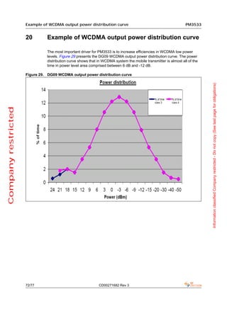
Operating input voltage Accuracy: +/- 3%
Vi_oper4 4.18 4.3 4.42 V
(full power mode) BOOST OUTPUT
Lowest power levels
Boost-converter is in by-
Operating input voltage Vbat min pass mode when SMPS
Vi_oper_low Vbat min V
(low power mode) - 350 mV input voltage is VBAT.
NOTE: Depends on the
application usage
smps_ctrl at (default gain setting)
0.023 0.066 0.073 0.080 Accuracy: +10.0/- 9.5%
0.03 0.088 0.095 0.103 Accuracy: +8.0/- 7.9%
0.1 0.326 0.318 0.311 Accuracy: +2.6/- 2.3%
0.4 1.269 1.272 1.277 Accuracy: +0.4/-0.2%
Vout
0.75 2.385 V (used as a ratio reference)
-[-30;+85]°C
1.00 3.195 3.243 Accuracy: +0.2/+0.05%
1.25 3.982 4.001 Accuracy: +0.65/+0.2%
1.55 4.964 5.097 Accuracy: +3.4/+0.7%
1.59 5.097 5.446 Accuracy: +7.7/+0.8%
1.62 5.198 5.461 Accuracy: +6.0/+0.9%
Look at smps_ctrl = 0.75V /
g1 3.18
Gain, Vout Vout = 2.385V above
g2 3.38 Optional (via bit control)
Iload=1.25A @Vi_oper2
Dropout Switching freq 9.5 MHz.
Included LC DCR/ACR
voltage at room Note: Minimum delay setting 370 420 mV
temp used @ Vi_oper2. values (see Section 5.4
values)
Iload=1.25A @Vi_oper2
Dropout
Switching frequency typ of Included LC DCR/ACR
voltage 270 350 mV
5.0 MHz @ Vi_oper2. (1) values (see Section 5.4
-[-30;+85]°C
values)
CD00271682 Rev 3 21/77](https://image.slidesharecdn.com/cd00271682pm3533datasheetrev31968-111011021759-phpapp01/85/CD00271682_PM3533_datasheet_rev3-21-320.jpg)
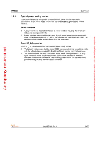
![SMPS for PA PM3533
Table 6. SMPS operation parameters (continued)
Symbol Parameter Min Typ Max Unit Notes
@Vout max= 4.7 V
Note: Max currents are
Iload Load current 1.2 1.7 A defined during the GSM
burst. MAX value includes
PA current consumption in
worst case VSWR case.
Load current in GSM mode @Vout max= 3.6 V
when Boost-converter is by-
Information classified Company restricted - Do not copy (See last page for obligations)
Note: Max currents are
Iload_mode passed or PA max power is 2.5 A
defined during the GSM
achieved lower than
nominal SMPS Vout value. burst.
Note: PA is in power-down
mode.
Company restricted
No load current Includes internal clock and
Inol drivers and internal
consumption 3 3.5 mA
-[-30;+85]°C regulator quiescent
Switching freq 9.5MHz currents.
Converter in full power
mode
Note: PA is in power-down
mode and PM3533 is in
Iidle
Idle current 0.6 0.8 mA idle mode.
-[-30;+85]°C
Regulators are on.
Clock and drivers are off.
Clock range can be tuned with 5+
1-bit
6.5 13.5
Adjustable Internal clock (with the 1stset of reduction /
f_osc (4.7/7.9) (11.7 /14.9) MHz
increment bits)
(typical values) [2.1/5.3] [8.2/10.5]
[with the 2nd set of reduction /
increment bits]
7.1 10.0 Tuning range over temp, vbat and
f_osc_tuning_ corners.
[5.7, [9.3,
range OTP tuning range MHz [extended range available
4.2, 5.8,
dedicated control bits:
-[-30;+85]°C 3.3] 5.45] set 1, set2, set3]
f_osc_tuning_ Can be tuned with OTP
memory and with 4+1-bit
acc 160 230 350 kHz
current bias. Absolute
-[-30;+85]°C
accuracy.
Delta
Tuned OTP freq shift over
f_osc_shift 450 ΔkHz
vbat and temp.
-[-30;+85]°C
f_osc_d1 Selectable 2MHz dither
Dither deviation 1 1.9 2 MHz
-[-30;+85]°C deviation
f_osc_d2 Selectable 4MHz dither
Dither deviation 2 3.7 4 MHz
-[-30;+85]°C deviation
Vin 300mVpp perturbation.
Line_tr (2) Line transient response mVpp Trise/tfall=10 µs.
Iload = 1.25 A DC
22/77 CD00271682 Rev 3](https://image.slidesharecdn.com/cd00271682pm3533datasheetrev31968-111011021759-phpapp01/85/CD00271682_PM3533_datasheet_rev3-22-320.jpg)
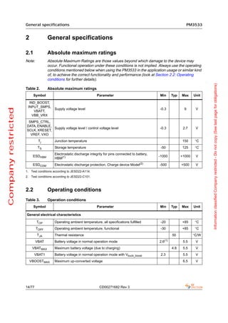
![PM3533 SMPS for PA
Table 6. SMPS operation parameters (continued)
Symbol Parameter Min Typ Max Unit Notes
Vin=Vbat range
Transients from 10 mA to
Load_tr (2) Load transient response (3)
mVpp
1250 mA.
Trise = Tfall = 13 µs.
PSRR sine wave perturbation
Mode1 Iout = 1200 mA 35 dB
[-30;+85]°C <10 kHz
Information classified Company restricted - Do not copy (See last page for obligations)
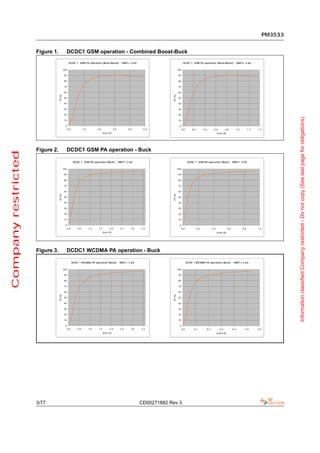
Efficiency in GSM-mode
Vin = 5 V. Iload 1.25 A @ Iload = 1.25A (GSM burst
[-30;+85]°C Vout, typ = 4.6 V 93 95 % rms current value). Full
Switching freq 9.5 MHz power mode
Company restricted
Vin = 3.6 V. Iload 0.52A @ SMPS full power mode,.
[-30;+85]°C Vout = 2 V, 89 92 % Boost converter by-passed
Switching freq 9.5 MHz (active mode)
Vin = 3.6 V. Iload 0.17 A @ SMPS Section mode,.
[-30;+85]°C Vout = 1.1 V, 79 83 % Boost converter by-passed
Switching freq 9.5 MHz (active mode)
Vin = 5.0 V. Iload 0.52 A @
SMPS full power mode in
[-30;+85]°C Vout = 2 V, 87.5 90.5 %
VUSB case
Switching freq 9.5 MHz
Vin = 5.0 V. Iload 0.17 A @
Vout = 1.1 V, SMPS section mode in
[-30;+85]°C 74 77 %
VUSB case
Switching freq 9.5 MHz
Efficiency in WCDMA-mode
Vin = 3.6 V. Iload 0.5 A @ SMPS Section power
[-30;+85]°C Vout, typ = 3.37 V 93 94.5 % mode, Boost by-passed
Switching freq 2.1 MHZ (active mode)
Vin = 3.6 V. Iload 0.15 @ SMPS section mode,
[-30;+85]°C Vout = 1.6V, 85 88 % Boost by-passed (passive
Switching freq 2.1 MHZ mode)
Vin = 3. 6V. Iload 0.045 @ SMPS section mode,
[-30;+85]°C Vout = 0.77 V, 62 68 % Boost by-passed (passive
Switching freq 2.1 MHZ mode) (4)
Vin = 5.0 V. Iload 0.5 A @
Vout, typ = 3.37 V SMPS section power mode
[-30;+85]°C 92 93.5 %
in VUSB case
Switching freq 2.1 MHZ
Vin = 5.0 V. Iload 0.15 @
SMPS section mode in
[-30;+85]°C Vout = 1.6V, 81 84 %
VUSB case
Switching freq 2.1 MHZ
Vin = 5.0 V. Iload 0.045 @
SMPS section mode in
[-30;+85]°C Vout = 0.77 V, 56 62 %
VUSB case
Switching freq 2.1 MHZ
CD00271682 Rev 3 23/77](https://image.slidesharecdn.com/cd00271682pm3533datasheetrev31968-111011021759-phpapp01/85/CD00271682_PM3533_datasheet_rev3-23-320.jpg)
![PM3533 Boost DC-DC converter
Table 11. Boost converter operation parameters (continued)
Symbol Parameter Min Typ Max Unit Remarks
Note: PA is in power-down mode and
PM3533 is thus in idle mode
Quiescent current (no (i.e.SMPS_ctrl=0V).
Iq1 load) Full power mode 14 26 mA Includes internal clock & control blocks
Switching freq 7 MHz and boost trap capacitor circuitry & power
stages, and also internal regulator
quiescent currents
Adjustable Internal
Information classified Company restricted - Do not copy (See last page for obligations)
f_osc 4.5 11.4 MHz Clock range can be tuned with 5-bit
clock (typical values)
f_osc_tuning
Tuning range over temp, vbat and
_range OTP tuning range 6.8 8.0 MHz
corners.
[30; +85°C]
Company restricted
f_osc_tuning
Can be tuned with OTP memory and with
_acc 160 220 330 kHz
4-bit current bias. Absolute accuracy.
[30; +85°C]
Delta
f_osc_shift 450 ΔkHz Tuned OTP freq shift over vbat and temp.
[-30; +85°C]
f_osc_d1
Dither deviation1 1.9 2 MHz Selectable 2 MHz dither deviation
[-30; +85°C]
f_osc_d2
Dither deviation2 3.7 4 MHz Selectable 4 MHz dither deviation
[-30; +85°C]
Vin 300 mVpk perturbation.
Line_tr(1) Line transient (2) Trise/tfall=10 µs. Iload = 1200 mA.
mVpp
[-30; +85°C] response(1). In the application SMPS and BOOST
blocks are in series.
Vin= 3.6 V
Load_tr Load transient
250 mVpp Transients from 10 mA to 1250 mA
[-30; +85°C] response(1)
Trise = Tfall = 13.3 µs.
Line_tr
Line regulation(1). 0.1 0.2 mV Vin 2.7 – 5.3V, Iload 1200 mA
[-30; +85°C]
Load_tr Iload 10 mA – 1200 mA, Vin 5 V,
Load regulation(1) 20 mV
[-30; +85°C] Vin 2.7 V
PSRR Mode Boost+ SMPS
35 dB sine wave perturbation <10 kHz
[-30; +85°C] Iout = 1250 mA
Efficiency - condition Vbat = 3.6 V
Vbatt = 3.6 V
Iload 1.2 A
η @ Vout = 5.3 V, 89 92 % Boost in full power mode
switching freq 7 MHz
over full Temp. range
CD00271682 Rev 3 29/77](https://image.slidesharecdn.com/cd00271682pm3533datasheetrev31968-111011021759-phpapp01/85/CD00271682_PM3533_datasheet_rev3-29-320.jpg)
![PM3533 BUCK DC-DC converter
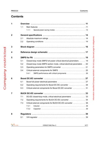
7 BUCK DC-DC converter
The BUCK DC-DC-converter design topology used is similar to the SMPS one. DC-DC-
converter control is performed via the reference voltage.
Figure 13. Buck DC-DC-converter simplified block diagram
Information classified Company restricted - Do not copy (See last page for obligations)
Company restricted
7.1 DC-DC closed-loop mode, critical electrical parameters
The most critical parameters are collected in Table 14.
Table 14. DC-DC closed-loop mode electrical characteristics
Symbol Parameter Min Typ Max Unit
VBAT Input voltage range 2.3 4.4 V
Vout1 Output voltage, programmable 1.35 V
Vout2 Output voltage, programmable 1.45 V
Vout3 Output voltage, programmable 1.65 V
Vout4 Output voltage, programmable 1.55 V
Vout5 Output voltage, programmable 1.85 V
Iout Output current range 400 mA
Active current consumption (no load
Iq 3.5 4.5 mA
current (1);
Efficiency with 100mA load
[-30;+85]°C VBAT 3.6V, switching freq 2.1 MHz, 87 88 %
Vout 1.45 V (coil 3u3, case 2520)
CD00271682 Rev 3 33/77](https://image.slidesharecdn.com/cd00271682pm3533datasheetrev31968-111011021759-phpapp01/85/CD00271682_PM3533_datasheet_rev3-33-320.jpg)
![BUCK DC-DC converter PM3533
Table 14. DC-DC closed-loop mode electrical characteristics (continued)
Symbol Parameter Min Typ Max Unit
Efficiency with 150mA load
[-30;+85]°C VBAT 3.6V, switching freq 2.1 MHz, 89 90 %
Vout 1.45 V (coil 3u3, case 2520)
Efficiency with 200mA load
[-30;+85]°C VBAT 3.6V, switching freq 2.1 MHz, 89 90 %
Vout 1.45 V (coil 3u3, case 2520)
Efficiency with 300mA load
Information classified Company restricted - Do not copy (See last page for obligations)
[-30;+85]°C VBAT 3.6V, switching freq 2.1 MHz, 88 89.5 %
Vout 1.45 V (coil 3u3, case 2520)
Max continuous load current 400 mA
Programmable switching frequency
1.8 4.5 MHz
Company restricted
(5-bit)
Startup time (function of load LC
10(2) µs
circuitry)
1. In the continuous conduction mode of coil current
2. For example, C=10 µF, L=2.2 µH
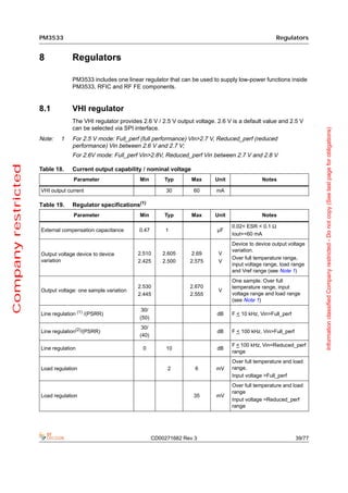
7.2 Operating requirements for BUCK DC-DC converter
The following characteristics are to be met over the operating temperature range specified
in Table 3: Operation conditions, unless otherwise stated.
Table 15. Buck DC-DC converter operating parameters
Symbol Parameter Min Typ Max Unit Notes
Voltage levels and regulation
Operating input
Vi_oper 2.3 4.4 V
voltage
Accuracy +/- 3%. Including
Output voltage 1) 1.309 1.350 1.390 V ripple voltage and line/load
Output voltage 2) 1.406 1.450 1.493 V regulation.
Vout1,2,3,4,5 Output voltage 3) 1.600 1.650 1.699 V Output voltage can be
Output voltage 4) 1.504 1.550 1.596 V programmed based on
Output voltage 5) 1.795 1.850 1.905 V battery voltage information
from base band.
Reference voltage External band-gap
Vref 1.182 1.200 1.218 V
accuracy reference voltage
RF IC is also included in
Iload Load current 10 400 mA
maximum Iload
Max. Iload and VBAT at
2.7 V
Ibatt VBAT input current 250 mA
Note: 1.45 V output
voltage used.
34/77 CD00271682 Rev 3](https://image.slidesharecdn.com/cd00271682pm3533datasheetrev31968-111011021759-phpapp01/85/CD00271682_PM3533_datasheet_rev3-34-320.jpg)
![PM3533 BUCK DC-DC converter
Table 15. Buck DC-DC converter operating parameters (continued)
Symbol Parameter Min Typ Max Unit Notes
Note: the RF IC is in
power-down mode and
PM3533 is in idle mode.
Quiescent current
(no load) Includes internal clock &
Iq 3.5 4.5 mA control blocks and boost
Switching frequency
trap capacitor
2 MHz
circuitry/power stages.Also
internal regulator
Information classified Company restricted - Do not copy (See last page for obligations)
quiescent currents.
Adjustable Internal Clock range can be tuned
f_osc 1.8 4.5 MHz
clock (typical values) with 5-bit
f_osc_
Tuning range over temp,
tuning_range OTP tuning range 2.5 2.8 MHz
Company restricted
vbat and corners.
[-30;+85]°C
f_osc_tuning_ Can be tuned with OTP
memory and with 4-bit
acc 60 120 kHz
current bias. Absolute
-[-30;+85]°C
accuracy.
Delta
f_osc_shift Tuned OTP freq shift over
250 kHz
vbat and temp.
-[-30;+85]°C
f_osc_d1 Selectable 1 MHz dither
Dither deviation1 0.8 1 MHz
-[-30;+85]°C deviation
f_osc_d2 Selectable 2 MHz dither
Dither deviation2 1.8 2 MHz
-[-30;+85]°C deviation
Vin 300 mVpk
Line_tr Line transient perturbation.
2 4 mVpp
Figure 14 response. Trise/tfall=10 µs
Iload = 400 mA.
Vin=2.3/3.6/ 4.4 V
Load_tr
Load transient Transients from 10 mA to
[-30;+85]°C 10 20 mVpp
response 400 mA
Figure 14
Trise = Tfall = 10 µs.
Line_tr
Vin 2.3 V – 4.4 V,
[-30;+85]°C Line regulation. 0.1 0.2 mV
Iload 400 mA
Figure 14
Load_tr
Iload 10 mA – 400 mA,
[-30;+85]°C Load regulation 1 2 mV
Vin 4.4 V, Vin 2.3 V
Figure 14
PSRR Mode1 sine wave perturbation
58 dB
[-30;+85]°C Iout = 400mA <10 kHz
CD00271682 Rev 3 35/77](https://image.slidesharecdn.com/cd00271682pm3533datasheetrev31968-111011021759-phpapp01/85/CD00271682_PM3533_datasheet_rev3-35-320.jpg)
![BUCK DC-DC converter PM3533
Table 15. Buck DC-DC converter operating parameters (continued)
Symbol Parameter Min Typ Max Unit Notes
Efficiency measured with coil 3u3 case2520, condition: Vbat 3.6 V closed-loop mode
Vin = 3.6 V.
Iload 300 mA
DC-DC in normal power
[-30;+85]°C @ Vout = 1.45 V 88 89.5 %
mode
Switching freq.
2.1MHz
Vin = 3.6 V.
Information classified Company restricted - Do not copy (See last page for obligations)
Iload 200 mA
DC-DC in normal power
[-30;+85]°C @ Vout = 1.45V 89 90 %
mode
Switching freq
2.1MHz
Vin = 3.6 V.
Company restricted
Iload 150 mA
DC-DC in normal power
[-30;+85]°C @ Vout = 1.45 V 89 90 %
mode
Switching freq
2.1MHz
Vin = 3.6 V.
Iload 100 mA
DC-DC in normal power
[-30;+85]°C @ Vout = 1.45 V 87 88 %
mode
Switching freq
2.1 MHz
Vin = 3.6 V.
Iload 60 mA
DC-DC in normal power
[-30;+85]°C @ Vout = 1.45 V 82 84 %
mode
Switching freq
2.1 MHz
Efficiency measured with coil 3u3 case2520, condition: VUSB 5.0 V closed-loop mode
Vbatt =5.0 V.
Iload 300 mA
Buck DC-DC in VUSB
[-30;+85]°C @ Vout = 1.45 V 86.5 88 %
case
Switching freq.
2.1MHz
Vin = 5.0 V.
Iload 200 mA
Buck DC-DC in VUSB
[-30;+85]°C @ Vout = 1.45V 87 89 %
case
Switching freq
2.1MHz
Vin = 5.0 V.
Iload 150 mA
Buck DC-DC in VUSB
[-30;+85]°C @ Vout = 1.45 V 86 87 %
case
Switching freq
2.1MHz
Vin = 5.0 V.
Iload 100 mA
Buck DC-DC in VUSB
[-30;+85]°C @ Vout = 1.45 V 83 84 %
case
Switching freq
2.1 MHz
36/77 CD00271682 Rev 3](https://image.slidesharecdn.com/cd00271682pm3533datasheetrev31968-111011021759-phpapp01/85/CD00271682_PM3533_datasheet_rev3-36-320.jpg)
![PM3533 BUCK DC-DC converter
Table 15. Buck DC-DC converter operating parameters (continued)
Symbol Parameter Min Typ Max Unit Notes
Vin = 5.0 V.
Iload 60 mA
Buck DC-DC in VUSB
[-30;+85]°C @ Vout = 1.45 V 77 79 %
case
Switching freq
2.1 MHz
Timing (refer to start-up and mode change section)
Initial condition:
Information classified Company restricted - Do not copy (See last page for obligations)
t_idle_dcdc Regulators on DC-DC-
Idle to operation
6 12 μs converter off, output
[-30;+85]°C Sampled soft-start
capacitor charged but not
loaded.
Power-off to
T_on_dcdc
Company restricted
DC-DC-converter power-
operation 35 55 μs
[-30;+85]°C up, output at 0V.
Sampled soft-start
Figure 14. Transient response requirement
tr<XXmV
overshoot
Vout Vout +/-tolerance
overshoot
tr<XXmV Note: During rise or fall recovery times,
there must be no unstable behaviour.
T_rec The fall recovery time is dependant on
Cout and load current
Load transient Load rise time = fall = 10us Vin = Vout = constant.
Load step = Iload max.
Line transient Line fall time = rise = 10us Line step: 300mV. Iload = constant
= Ilaod max
CD00271682 Rev 3 37/77](https://image.slidesharecdn.com/cd00271682pm3533datasheetrev31968-111011021759-phpapp01/85/CD00271682_PM3533_datasheet_rev3-37-320.jpg)
![PM3533 Digital to analog converter
Table 21. D/A-converter characteristics (continued)
Symbol Characteristics Condition Min Typ Max Unit Note
Monotonic
behavior
INL1 Integral non-linearity 1.5 LSB
required @
VHI = 2.5 V
Monotonic
behavior
INL2 Integral non-linearity 0.9 LSB
required @
VHI = 2.6 V
Information classified Company restricted - Do not copy (See last page for obligations)
DNL Differential non-linearity 0.5 LSB
Maximum output voltage 2.2 V
DAC output voltage in PD 100 mV
Company restricted
Internal mux switch
Mux_res (use external resistor of 47ohm 35 55 mΩ
to get max of 100ohm as worst
case)
In addition to normal usage of the current mode PADAC it is possible to use extra added
feature in order to use a coded output current to have a better accuracy of PADAC output
current. During a mass-production phase and its OTP fusing phase PADAC output current
by a certain code of 48 [in dec] is read/saved to certain register bits so this information can
be taken into use by combining dedicated bits. Look at the register table in the end part of
this datasheet for further details of registers available.
The application sw is able to read these dedicated bits in the following way:
After a normal power-up, read reg15.bit_numbers of [10,5,0] + reg2.bit[7] = MSB…LSB
order of bits for saved value and by looking at the accurate measured output current
value like it is coded in the table below.
Table 22. PADAC coding table by setting ‘48’ [in dec] for fused values
Coded value [in decimal] Corresponding value [mA]
0 1.600
1 1.645
2 1.690
3 1.735
4 1.780
5 1.825
6 1.870
7 1.915
8 1.960
9 2.005
10 2.050
11 2.095
CD00271682 Rev 3 43/77](https://image.slidesharecdn.com/cd00271682pm3533datasheetrev31968-111011021759-phpapp01/85/CD00271682_PM3533_datasheet_rev3-43-320.jpg)
![Digital to analog converter PM3533
Table 22. PADAC coding table by setting ‘48’ [in dec] for fused values
Coded value [in decimal] Corresponding value [mA]
12 2.140
13 2.185
14 2.230
15 2.275
The following kind of an accuracy can be achieved through setting of reg9.bits[15...9] i.e.
‘1100001’ which equals to 48 [in dec] + enable_bit_of_padac. This setting is used while the
Information classified Company restricted - Do not copy (See last page for obligations)
coded value is saved like informed for corresponding output current values in the table
above, thus being saved during the fusing phase of the mass-production testing
Table 23. I/O pad accuracy
Company restricted
I/O PAD Parameter Min Typ Max Unit
PADAC1 or
Accuracy by ‘1100001’- value -50 +50 μΑ
PADAC2
Then it is straightforward to use this information like matching a linear equation with the
following characteristic equation:
PADAC_output_current(Padac_output_code_wanted)
= (y_offset / (48 - 1)) * (Padac_output_code_wanted - 1) + min_LSB_size
In which
min_LSB_size = 33uA
y_offset = Coded_value - min_LSB_size
* Coded_value (in μA) is read from the table PADAC coding table
With this added feature the following kind of an accuracy of
PADAC_output_current (Padac_output_code_wanted)
can be achieved as a function of different PADAC control bits in Reg9[15...10]:
Figure 17. Output current accuracy of PADAC coded characteristic equation
44/77 CD00271682 Rev 3](https://image.slidesharecdn.com/cd00271682pm3533datasheetrev31968-111011021759-phpapp01/85/CD00271682_PM3533_datasheet_rev3-44-320.jpg)
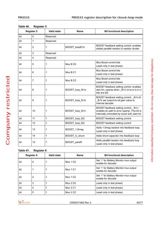
![PM3533 register description for closed-loop mode PM3533
Table 36. Register 1 (continued)
Register 1 Valid state Name Bit functional description
Enables functional measurement in test
bit 6 1 ENa_TEMP
mode
TSD_temp_ctrl => 00 150C;10 140C; 01
bit 7 1 TSD_fuse1
160C; 11 170C (used in test mode)
TSD_temp_ctrl => 00 150C;10 140C; 01
bit 8 1 TSD_fuse0
160C; 11 170C (used in test mode)
bit 9 1 Mux_VREG_ctrl_C2 (used only in test phase)
Information classified Company restricted - Do not copy (See last page for obligations)
bit 10 1 Mux_VREG_ctrl_C1 (used only in test phase)
bit 11 1 Mux_VREG_ctrl_C0 (used only in test phase)
bit 12 1 Mux_HV_ctrl C2 (used only in test phase)
Company restricted
bit 13 1 Mux_HV_ctrl C1 (used only in test phase)
bit 14 1 Mux_HV ctrl_C0 (used only in test phase)
bit 15 1 OTP_prog_ena Enables OTP signal paths in test phase
Table 37. Register 2
Register2 Valid state Name Bit functional description
Internal AFForce_bit[15].Frequency
bit 0 1 AFForce_bit[15]; RETKU reduction enable; 1.79MHz minus offset to
the SMPS value in register 14.
Internal AFForce_bit[16].Frequency
bit 1 1 AFForce_bit[16]; ITKU increasing enable; 1.35MHz plus offset to
the SMPS value in register 14.
bit 2 1 AFForce_bit[17] Internal AFForce_bit[17]
bit 3 1 AFForce_bit[18] Internal AFForce_bit[18]
bit 4 1 AFForce_bit[19] Internal AFForce_bit[19]
FuseData[15]; Programmed OTP RETKU
bit 5 read only FuseData[15]
bit. To read it keep reg15.bit='0'.
FuseData[16]; Programmed OTP ITKU bit.
bit 6 read only FuseData[16]
To read it keep reg15.bit='0'.
FuseData[39]. This is used for in serial
read-out of OTP memory. Keep
FuseData[39]/AFForce_bit[ reg14.bit15='0' to see this serial clocked
bit 7 read only data stream output i.e. D39.
17]
PADAC coded bit number 0 (LSB), others
look at register 15.
FuseData[18]. Programmed THSD Fuse0
bit 8 read only FuseData[18]
bit. To read it keep reg15.bit='0'.
FuseData[19]. Lower OTP mem MSB bit.
bit 9 read only FuseData[19] Programmed THSD Fuse1 bit. To read it
keep reg15.bit='0'.
62/77 CD00271682 Rev 3](https://image.slidesharecdn.com/cd00271682pm3533datasheetrev31968-111011021759-phpapp01/85/CD00271682_PM3533_datasheet_rev3-62-320.jpg)
![PM3533 PM3533 register description for closed-loop mode
Table 37. Register 2
Register2 Valid state Name Bit functional description
‘0' for enable sr_latch to output tsd_out
bit 10 0/1 tsd_mux1_ena state in pwmreg1.bit15; '1' reset sr_latch
output node to low state in pwmreg1.bit15.
In test mode smps rds_on low/high side
bit 11 0/1 rds_smps_low_high_ena sw can be set; '0' for low side; '1' for high
side
In test mode boost rds_on low/high side
Information classified Company restricted - Do not copy (See last page for obligations)
bit 12 0/1 rds_boost_low_high_ena sw can be set; '0' for low side; '1' for high
side
In test mode dcdc rds_on low/high side sw
bit 13 0/1 rds_dcdc_low_high_ena
can be set; '0' for low side; '1' for high side
In test_mode: '1'->'0' sequence to
bit 14 0/1 test_otp_reset
Company restricted
manually set otp_reset_pulse for OTP_cell
SMPS: the 5th delay tune for very high
bit 15 1 long_delay load impedances; when used set
reg3.bit[3...0]='1000'
Table 38. Register 3
Register3 Valid state Name Bit functional description
Delay tune for low side of driver chain;
bit 0 1 SMPS_ast_l beneficial for having minimum dropout
voltage (used ext coil res affects)
Delay tune for low side of driver chain;
bit 1 1 SMPS_ast_l beneficial at larger range of power levels
(GSM)
Delay tune for low side of driver chain;
beneficial at larger range of power level
bit 2 1 SMPS_ast_l
(GSM) but with larger dropout voltage
(used ext coil res affects)
Delay tune for low side of driver chain;
bit 3 1 SMPS_ast_l beneficial mid-to-low-power range loads
(WCDMA)
bit 4 1 Dither bandwidth 0 for 2.8MHz; 1 for 5.6MHz
bit 5 1 SMPS_Dither_ena SMPS dither enable
bit 6 1 SMPS_drw_inout SMPS drw in/out enable
SMPS_CTRL_bias/comp/ Enable for smps_ctrl bias. Enable for
bit 7 1
sawt smps_ctrl comparator/sawtooth
SMPS mode selection 00=PD, 01=bypass,
10=section, 11 normal (bits as bit '9', bit '8'
bit 8 1 SMPS mode selection
order) Cdoup_SMPS is enabled also with
01=bypass
bit 9 1 SMPS mode selection (used with bit 8)
CD00271682 Rev 3 63/77](https://image.slidesharecdn.com/cd00271682pm3533datasheetrev31968-111011021759-phpapp01/85/CD00271682_PM3533_datasheet_rev3-63-320.jpg)
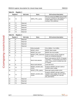
![PM3533 register description for closed-loop mode PM3533
Table 41. Register 6 (continued)
Register 6 Valid state Name Bit functional description
bit 6 1 Batman_ENA Enable control for Batman_out
('0' for res_div (set bit8 to '0'); '1' for
bit 7 1 Batman_KelvinH
res_meas (set bit8 to '0'); test structures)
('0' for res_div (set bit7 to '0'); '1' for hi-Z
bit 8 1 Batman_KelvinL
state (set bit7 to '1'); test structures)
(‘00’ = PD, '10'=DC-DC_clock '01' =
bit 9 1 Clock divider enable SMPS_CLOCK, 11 = Boost_clock (bits
Information classified Company restricted - Do not copy (See last page for obligations)
9,10 order); used only in test phase)
bit 10 1 Clock divider enable (used only in test phase)
Enabling digital buffers for ANT_T1,
ANT_T2, RFCTRL3 I/Os,
Company restricted
1= Digital buffers enabled in application
ANT_T1_T2_RFCTRL3_
bit 11 1 mode,
ctrl
0= OTP_clock @ANT_T1 and
TSD_testsense @ANT_T2 enabled in test
mode.
Enable switch for RFCTRL3, 1=digital high
bit 12 1 RFCTRL3_set
state, 0=digital low_state
ANTENNA tuning switch control, 1=digital
bit 13 1 ANT_T1_antsw_set
high state, 0=digital low_state
ANTENNA tuning switch control, 1=digital
bit 14 1 ANT_T2_antsw_set
high state, 0=digital low_state
(0 = mux outputs 8- 13,
bit 15 1 MUX switch
1 = mux outputs 1-7; used in test phase)
Table 42. Register 7
Register 7 Valid state Name Bit functional description
SMPS feedback setting control: linked to
0x5C01 setting (and alternatively 0x5C0D
with reg2.bit0=’1’ and reg14.bit15=’1’ for
bit 0 1 SMPS_loop_fb3 lowest switching freq), additionally 0x5C05
or 0x5C09 (=recommended) with
reg2.bit0='1' and reg14.bit15='1' for the
semi-lowest switching frequency
Enables open loop gain increment option
bit 1 1 Open_gain_inc
(especially in EER/ET architecture)
Additional smps freq reduction (bits of
[3...2] combines 4 selections); can be used
bit 2 1 Freq_red1
in GSM/WCDMA (in OTP or in free-
running OSC modes)
Additional smps freq reduction (bits of
[3...2] combines 4 selections); can be used
bit 3 1 Freq_red2
in GSM/WCDMA (in OTP or in free-
running OSC modes)
66/77 CD00271682 Rev 3](https://image.slidesharecdn.com/cd00271682pm3533datasheetrev31968-111011021759-phpapp01/85/CD00271682_PM3533_datasheet_rev3-66-320.jpg)
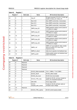
![PM3533 register description for closed-loop mode PM3533
Table 43. Register 8 (continued)
Register 8 Valid state Name Bit functional description
Enable for DC-DC soft start; starts at
DCDC_ sampled output voltage; this bit is left for
bit 12 1
sampled_start_control sw compatibility (because it was like
fast_start before)
bit 13 1 DC-DCmux (DC-DC mux C0; used in test phase)
bit 14 1 DC-DCmux (DC-DC mux C1; used in test phase)
bit 15 1 DC-DCmux (DC-DC mux C2; used in test phase)
Information classified Company restricted - Do not copy (See last page for obligations)
Table 44. Register 9
Register 9 Valid state Name Bit functional description
bit 0 1 DC-DC_loop_fb1 DC-DC feedback setting control
Company restricted
bit 1 1 DC-DC_loop_fb1 DC-DC feedback setting control
bit 2 1 DC-DC_loop_fb1 DC-DC feedback setting control
bit 3 1 DC-DC_loop_fb2 DC-DC feedback setting control
bit 4 1 DC-DC_loop_fb2 DC-DC feedback setting control
bit 5 Reserved
bit 6 1 DC-DC_C_shunt Adds shunt capacitor into feedback loop
(Adds parallel resistor into feedback loop;
bit 7 1 DC-DC_paraR
used only in test phase)
(Enables 2.5V @Vref=1.2V; normally not
bit 8 1 OVER2VENA used in the closed-loop configuration of
SMPS usage in the rf subsystem)
bit 9 1 PA_DAC_XPD Enable for PA_DAC
bit 10 1 PA_DAC bit0 PA DAC control
bit 11 1 PA_DAC bit1 PA DAC control
bit 12 1 PA_DAC bit2 PA DAC control
bit 13 1 PA_DAC bit3 PA DAC control
bit 14 1 PA_DAC bit4 PA DAC control
bit 15 1 PA_DAC bit5 PA DAC control
Table 45. Register 12
Register 12 Valid state Name Bit functional description
bit 0 read only FuseDR[0] FuseDR[0] (Upper OTP mem LSB bit)
bit 1 read only FuseDR[1] FuseDR[1]
bit 2 read only FuseDR[2] FuseDR[2]
bit 3 read only FuseDR[3] FuseDR[3]
bit 4 read only FuseDR[4] FuseDR[4]
bit 5 read only FuseDR[5] FuseDR[5]
68/77 CD00271682 Rev 3](https://image.slidesharecdn.com/cd00271682pm3533datasheetrev31968-111011021759-phpapp01/85/CD00271682_PM3533_datasheet_rev3-68-320.jpg)
![PM3533 PM3533 register description for closed-loop mode
Table 45. Register 12
Register 12 Valid state Name Bit functional description
bit 6 read only FuseDR[6] FuseDR[6]
bit 7 read only FuseDR[7] FuseDR[7]
bit 8 read only FuseDR[8] FuseDR[8]
bit 9 read only FuseDR[9] FuseDR[9]
bit 10 read only FuseDR[10] FuseDR[10]
bit 11 read only FuseDR[11] FuseDR[11]
Information classified Company restricted - Do not copy (See last page for obligations)
bit 12 read only FuseDR[12] FuseDR[12]
bit 13 read only FuseDR[13] FuseDR[13]
bit 14 read only FuseDR[14] FuseDR[14]
Company restricted
bit 15 read only FuseDR[15] FuseDR[15]
Table 46. Register 13
Register 13 Valid state Name Bit functional description
bit 0 read only FuseDR[16] FuseDR[16]
bit 1 read only FuseDR[17] FuseDR[17]
bit 2 read only FuseDR[18] FuseDR[18]
bit 3 read only FuseDR[19] FuseDR[19] (Upper OTP mem MSB bit)
bit 4 read only Version_bit0 Coding of versions as follows (bit3...bit0)
PM3533: ‘001’ for v1.0
bit 5 read only Version_bit1
PM3533: ‘010’ for v1.0B
bit 6 read only Version_bit2
bit 7 read only Version_bit3
bit 8 read only Family_bit0 Coding of RF PM IC family
bit 9 read only Family_bit1 PM3533: ‘010’
bit 10 read only Family_bit2
bit 11 read only Man_bit0 Coding of RF PM IC manufacturer
bit 12 read only Man_bit1 PM3533: ‘111’
bit 13 read only Man_bit2
bit 14 Reserved
bit 15 Reserved
Table 47. Register 14
Register 14 Valid state Name Bit functional description
These bits adjust switching frequency so
bit 0 1 SMPS_clock_freq
that bits 00000 gives minimum freq
bit 1 1 SMPS_clock_freq and 11111 gives max freq.
CD00271682 Rev 3 69/77](https://image.slidesharecdn.com/cd00271682pm3533datasheetrev31968-111011021759-phpapp01/85/CD00271682_PM3533_datasheet_rev3-69-320.jpg)
![PM3533 register description for closed-loop mode PM3533
Table 47. Register 14
Register 14 Valid state Name Bit functional description
For SMPS: '00000': 6.48 MHz; '01101':
bit 2 1 SMPS_clock_freq
9.54 MHz; '01110': 9.77 MHz;
bit 3 1 SMPS_clock_freq '11111': 13.59 MHz (typical values)
(SMPS: Calibration range in the OTP used
bit 4 1 SMPS_clock_freq mode is 7.1 - 10.1 MHz when
reg7.bit[3...2]=’00’)
These bits adjust switching frequency so
Information classified Company restricted - Do not copy (See last page for obligations)
bit 5 1 BOOST_clock_freq
that bits 00000 gives minimum freq
bit 6 1 BOOST_clock_freq and 11111 gives max freq.
For Boost: '00000': 4.51 MHz; '01101':
bit 7 1 BOOST_clock_freq
7.52 MHz; '01110': 7.74 MHz;
Company restricted
bit 8 1 BOOST_clock_freq '11111':11.42 MHz (typical values)
(Boost: Calibration range in the OTP used
bit 9 1 BOOST_clock_freq
mode is 6.8 - 8.0 MHz)
These bits adjust switching frequency so
bit 10 1 DC-DC_clock_freq
that bits 0000 gives minimum freq
bit 11 1 DC-DC_clock_freq and 1111 gives max freq.
For RF-IC DCDC: '00000': 1.62 MHz;
bit 12 1 DC-DC_clock_freq
'01110'': 2.75 MHz;
'01111':2.83 MHz; '11111': 4.09 MHz
bit 13 1 DC-DC_clock_freq
(typical values)
(DCDC: Calibration range in the OTP used
bit 14 1 DC-DC_clock_freq
mode is 2.45 - 2.84 MHz)
0' sets OTP mode which uses trimmed
bit 15 1 DATA_ENA
values; '1' is for user set values.
Table 48. Register 15
Reg 15 Valid state Name Bit functional description
FuseData[0] (Lower OTP mem LSB bit) /
bit 0 read only FuseData[0]
PADAC coded bit number 1
1 read only FuseData[1] FuseData[1]
2 read only FuseData[2] FuseData[2]
3 read only FuseData[3] FuseData[3]
4 read only FuseData[4] FuseData[4]
5 read only FuseData[5] FuseData[5] / PADAC coded bit number 2
6 read only FuseData[6] FuseData[6]
7 read only FuseData[7] FuseData[7]
8 read only FuseData[8] FuseData[8]
9 read only FuseData[9] FuseData[9]
70/77 CD00271682 Rev 3](https://image.slidesharecdn.com/cd00271682pm3533datasheetrev31968-111011021759-phpapp01/85/CD00271682_PM3533_datasheet_rev3-70-320.jpg)
![PM3533 PM3533 register description for closed-loop mode
Table 48. Register 15 (continued)
Reg 15 Valid state Name Bit functional description
FuseData[10] / PADAC coded bit number
10 read only FuseData[10]
3
11 read only FuseData[11] FuseData[11]
12 read only FuseData[12] FuseData[12]
13 read only FuseData[13] FuseData[13]
14 read only FuseData[14] FuseData[14] (bits[19...15] in Reg2)
Information classified Company restricted - Do not copy (See last page for obligations)
15 read only FUSE_OK Internal Fuse_ok
Company restricted
CD00271682 Rev 3 71/77](https://image.slidesharecdn.com/cd00271682pm3533datasheetrev31968-111011021759-phpapp01/85/CD00271682_PM3533_datasheet_rev3-71-320.jpg)