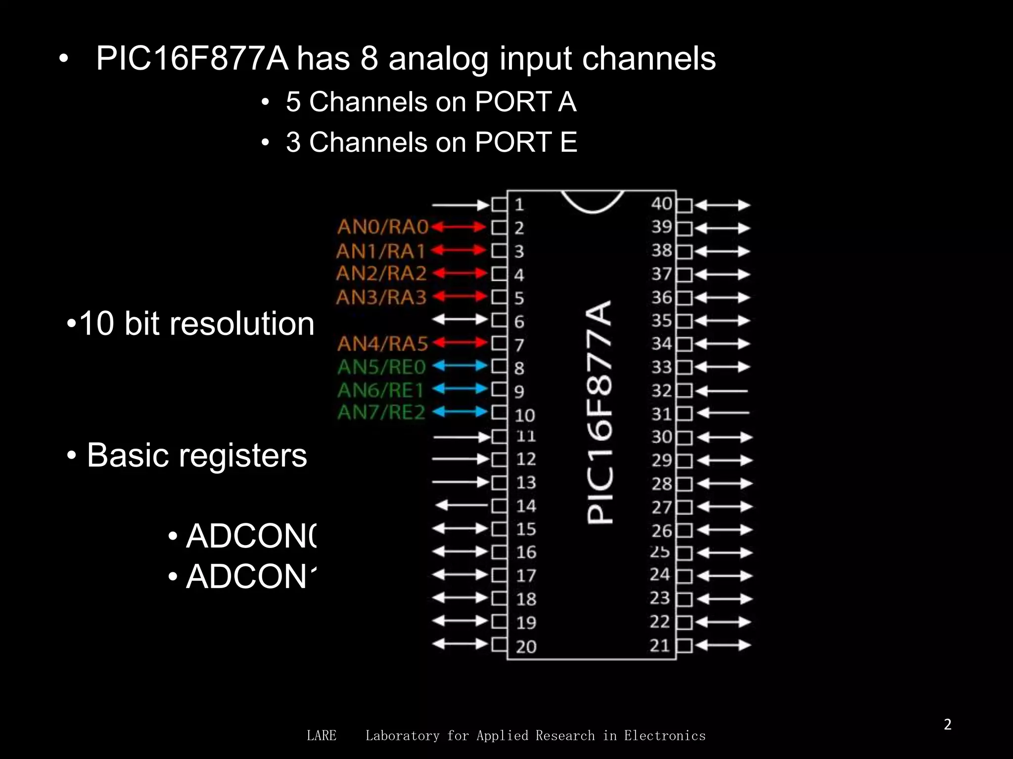
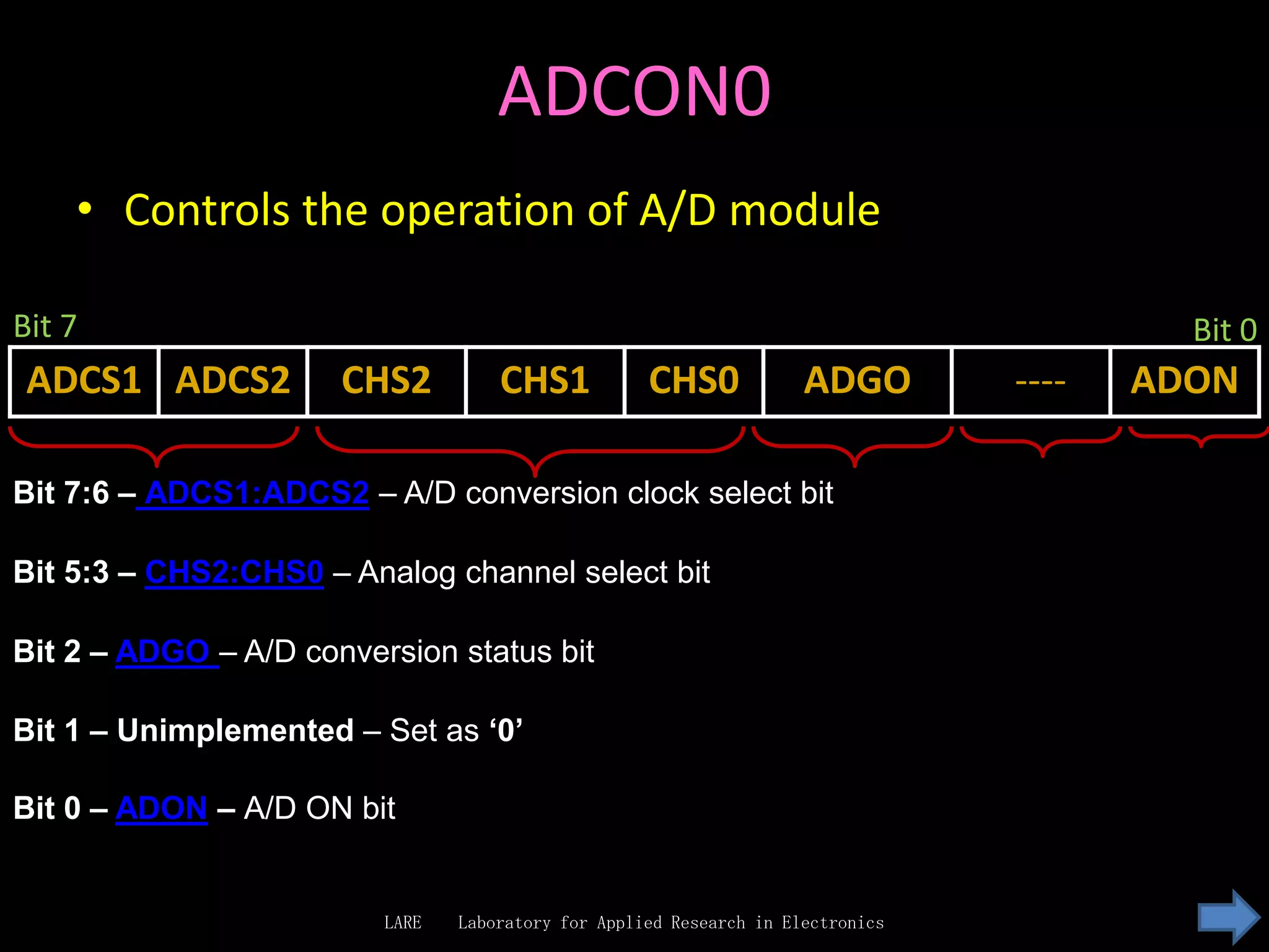
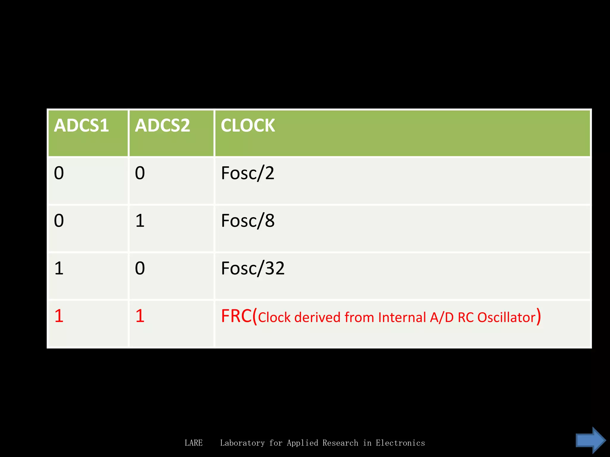
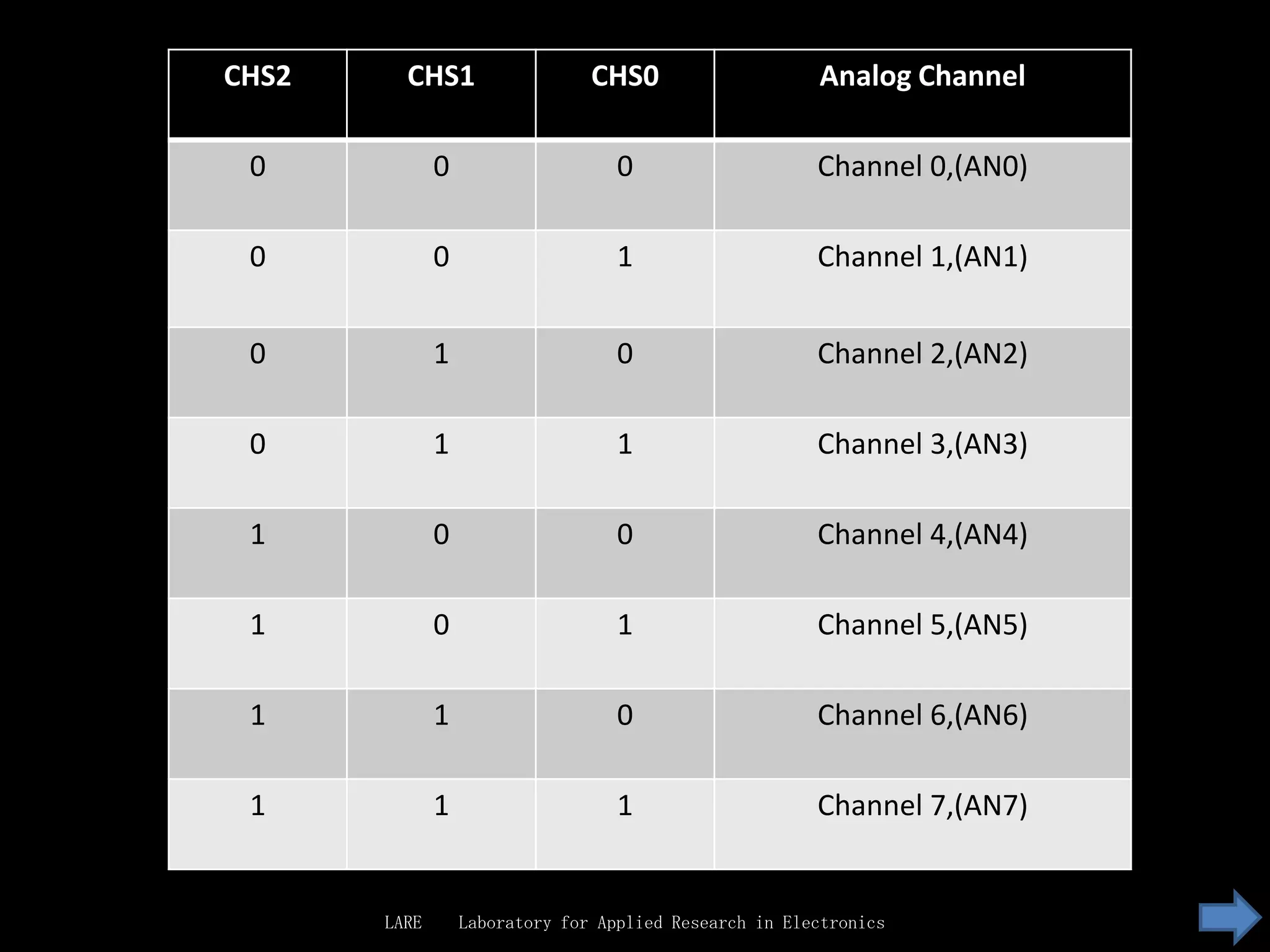
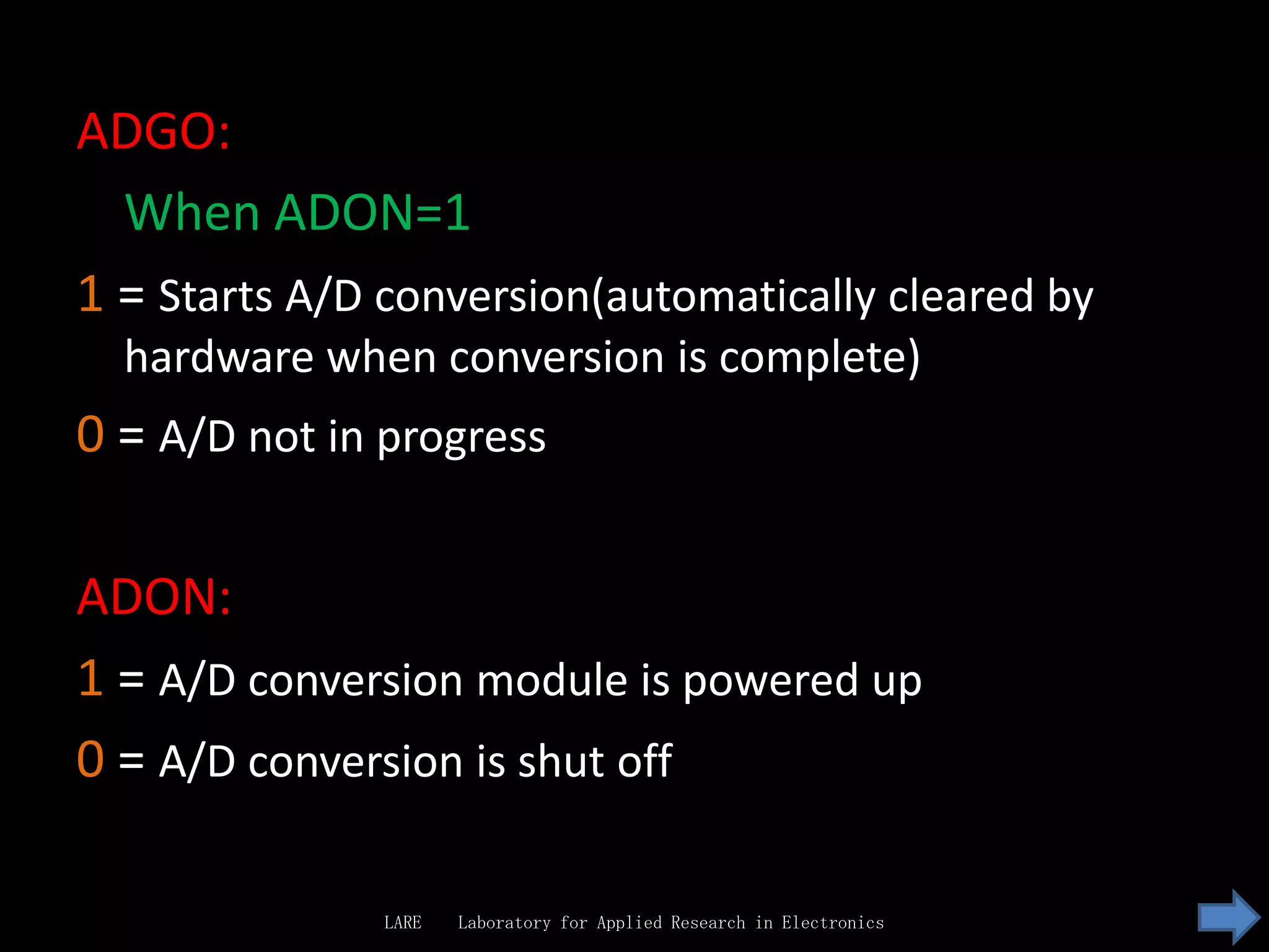
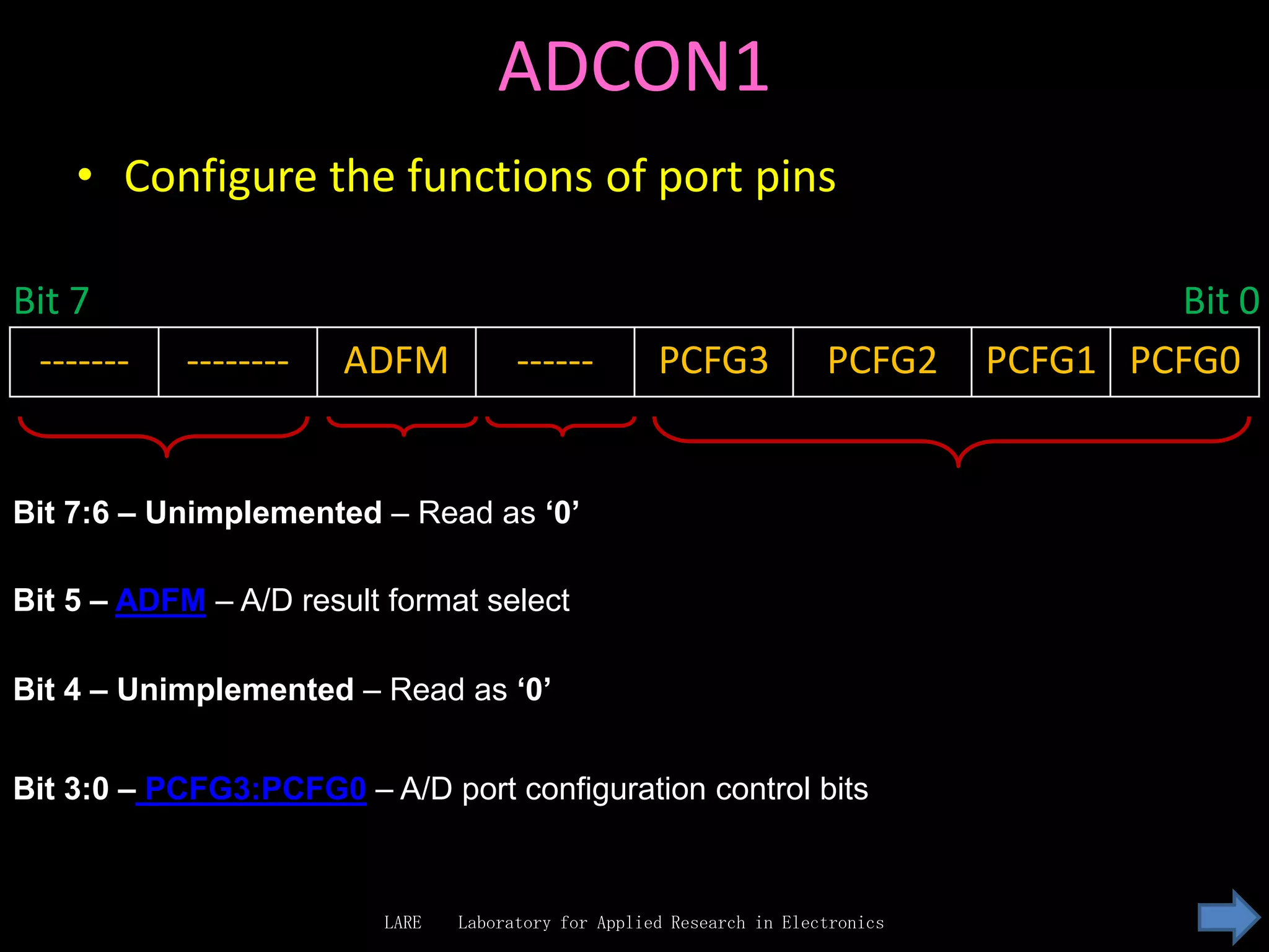
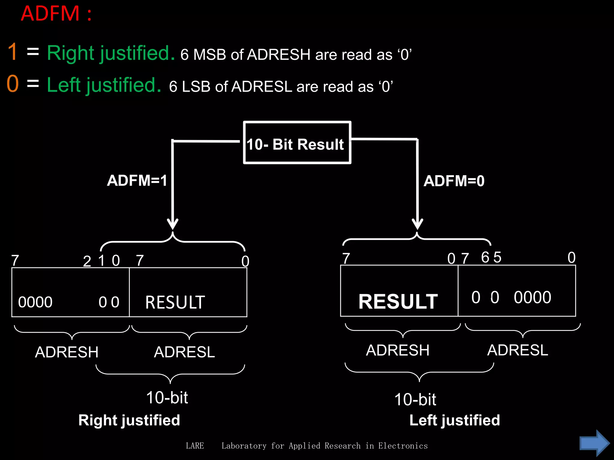
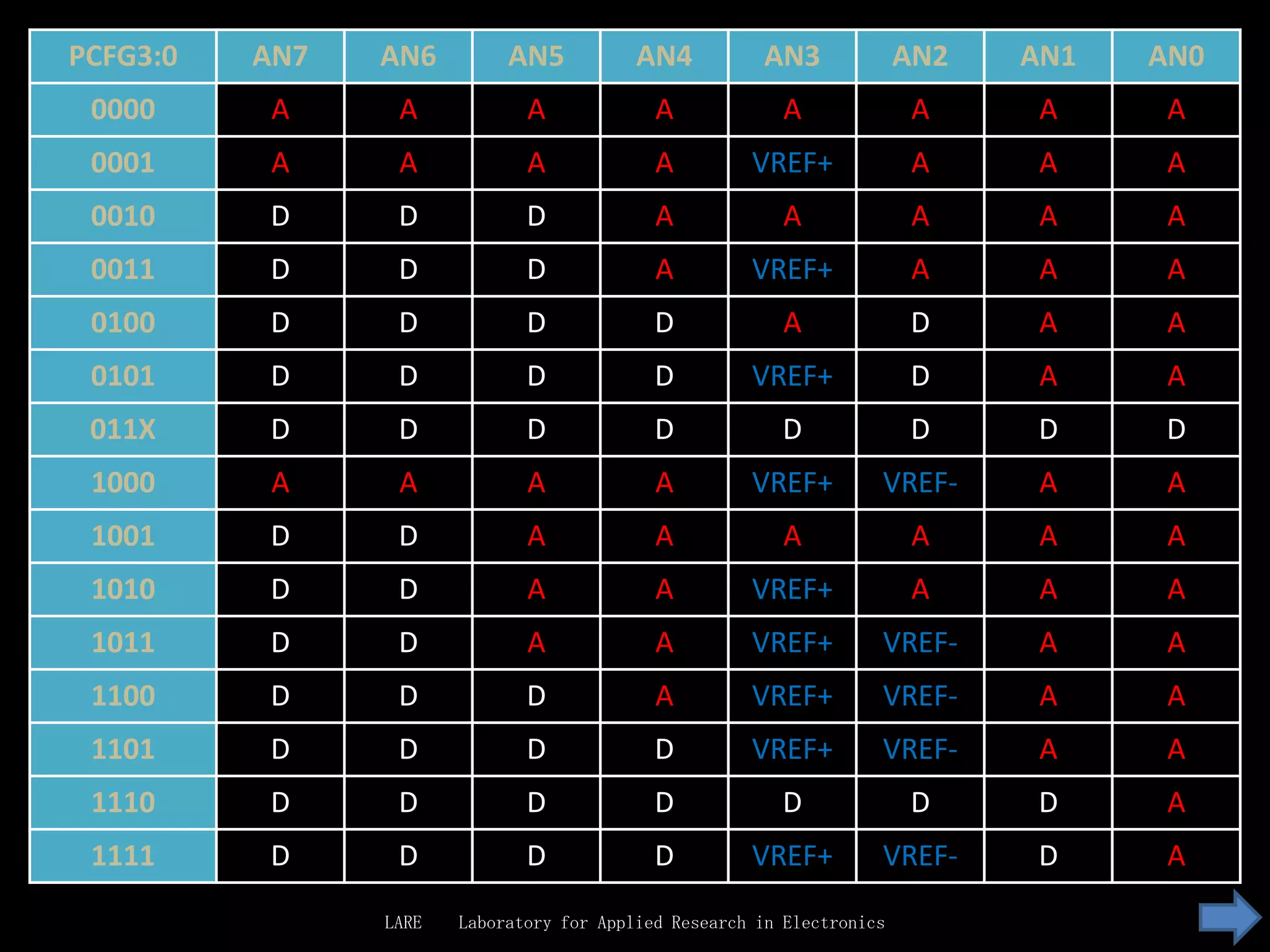
ADC


                                                        1
LARE   Laboratory for Applied Research in Electronics
• PIC16F877A has 8 analog input channels
              • 5 Channels on PORT A
              • 3 Channels on PORT E


•10 bit resolution


• Basic registers used for ADC conversion

       • ADCON0
       • ADCON1


                                                                         2
                 LARE   Laboratory for Applied Research in Electronics
ADCON0
    • Controls the operation of A/D module

Bit 7                                                                                     Bit 0
 ADCS1 ADCS2          CHS2          CHS1            CHS0             ADGO        ----   ADON

Bit 7:6 – ADCS1:ADCS2 – A/D conversion clock select bit

Bit 5:3 – CHS2:CHS0 – Analog channel select bit

Bit 2 – ADGO – A/D conversion status bit

Bit 1 – Unimplemented – Set as ‘0’

Bit 0 – ADON – A/D ON bit


                         LARE   Laboratory for Applied Research in Electronics
ADCS1   ADCS2      CLOCK

0       0          Fosc/2

0       1          Fosc/8

1       0          Fosc/32

1       1          FRC(Clock derived from Internal A/D RC Oscillator)


            LARE   Laboratory for Applied Research in Electronics
CHS2     CHS1                   CHS0                    Analog Channel

 0            0                    0                    Channel 0,(AN0)

 0            0                    1                    Channel 1,(AN1)


 0            1                    0                    Channel 2,(AN2)

 0            1                    1                    Channel 3,(AN3)

 1            0                    0                    Channel 4,(AN4)

 1            0                    1                    Channel 5,(AN5)

 1            1                    0                    Channel 6,(AN6)

 1            1                    1                    Channel 7,(AN7)


       LARE       Laboratory for Applied Research in Electronics
ADGO:
  When ADON=1
1 = Starts A/D conversion(automatically cleared by
  hardware when conversion is complete)
0 = A/D not in progress

ADON:
1 = A/D conversion module is powered up
0 = A/D conversion is shut off

               LARE   Laboratory for Applied Research in Electronics
ADCON1
    • Configure the functions of port pins

Bit 7                                                                                     Bit 0
 -------    --------   ADFM            ------         PCFG3             PCFG2     PCFG1 PCFG0


Bit 7:6 – Unimplemented – Read as ‘0’

Bit 5 – ADFM – A/D result format select

Bit 4 – Unimplemented – Read as ‘0’


Bit 3:0 – PCFG3:PCFG0 – A/D port configuration control bits


                          LARE   Laboratory for Applied Research in Electronics
ADFM :
1 = Right justified. 6 MSB of ADRESH are read as ‘0’
0 = Left justified. 6 LSB of ADRESL are read as ‘0’

                                       10- Bit Result

              ADFM=1                                                           ADFM=0


7        210      7                   0                     7                      0 7 65        0

 0000        00       RESULT                                    RESULT               0 0 0000


     ADRESH            ADRESL                                     ADRESH                ADRESL


                      10-bit                                            10-bit
         Right justified                                                   Left justified
                           LARE   Laboratory for Applied Research in Electronics
PCFG3:0   AN7   AN6         AN5           AN4          AN3              AN2   AN1   AN0
 0000      A     A            A             A             A              A     A     A
 0001      A     A            A             A         VREF+              A     A     A
 0010     D      D            D             A             A              A     A     A
 0011     D      D            D             A         VREF+              A     A     A
 0100     D      D            D             D             A             D      A     A
 0101     D      D            D             D         VREF+             D      A     A
 011X     D      D            D             D            D              D     D     D
 1000      A     A            A             A         VREF+         VREF-      A     A
 1001     D      D            A             A             A              A     A     A
 1010     D      D            A             A         VREF+              A     A     A
 1011     D      D            A             A         VREF+         VREF-      A     A
 1100     D      D            D             A         VREF+         VREF-      A     A
 1101     D      D            D             D         VREF+         VREF-      A     A
 1110     D      D            D             D            D              D     D      A
 1111     D      D            D             D         VREF+         VREF-     D      A
                LARE   Laboratory for Applied Research in Electronics

Adc(pic)

  • 1.
    ADC 1 LARE Laboratory for Applied Research in Electronics
  • 2.
    • PIC16F877A has8 analog input channels • 5 Channels on PORT A • 3 Channels on PORT E •10 bit resolution • Basic registers used for ADC conversion • ADCON0 • ADCON1 2 LARE Laboratory for Applied Research in Electronics
  • 3.
    ADCON0 • Controls the operation of A/D module Bit 7 Bit 0 ADCS1 ADCS2 CHS2 CHS1 CHS0 ADGO ---- ADON Bit 7:6 – ADCS1:ADCS2 – A/D conversion clock select bit Bit 5:3 – CHS2:CHS0 – Analog channel select bit Bit 2 – ADGO – A/D conversion status bit Bit 1 – Unimplemented – Set as ‘0’ Bit 0 – ADON – A/D ON bit LARE Laboratory for Applied Research in Electronics
  • 4.
    ADCS1 ADCS2 CLOCK 0 0 Fosc/2 0 1 Fosc/8 1 0 Fosc/32 1 1 FRC(Clock derived from Internal A/D RC Oscillator) LARE Laboratory for Applied Research in Electronics
  • 5.
    CHS2 CHS1 CHS0 Analog Channel 0 0 0 Channel 0,(AN0) 0 0 1 Channel 1,(AN1) 0 1 0 Channel 2,(AN2) 0 1 1 Channel 3,(AN3) 1 0 0 Channel 4,(AN4) 1 0 1 Channel 5,(AN5) 1 1 0 Channel 6,(AN6) 1 1 1 Channel 7,(AN7) LARE Laboratory for Applied Research in Electronics
  • 6.
    ADGO: WhenADON=1 1 = Starts A/D conversion(automatically cleared by hardware when conversion is complete) 0 = A/D not in progress ADON: 1 = A/D conversion module is powered up 0 = A/D conversion is shut off LARE Laboratory for Applied Research in Electronics
  • 7.
    ADCON1 • Configure the functions of port pins Bit 7 Bit 0 ------- -------- ADFM ------ PCFG3 PCFG2 PCFG1 PCFG0 Bit 7:6 – Unimplemented – Read as ‘0’ Bit 5 – ADFM – A/D result format select Bit 4 – Unimplemented – Read as ‘0’ Bit 3:0 – PCFG3:PCFG0 – A/D port configuration control bits LARE Laboratory for Applied Research in Electronics
  • 8.
    ADFM : 1 =Right justified. 6 MSB of ADRESH are read as ‘0’ 0 = Left justified. 6 LSB of ADRESL are read as ‘0’ 10- Bit Result ADFM=1 ADFM=0 7 210 7 0 7 0 7 65 0 0000 00 RESULT RESULT 0 0 0000 ADRESH ADRESL ADRESH ADRESL 10-bit 10-bit Right justified Left justified LARE Laboratory for Applied Research in Electronics
  • 9.
    PCFG3:0 AN7 AN6 AN5 AN4 AN3 AN2 AN1 AN0 0000 A A A A A A A A 0001 A A A A VREF+ A A A 0010 D D D A A A A A 0011 D D D A VREF+ A A A 0100 D D D D A D A A 0101 D D D D VREF+ D A A 011X D D D D D D D D 1000 A A A A VREF+ VREF- A A 1001 D D A A A A A A 1010 D D A A VREF+ A A A 1011 D D A A VREF+ VREF- A A 1100 D D D A VREF+ VREF- A A 1101 D D D D VREF+ VREF- A A 1110 D D D D D D D A 1111 D D D D VREF+ VREF- D A LARE Laboratory for Applied Research in Electronics