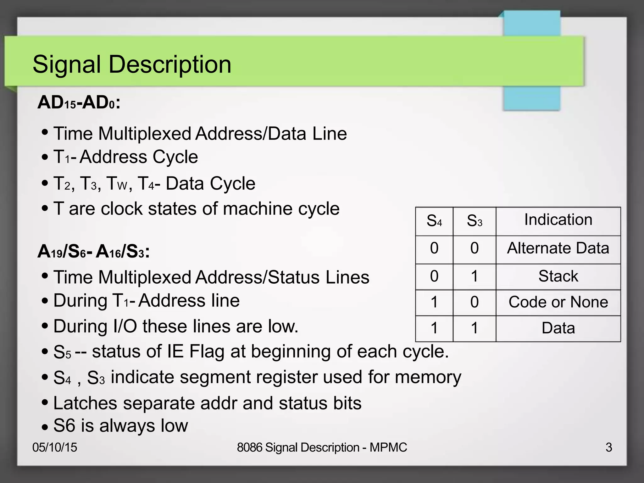
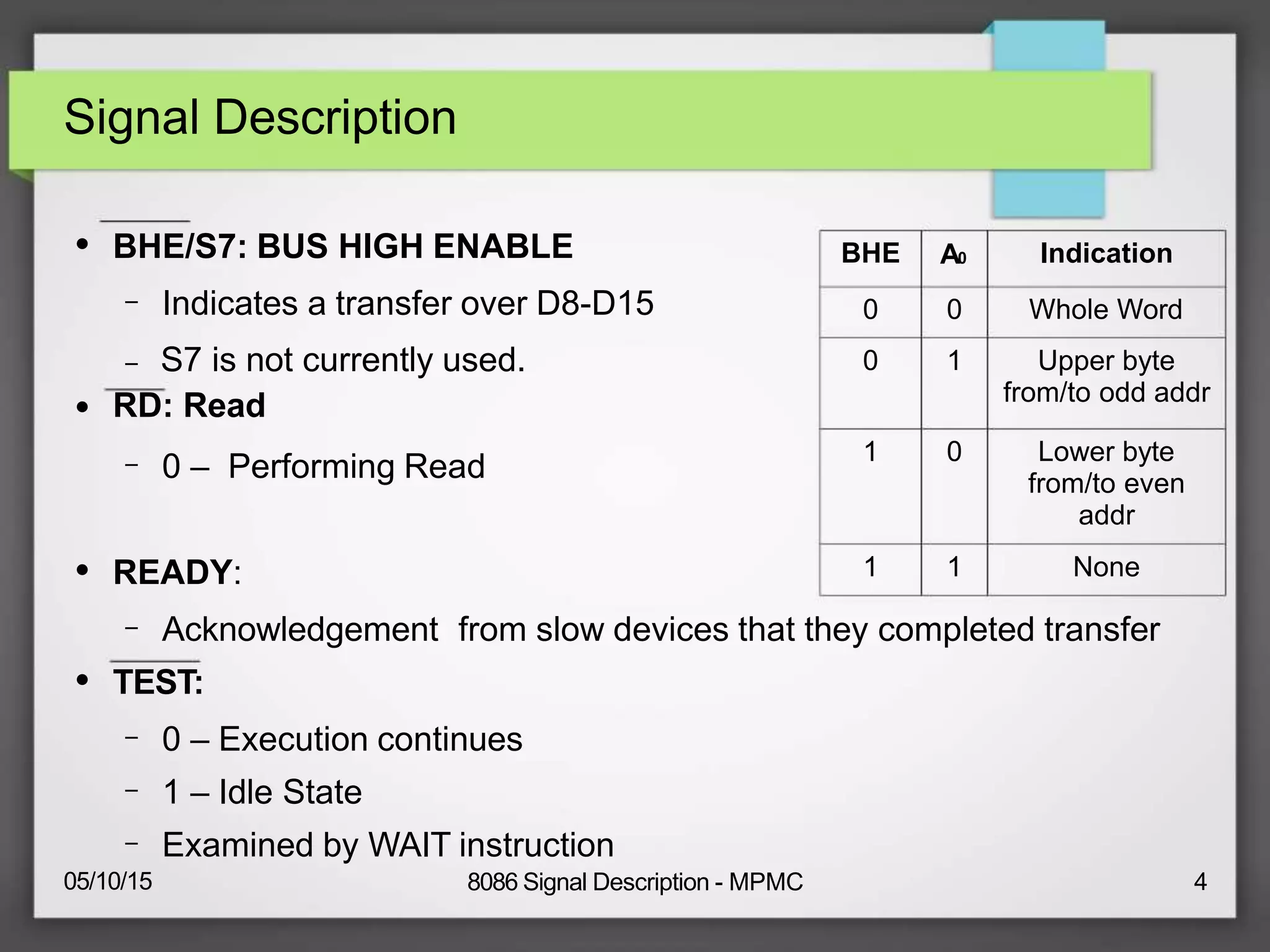
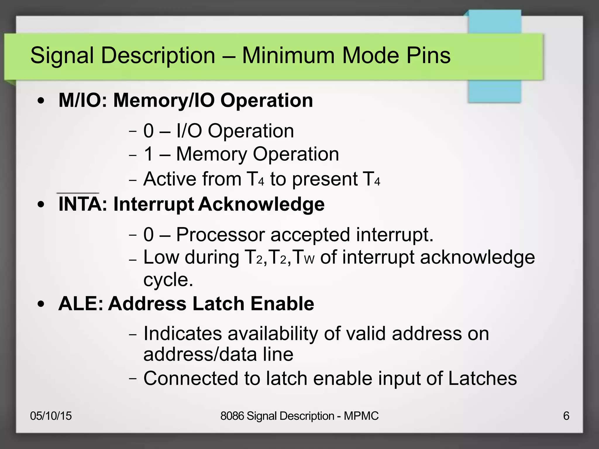
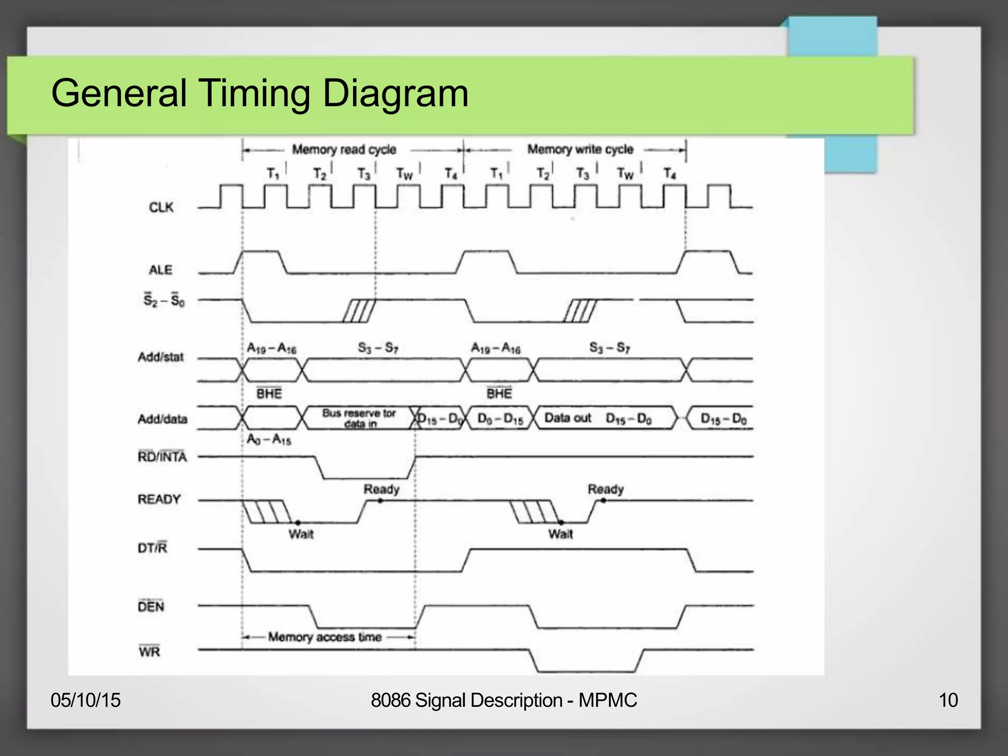
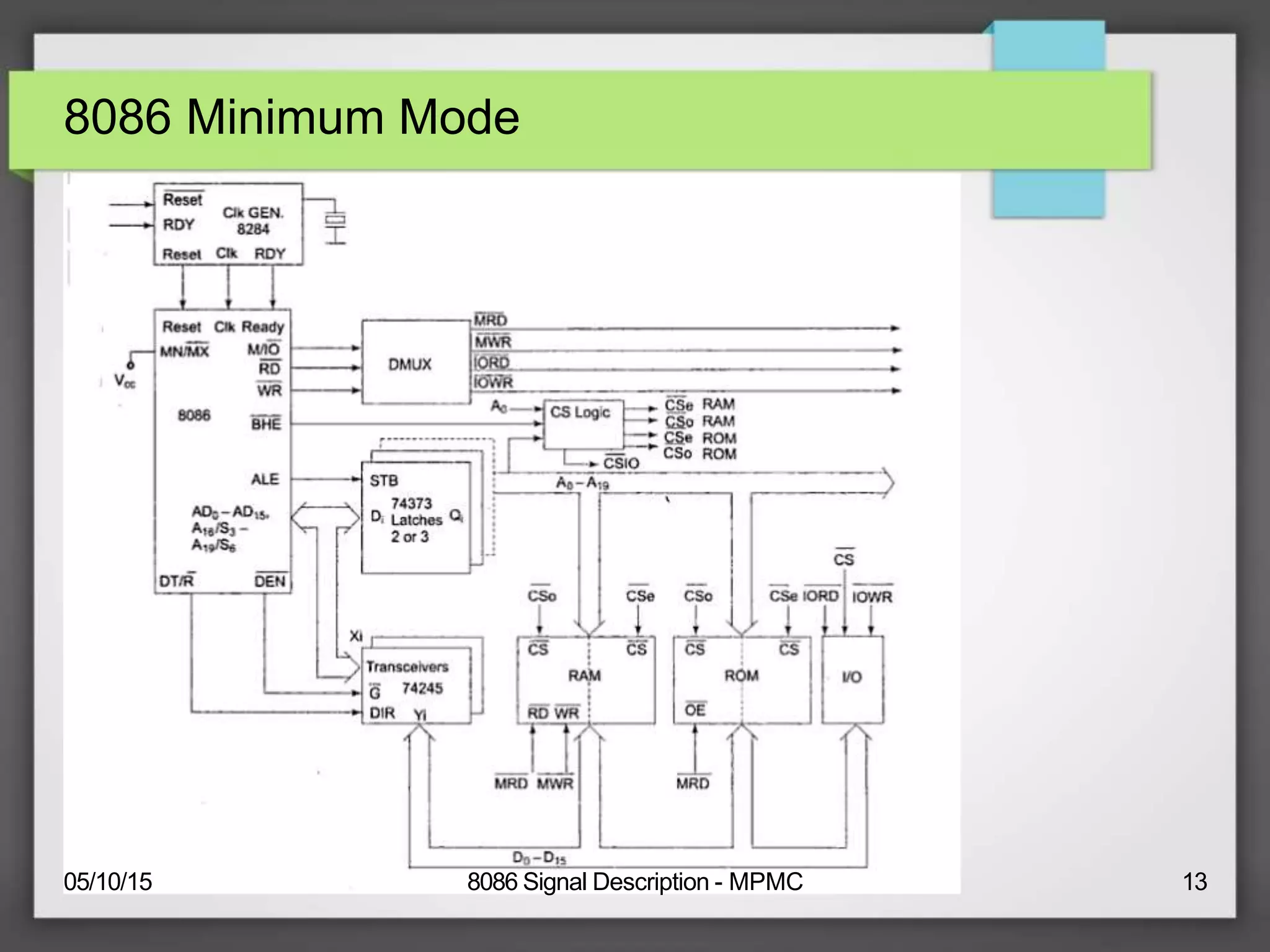
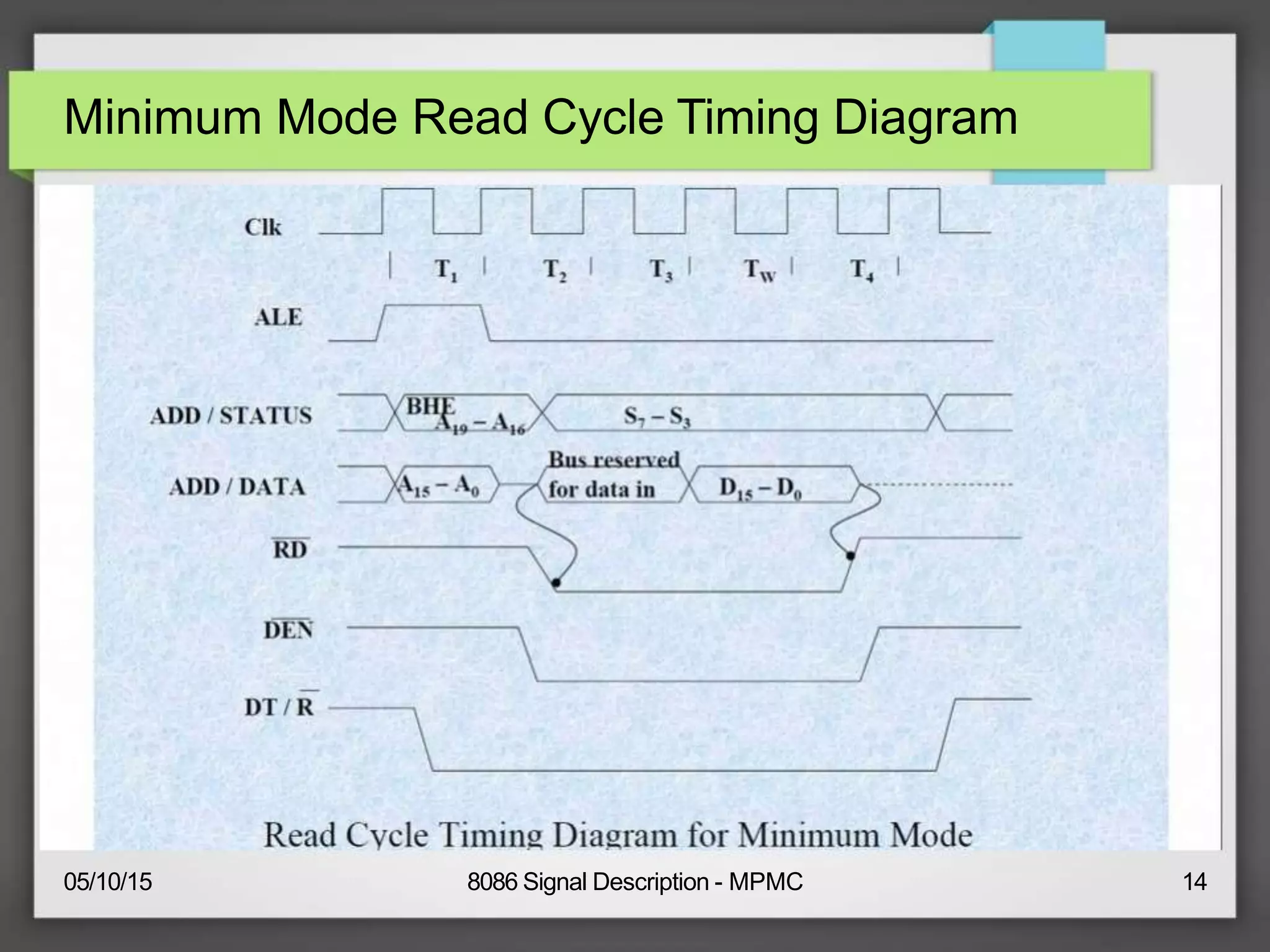
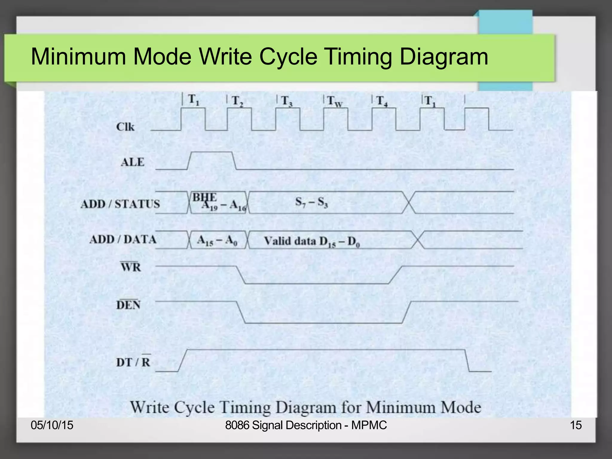
SlideShare a Scribd company logo
1 of 21
Microprocessors and Microcontrollers – 11EC311
Signal Description of 8086
Pin Diagram of 8086
05/10/15 8086 Signal Description - MPMC 2
Signal Description
AD15-AD0:
●
●
●
Time Multiplexed Address/Data Line
T1-Address Cycle
T2, T3, TW, T4- Data Cycle
● T are clock states of machine cycle
S4 S3 Indication
A19/S6- A16/S3: 0 0 Alternate Data
●
●
●
Time Multiplexed Address/Status Lines
During T1- Address line
During I/O these lines are low.
0 1
1 0
1 1
Stack
Code or None
Data
●
S5 -- status of IE Flag at beginning of each cycle.
●
S4 , S3 indicate segment register used for memory
●
●
Latches separate addr and status bits
S6 is always low
05/10/15 8086 Signal Description - MPMC 3
Signal Description
●
BHE/S7: BUS HIGH ENABLE BHE A0 Indication
– Indicates a transfer over D8-D15 0 0 Whole Word
●
– S7 is not currently used.
RD: Read
0 1 Upper byte
from/to odd addr
– 0 – Performing Read 1 0 Lower byte
from/to even
addr
●
READY: 1 1 None
– Acknowledgement from slow devices that they completed transfer
●
TEST:
–
–
–
05/10/15
0 – Execution continues
1 – Idle State
Examined by WAIT instruction
8086 Signal Description - MPMC 4
Signal Description
● INTR: Interrupt Request
–
–
Level triggered input
Sampled during last clock cycle of each instruction
to determine availability of request.
● NMI: Non-maskable interrupt
– Causes type 2 interrupt ( Cannot be Masked)
● RESET:
– Stops execution and starts from
FFFF0H● CLK: Clock Input
– Square wave of 33% duty Cycle. Range: 5Mhz- 10
MHz●
●
●
VCC: +5V
GND: Ground
MN/MX: 1-- Min Mode 0-- Max Mode
05/10/15 8086 Signal Description - MPMC 5
Signal Description – Minimum Mode Pins
● M/IO: Memory/IO Operation
–
–
–
0 – I/O Operation
1 – Memory Operation
Active from T4 to present T4
● INTA: Interrupt Acknowledge
–
–
0 – Processor accepted interrupt.
Low during T2,T2,TW of interrupt acknowledge
cycle.
● ALE: Address Latch Enable
–
–
Indicates availability of valid address on
address/data line
Connected to latch enable input of Latches
05/10/15 8086 Signal Description - MPMC 6
Signal Description – Minimum Mode Pins
● DT/R:Data Transmit or receive
–
–
–
1-Transmit
0- Receive
Same timing as M/IO
● DEN: Data Enable
–
–
–
Availability of valid data over address/data lines
Used to enable transreceivers to separate data from
multiplexed address/data signal.
Active from middle of T2 to middle of T4.
● HOLD/HLDA: Hold Acknowledge.
05/10/15
–
–
–
1 – Another master is requesting bus access
After hold processer gives hold acknowledge signal in
middle of next clock cycle after current instruction cycle.
0 – HDLA is also low
8086 Signal Description - MPMC 7
Signal Description – Maximum Mode Pins
●
●
S2,S1,S0:
– Status lines
– Active from T4 to current T1,T2
LOCK:
– 0 – Other system bus
masters will be prevented
from gaining system bus.
– Activated by LOCK prefix
Instruction..
S2
0
0
0
0
1
1
1
1
S1
0
0
1
1
0
0
1
1
S0
0
1
0
1
0
1
0
1
Indication
Interrupt
Acknowledge
Read I/O Port
Write I/O Port
Halt
Code access
Read memory
Write memory
Passive
05/10/15 8086 Signal Description - MPMC 8
Signal Description – Maximum Mode Pins
●
QS1, QS0 – Queue Status QS1 QS0 Indication
– Status of prefetch queue. 0 0 No Operation
●
RQ/GT0, RQ/GT1:
– Request/Grant
– Used by other local bus
0
1
1
1
0
1
First byte of opcode
from the queue
Empty Queue
Subsequent byte
from the queue
–
05/10/15
masters to force the processor to release the local bus at
end of processor’scurrent bus cycle.
RQ/GT0 have high priority than RQ/GT1.
8086 Signal Description - MPMC 9
General Timing Diagram
05/10/15 8086 Signal Description - MPMC 10
Possible Operations
●
●
●
●
Memory Read
Memory Write
IO Read
IO Write
05/10/15 8086 Signal Description - MPMC 11
Modes of Operation: Minimum Mode
●
●
Single Processor Mode
Latches are D-Flipflops( 74LS373/8282)
–
–
Demux address from addr/data signal
3 octal latches are required
● Transreceivers are bidirectional buffers(74245)
–
–
–
Demux data from addr/data signal
Controlled using DEN and DT/R 2
octal data buffers
● M/IO, RD , DEN indicate type of data transfer.
05/10/15 8086 Signal Description - MPMC 12
8086 Minimum Mode
05/10/15 8086 Signal Description - MPMC 13
Minimum Mode Read Cycle Timing Diagram
05/10/15 8086 Signal Description - MPMC 14
Minimum Mode Write Cycle Timing Diagram
05/10/15 8086 Signal Description - MPMC 15
Modes of Operation: Maximum Mode
●
●
●
●
●
●
Multi Processor Mode
Bus controller chip IC8288 derives outputs from given
signals.
ALE,DEN,DT/R,MRDC,MWTC,AMWC,IORC,IOWC,AIOWC
Memory Read Control, Memory Write Control
Advanced Memory Write Control
IO Read Control, IO Write Control
Advanced IO Write Control
05/10/15 8086 Signal Description - MPMC 16
8086 Maximum Mode
05/10/15 8086 Signal Description - MPMC 17
Maximum Mode Memory Read Timing Diagram
05/10/15 8086 Signal Description - MPMC 18
Maximum Mode Memory Write Timing Diagram
05/10/15 8086 Signal Description - MPMC 19
References
●
●
●
●
https://www.sites.google.com/site/sripathroykoganti/my-forms
D.V.Hall “Microprocessor and Interfacing”, 2nd Edition Tata McGraw
Hill Publishing Company,2006.
A.K. Ray & K. M Bhurchandi, “Advanced Microprocessors &
peripherals”, Tata Mc Graw Hill Publishing Company 2002.
Rajkamal, “Microcontrollers - Architecture, Programming, Interfacing
& System Design”, 2 nd edition, Pearson Education.
05/10/15 8086 Signal Description - MPMC 20
Thank You
05/10/15 8086 Signal Description - MPMC 21

More Related Content

What's hot

Minimum mode and Maximum mode Configuration in 8086
Minimum mode and Maximum mode Configuration in 8086Minimum mode and Maximum mode Configuration in 8086
Minimum mode and Maximum mode Configuration in 8086Jismy .K.Jose
 
Minimum And Maximum Modes Of 80826
Minimum And Maximum Modes Of 80826Minimum And Maximum Modes Of 80826
Minimum And Maximum Modes Of 80826LAVANYA PALANIYAPPAN
 
8086 in minimum mode
8086 in minimum mode8086 in minimum mode
8086 in minimum modeSridari Iyer
 
I/o and memory interfacing
I/o and memory interfacingI/o and memory interfacing
I/o and memory interfacingRuchi Srivastava
 
Pin configuration of 8085
Pin configuration of 8085Pin configuration of 8085
Pin configuration of 808582338476
 
Detailed Explanation of Pin Description of 8085 microprocessor
Detailed Explanation of Pin Description of  8085 microprocessorDetailed Explanation of Pin Description of  8085 microprocessor
Detailed Explanation of Pin Description of 8085 microprocessorRamesh Dabhole
 
Bus Structure, Memory and I/O Interfacing
Bus Structure, Memory and I/O InterfacingBus Structure, Memory and I/O Interfacing
Bus Structure, Memory and I/O InterfacingHetauda City College
 
Microprocessor & Interfacing (Part-1) By Er. Swapnil V. Kaware
Microprocessor & Interfacing (Part-1) By Er. Swapnil V. KawareMicroprocessor & Interfacing (Part-1) By Er. Swapnil V. Kaware
Microprocessor & Interfacing (Part-1) By Er. Swapnil V. KawareProf. Swapnil V. Kaware
 
Microprocessor & Interfacing (Part-2) By Er. Swapnil V. Kaware
Microprocessor & Interfacing (Part-2) By Er. Swapnil V. KawareMicroprocessor & Interfacing (Part-2) By Er. Swapnil V. Kaware
Microprocessor & Interfacing (Part-2) By Er. Swapnil V. KawareProf. Swapnil V. Kaware
 
8085 Interfacing with I/O Devices or Memory
8085 Interfacing with I/O Devices or Memory8085 Interfacing with I/O Devices or Memory
8085 Interfacing with I/O Devices or MemorySaumay Paul
 

What's hot (20)

Microprocessors 1-8086
Microprocessors 1-8086Microprocessors 1-8086
Microprocessors 1-8086
 
Microprocessors
MicroprocessorsMicroprocessors
Microprocessors
 
Minimum mode and Maximum mode Configuration in 8086
Minimum mode and Maximum mode Configuration in 8086Minimum mode and Maximum mode Configuration in 8086
Minimum mode and Maximum mode Configuration in 8086
 
Lect 5
Lect 5Lect 5
Lect 5
 
Minimum And Maximum Modes Of 80826
Minimum And Maximum Modes Of 80826Minimum And Maximum Modes Of 80826
Minimum And Maximum Modes Of 80826
 
8086 in minimum mode
8086 in minimum mode8086 in minimum mode
8086 in minimum mode
 
Chapter5
Chapter5Chapter5
Chapter5
 
I/o and memory interfacing
I/o and memory interfacingI/o and memory interfacing
I/o and memory interfacing
 
Pin configuration of 8085
Pin configuration of 8085Pin configuration of 8085
Pin configuration of 8085
 
Pin diagram 8085
Pin diagram 8085 Pin diagram 8085
Pin diagram 8085
 
Detailed Explanation of Pin Description of 8085 microprocessor
Detailed Explanation of Pin Description of  8085 microprocessorDetailed Explanation of Pin Description of  8085 microprocessor
Detailed Explanation of Pin Description of 8085 microprocessor
 
Bus Structure, Memory and I/O Interfacing
Bus Structure, Memory and I/O InterfacingBus Structure, Memory and I/O Interfacing
Bus Structure, Memory and I/O Interfacing
 
Microprocessor & Interfacing (Part-1) By Er. Swapnil V. Kaware
Microprocessor & Interfacing (Part-1) By Er. Swapnil V. KawareMicroprocessor & Interfacing (Part-1) By Er. Swapnil V. Kaware
Microprocessor & Interfacing (Part-1) By Er. Swapnil V. Kaware
 
Microprocessor & Interfacing (Part-2) By Er. Swapnil V. Kaware
Microprocessor & Interfacing (Part-2) By Er. Swapnil V. KawareMicroprocessor & Interfacing (Part-2) By Er. Swapnil V. Kaware
Microprocessor & Interfacing (Part-2) By Er. Swapnil V. Kaware
 
MINIMUM MODE INTERFACE
MINIMUM MODE INTERFACEMINIMUM MODE INTERFACE
MINIMUM MODE INTERFACE
 
8085 Interfacing with I/O Devices or Memory
8085 Interfacing with I/O Devices or Memory8085 Interfacing with I/O Devices or Memory
8085 Interfacing with I/O Devices or Memory
 
8086 microprocessor
8086 microprocessor8086 microprocessor
8086 microprocessor
 
Chapter 5
Chapter 5Chapter 5
Chapter 5
 
8085 microprocessor
8085 microprocessor8085 microprocessor
8085 microprocessor
 
8155 PPI
8155 PPI8155 PPI
8155 PPI
 

Similar to Coi2 pin description of 8086

3 L pin diagram.pptx
3 L pin diagram.pptx3 L pin diagram.pptx
3 L pin diagram.pptxPoonamarora73
 
Lecture 11 8086 Pin Diagram.pptx
Lecture 11 8086 Pin Diagram.pptxLecture 11 8086 Pin Diagram.pptx
Lecture 11 8086 Pin Diagram.pptxAbdullahbinzahir1
 
architecture of 8086 new Lecture 4new.pptx
architecture of 8086 new Lecture 4new.pptxarchitecture of 8086 new Lecture 4new.pptx
architecture of 8086 new Lecture 4new.pptxDrVikasMahor
 
Chapter 2_1(8086 System configuration).pptx
Chapter 2_1(8086 System configuration).pptxChapter 2_1(8086 System configuration).pptx
Chapter 2_1(8086 System configuration).pptxmelaku76
 
8086-microprocessor
8086-microprocessor8086-microprocessor
8086-microprocessorjhcid
 
8086 Microprocessor by Nitish Nagar
8086 Microprocessor by Nitish Nagar8086 Microprocessor by Nitish Nagar
8086 Microprocessor by Nitish NagarNitish Nagar
 
mic_unit1.pdf msbte unit 1 note pdf in ppt
mic_unit1.pdf msbte unit 1 note pdf in pptmic_unit1.pdf msbte unit 1 note pdf in ppt
mic_unit1.pdf msbte unit 1 note pdf in pptxboyxman1000
 
Microprocessors and Microcontrollers 8086 Pin Connections
Microprocessors and Microcontrollers 8086 Pin ConnectionsMicroprocessors and Microcontrollers 8086 Pin Connections
Microprocessors and Microcontrollers 8086 Pin ConnectionsJason J Pulikkottil
 
PPT on 8085 Microprocessor
PPT on 8085 Microprocessor  PPT on 8085 Microprocessor
PPT on 8085 Microprocessor DebrajJana4
 
8086 modes
8086 modes8086 modes
8086 modesPDFSHARE
 
EE8551 mpmc unit 1 module 5
EE8551 mpmc unit 1   module 5EE8551 mpmc unit 1   module 5
EE8551 mpmc unit 1 module 5CHAIRMA LAKSHMI
 
COA PRESENTATION 8085 machine cycle.pptx
COA PRESENTATION 8085 machine cycle.pptxCOA PRESENTATION 8085 machine cycle.pptx
COA PRESENTATION 8085 machine cycle.pptxAyush51240
 
UNIT 1 Microprocessors.pptx
UNIT 1 Microprocessors.pptxUNIT 1 Microprocessors.pptx
UNIT 1 Microprocessors.pptxGowrishankar C
 

Similar to Coi2 pin description of 8086 (20)

unit 4 mc.pdf
unit 4 mc.pdfunit 4 mc.pdf
unit 4 mc.pdf
 
8086 micro processor
8086 micro processor8086 micro processor
8086 micro processor
 
3 L pin diagram.pptx
3 L pin diagram.pptx3 L pin diagram.pptx
3 L pin diagram.pptx
 
Lecture 11 8086 Pin Diagram.pptx
Lecture 11 8086 Pin Diagram.pptxLecture 11 8086 Pin Diagram.pptx
Lecture 11 8086 Pin Diagram.pptx
 
architecture of 8086 new Lecture 4new.pptx
architecture of 8086 new Lecture 4new.pptxarchitecture of 8086 new Lecture 4new.pptx
architecture of 8086 new Lecture 4new.pptx
 
Chapter 2_1(8086 System configuration).pptx
Chapter 2_1(8086 System configuration).pptxChapter 2_1(8086 System configuration).pptx
Chapter 2_1(8086 System configuration).pptx
 
8086-microprocessor
8086-microprocessor8086-microprocessor
8086-microprocessor
 
pin-diagram of 8085_new.ppt
pin-diagram of 8085_new.pptpin-diagram of 8085_new.ppt
pin-diagram of 8085_new.ppt
 
timing diagram.pptx
timing diagram.pptxtiming diagram.pptx
timing diagram.pptx
 
8086 Microprocessor by Nitish Nagar
8086 Microprocessor by Nitish Nagar8086 Microprocessor by Nitish Nagar
8086 Microprocessor by Nitish Nagar
 
Microprocessor
MicroprocessorMicroprocessor
Microprocessor
 
mic_unit1.pdf msbte unit 1 note pdf in ppt
mic_unit1.pdf msbte unit 1 note pdf in pptmic_unit1.pdf msbte unit 1 note pdf in ppt
mic_unit1.pdf msbte unit 1 note pdf in ppt
 
Microprocessors and Microcontrollers 8086 Pin Connections
Microprocessors and Microcontrollers 8086 Pin ConnectionsMicroprocessors and Microcontrollers 8086 Pin Connections
Microprocessors and Microcontrollers 8086 Pin Connections
 
Pin description of 8086
Pin description of 8086Pin description of 8086
Pin description of 8086
 
PPT on 8085 Microprocessor
PPT on 8085 Microprocessor  PPT on 8085 Microprocessor
PPT on 8085 Microprocessor
 
8086 modes
8086 modes8086 modes
8086 modes
 
EE8551 mpmc unit 1 module 5
EE8551 mpmc unit 1   module 5EE8551 mpmc unit 1   module 5
EE8551 mpmc unit 1 module 5
 
8085.ppt
8085.ppt8085.ppt
8085.ppt
 
COA PRESENTATION 8085 machine cycle.pptx
COA PRESENTATION 8085 machine cycle.pptxCOA PRESENTATION 8085 machine cycle.pptx
COA PRESENTATION 8085 machine cycle.pptx
 
UNIT 1 Microprocessors.pptx
UNIT 1 Microprocessors.pptxUNIT 1 Microprocessors.pptx
UNIT 1 Microprocessors.pptx
 

Recently uploaded

9548086042 for call girls in Indira Nagar with room service
9548086042  for call girls in Indira Nagar  with room service9548086042  for call girls in Indira Nagar  with room service
9548086042 for call girls in Indira Nagar with room servicediscovermytutordmt
 
Accessible design: Minimum effort, maximum impact
Accessible design: Minimum effort, maximum impactAccessible design: Minimum effort, maximum impact
Accessible design: Minimum effort, maximum impactdawncurless
 
APM Welcome, APM North West Network Conference, Synergies Across Sectors
APM Welcome, APM North West Network Conference, Synergies Across SectorsAPM Welcome, APM North West Network Conference, Synergies Across Sectors
APM Welcome, APM North West Network Conference, Synergies Across SectorsAssociation for Project Management
 
The basics of sentences session 2pptx copy.pptx
The basics of sentences session 2pptx copy.pptxThe basics of sentences session 2pptx copy.pptx
The basics of sentences session 2pptx copy.pptxheathfieldcps1
 
BAG TECHNIQUE Bag technique-a tool making use of public health bag through wh...
BAG TECHNIQUE Bag technique-a tool making use of public health bag through wh...BAG TECHNIQUE Bag technique-a tool making use of public health bag through wh...
BAG TECHNIQUE Bag technique-a tool making use of public health bag through wh...Sapna Thakur
 
Arihant handbook biology for class 11 .pdf
Arihant handbook biology for class 11 .pdfArihant handbook biology for class 11 .pdf
Arihant handbook biology for class 11 .pdfchloefrazer622
 
Z Score,T Score, Percential Rank and Box Plot Graph
Z Score,T Score, Percential Rank and Box Plot GraphZ Score,T Score, Percential Rank and Box Plot Graph
Z Score,T Score, Percential Rank and Box Plot GraphThiyagu K
 
Presentation by Andreas Schleicher Tackling the School Absenteeism Crisis 30 ...
Presentation by Andreas Schleicher Tackling the School Absenteeism Crisis 30 ...Presentation by Andreas Schleicher Tackling the School Absenteeism Crisis 30 ...
Presentation by Andreas Schleicher Tackling the School Absenteeism Crisis 30 ...EduSkills OECD
 
Interactive Powerpoint_How to Master effective communication
Interactive Powerpoint_How to Master effective communicationInteractive Powerpoint_How to Master effective communication
Interactive Powerpoint_How to Master effective communicationnomboosow
 
The byproduct of sericulture in different industries.pptx
The byproduct of sericulture in different industries.pptxThe byproduct of sericulture in different industries.pptx
The byproduct of sericulture in different industries.pptxShobhayan Kirtania
 
Grant Readiness 101 TechSoup and Remy Consulting
Grant Readiness 101 TechSoup and Remy ConsultingGrant Readiness 101 TechSoup and Remy Consulting
Grant Readiness 101 TechSoup and Remy ConsultingTechSoup
 
A Critique of the Proposed National Education Policy Reform
A Critique of the Proposed National Education Policy ReformA Critique of the Proposed National Education Policy Reform
A Critique of the Proposed National Education Policy ReformChameera Dedduwage
 
Beyond the EU: DORA and NIS 2 Directive's Global Impact
Beyond the EU: DORA and NIS 2 Directive's Global ImpactBeyond the EU: DORA and NIS 2 Directive's Global Impact
Beyond the EU: DORA and NIS 2 Directive's Global ImpactPECB
 
The Most Excellent Way | 1 Corinthians 13
The Most Excellent Way | 1 Corinthians 13The Most Excellent Way | 1 Corinthians 13
The Most Excellent Way | 1 Corinthians 13Steve Thomason
 
Activity 01 - Artificial Culture (1).pdf
Activity 01 - Artificial Culture (1).pdfActivity 01 - Artificial Culture (1).pdf
Activity 01 - Artificial Culture (1).pdfciinovamais
 
POINT- BIOCHEMISTRY SEM 2 ENZYMES UNIT 5.pptx
POINT- BIOCHEMISTRY SEM 2 ENZYMES UNIT 5.pptxPOINT- BIOCHEMISTRY SEM 2 ENZYMES UNIT 5.pptx
POINT- BIOCHEMISTRY SEM 2 ENZYMES UNIT 5.pptxSayali Powar
 
Q4-W6-Restating Informational Text Grade 3
Q4-W6-Restating Informational Text Grade 3Q4-W6-Restating Informational Text Grade 3
Q4-W6-Restating Informational Text Grade 3JemimahLaneBuaron
 
Paris 2024 Olympic Geographies - an activity
Paris 2024 Olympic Geographies - an activityParis 2024 Olympic Geographies - an activity
Paris 2024 Olympic Geographies - an activityGeoBlogs
 
SOCIAL AND HISTORICAL CONTEXT - LFTVD.pptx
SOCIAL AND HISTORICAL CONTEXT - LFTVD.pptxSOCIAL AND HISTORICAL CONTEXT - LFTVD.pptx
SOCIAL AND HISTORICAL CONTEXT - LFTVD.pptxiammrhaywood
 
Call Girls in Dwarka Mor Delhi Contact Us 9654467111
Call Girls in Dwarka Mor Delhi Contact Us 9654467111Call Girls in Dwarka Mor Delhi Contact Us 9654467111
Call Girls in Dwarka Mor Delhi Contact Us 9654467111Sapana Sha
 

Recently uploaded (20)

9548086042 for call girls in Indira Nagar with room service
9548086042  for call girls in Indira Nagar  with room service9548086042  for call girls in Indira Nagar  with room service
9548086042 for call girls in Indira Nagar with room service
 
Accessible design: Minimum effort, maximum impact
Accessible design: Minimum effort, maximum impactAccessible design: Minimum effort, maximum impact
Accessible design: Minimum effort, maximum impact
 
APM Welcome, APM North West Network Conference, Synergies Across Sectors
APM Welcome, APM North West Network Conference, Synergies Across SectorsAPM Welcome, APM North West Network Conference, Synergies Across Sectors
APM Welcome, APM North West Network Conference, Synergies Across Sectors
 
The basics of sentences session 2pptx copy.pptx
The basics of sentences session 2pptx copy.pptxThe basics of sentences session 2pptx copy.pptx
The basics of sentences session 2pptx copy.pptx
 
BAG TECHNIQUE Bag technique-a tool making use of public health bag through wh...
BAG TECHNIQUE Bag technique-a tool making use of public health bag through wh...BAG TECHNIQUE Bag technique-a tool making use of public health bag through wh...
BAG TECHNIQUE Bag technique-a tool making use of public health bag through wh...
 
Arihant handbook biology for class 11 .pdf
Arihant handbook biology for class 11 .pdfArihant handbook biology for class 11 .pdf
Arihant handbook biology for class 11 .pdf
 
Z Score,T Score, Percential Rank and Box Plot Graph
Z Score,T Score, Percential Rank and Box Plot GraphZ Score,T Score, Percential Rank and Box Plot Graph
Z Score,T Score, Percential Rank and Box Plot Graph
 
Presentation by Andreas Schleicher Tackling the School Absenteeism Crisis 30 ...
Presentation by Andreas Schleicher Tackling the School Absenteeism Crisis 30 ...Presentation by Andreas Schleicher Tackling the School Absenteeism Crisis 30 ...
Presentation by Andreas Schleicher Tackling the School Absenteeism Crisis 30 ...
 
Interactive Powerpoint_How to Master effective communication
Interactive Powerpoint_How to Master effective communicationInteractive Powerpoint_How to Master effective communication
Interactive Powerpoint_How to Master effective communication
 
The byproduct of sericulture in different industries.pptx
The byproduct of sericulture in different industries.pptxThe byproduct of sericulture in different industries.pptx
The byproduct of sericulture in different industries.pptx
 
Grant Readiness 101 TechSoup and Remy Consulting
Grant Readiness 101 TechSoup and Remy ConsultingGrant Readiness 101 TechSoup and Remy Consulting
Grant Readiness 101 TechSoup and Remy Consulting
 
A Critique of the Proposed National Education Policy Reform
A Critique of the Proposed National Education Policy ReformA Critique of the Proposed National Education Policy Reform
A Critique of the Proposed National Education Policy Reform
 
Beyond the EU: DORA and NIS 2 Directive's Global Impact
Beyond the EU: DORA and NIS 2 Directive's Global ImpactBeyond the EU: DORA and NIS 2 Directive's Global Impact
Beyond the EU: DORA and NIS 2 Directive's Global Impact
 
The Most Excellent Way | 1 Corinthians 13
The Most Excellent Way | 1 Corinthians 13The Most Excellent Way | 1 Corinthians 13
The Most Excellent Way | 1 Corinthians 13
 
Activity 01 - Artificial Culture (1).pdf
Activity 01 - Artificial Culture (1).pdfActivity 01 - Artificial Culture (1).pdf
Activity 01 - Artificial Culture (1).pdf
 
POINT- BIOCHEMISTRY SEM 2 ENZYMES UNIT 5.pptx
POINT- BIOCHEMISTRY SEM 2 ENZYMES UNIT 5.pptxPOINT- BIOCHEMISTRY SEM 2 ENZYMES UNIT 5.pptx
POINT- BIOCHEMISTRY SEM 2 ENZYMES UNIT 5.pptx
 
Q4-W6-Restating Informational Text Grade 3
Q4-W6-Restating Informational Text Grade 3Q4-W6-Restating Informational Text Grade 3
Q4-W6-Restating Informational Text Grade 3
 
Paris 2024 Olympic Geographies - an activity
Paris 2024 Olympic Geographies - an activityParis 2024 Olympic Geographies - an activity
Paris 2024 Olympic Geographies - an activity
 
SOCIAL AND HISTORICAL CONTEXT - LFTVD.pptx
SOCIAL AND HISTORICAL CONTEXT - LFTVD.pptxSOCIAL AND HISTORICAL CONTEXT - LFTVD.pptx
SOCIAL AND HISTORICAL CONTEXT - LFTVD.pptx
 
Call Girls in Dwarka Mor Delhi Contact Us 9654467111
Call Girls in Dwarka Mor Delhi Contact Us 9654467111Call Girls in Dwarka Mor Delhi Contact Us 9654467111
Call Girls in Dwarka Mor Delhi Contact Us 9654467111
 

Coi2 pin description of 8086

  • 1. Microprocessors and Microcontrollers – 11EC311 Signal Description of 8086
  • 2. Pin Diagram of 8086 05/10/15 8086 Signal Description - MPMC 2
  • 3. Signal Description AD15-AD0: ● ● ● Time Multiplexed Address/Data Line T1-Address Cycle T2, T3, TW, T4- Data Cycle ● T are clock states of machine cycle S4 S3 Indication A19/S6- A16/S3: 0 0 Alternate Data ● ● ● Time Multiplexed Address/Status Lines During T1- Address line During I/O these lines are low. 0 1 1 0 1 1 Stack Code or None Data ● S5 -- status of IE Flag at beginning of each cycle. ● S4 , S3 indicate segment register used for memory ● ● Latches separate addr and status bits S6 is always low 05/10/15 8086 Signal Description - MPMC 3
  • 4. Signal Description ● BHE/S7: BUS HIGH ENABLE BHE A0 Indication – Indicates a transfer over D8-D15 0 0 Whole Word ● – S7 is not currently used. RD: Read 0 1 Upper byte from/to odd addr – 0 – Performing Read 1 0 Lower byte from/to even addr ● READY: 1 1 None – Acknowledgement from slow devices that they completed transfer ● TEST: – – – 05/10/15 0 – Execution continues 1 – Idle State Examined by WAIT instruction 8086 Signal Description - MPMC 4
  • 5. Signal Description ● INTR: Interrupt Request – – Level triggered input Sampled during last clock cycle of each instruction to determine availability of request. ● NMI: Non-maskable interrupt – Causes type 2 interrupt ( Cannot be Masked) ● RESET: – Stops execution and starts from FFFF0H● CLK: Clock Input – Square wave of 33% duty Cycle. Range: 5Mhz- 10 MHz● ● ● VCC: +5V GND: Ground MN/MX: 1-- Min Mode 0-- Max Mode 05/10/15 8086 Signal Description - MPMC 5
  • 6. Signal Description – Minimum Mode Pins ● M/IO: Memory/IO Operation – – – 0 – I/O Operation 1 – Memory Operation Active from T4 to present T4 ● INTA: Interrupt Acknowledge – – 0 – Processor accepted interrupt. Low during T2,T2,TW of interrupt acknowledge cycle. ● ALE: Address Latch Enable – – Indicates availability of valid address on address/data line Connected to latch enable input of Latches 05/10/15 8086 Signal Description - MPMC 6
  • 7. Signal Description – Minimum Mode Pins ● DT/R:Data Transmit or receive – – – 1-Transmit 0- Receive Same timing as M/IO ● DEN: Data Enable – – – Availability of valid data over address/data lines Used to enable transreceivers to separate data from multiplexed address/data signal. Active from middle of T2 to middle of T4. ● HOLD/HLDA: Hold Acknowledge. 05/10/15 – – – 1 – Another master is requesting bus access After hold processer gives hold acknowledge signal in middle of next clock cycle after current instruction cycle. 0 – HDLA is also low 8086 Signal Description - MPMC 7
  • 8. Signal Description – Maximum Mode Pins ● ● S2,S1,S0: – Status lines – Active from T4 to current T1,T2 LOCK: – 0 – Other system bus masters will be prevented from gaining system bus. – Activated by LOCK prefix Instruction.. S2 0 0 0 0 1 1 1 1 S1 0 0 1 1 0 0 1 1 S0 0 1 0 1 0 1 0 1 Indication Interrupt Acknowledge Read I/O Port Write I/O Port Halt Code access Read memory Write memory Passive 05/10/15 8086 Signal Description - MPMC 8
  • 9. Signal Description – Maximum Mode Pins ● QS1, QS0 – Queue Status QS1 QS0 Indication – Status of prefetch queue. 0 0 No Operation ● RQ/GT0, RQ/GT1: – Request/Grant – Used by other local bus 0 1 1 1 0 1 First byte of opcode from the queue Empty Queue Subsequent byte from the queue – 05/10/15 masters to force the processor to release the local bus at end of processor’scurrent bus cycle. RQ/GT0 have high priority than RQ/GT1. 8086 Signal Description - MPMC 9
  • 10. General Timing Diagram 05/10/15 8086 Signal Description - MPMC 10
  • 11. Possible Operations ● ● ● ● Memory Read Memory Write IO Read IO Write 05/10/15 8086 Signal Description - MPMC 11
  • 12. Modes of Operation: Minimum Mode ● ● Single Processor Mode Latches are D-Flipflops( 74LS373/8282) – – Demux address from addr/data signal 3 octal latches are required ● Transreceivers are bidirectional buffers(74245) – – – Demux data from addr/data signal Controlled using DEN and DT/R 2 octal data buffers ● M/IO, RD , DEN indicate type of data transfer. 05/10/15 8086 Signal Description - MPMC 12
  • 13. 8086 Minimum Mode 05/10/15 8086 Signal Description - MPMC 13
  • 14. Minimum Mode Read Cycle Timing Diagram 05/10/15 8086 Signal Description - MPMC 14
  • 15. Minimum Mode Write Cycle Timing Diagram 05/10/15 8086 Signal Description - MPMC 15
  • 16. Modes of Operation: Maximum Mode ● ● ● ● ● ● Multi Processor Mode Bus controller chip IC8288 derives outputs from given signals. ALE,DEN,DT/R,MRDC,MWTC,AMWC,IORC,IOWC,AIOWC Memory Read Control, Memory Write Control Advanced Memory Write Control IO Read Control, IO Write Control Advanced IO Write Control 05/10/15 8086 Signal Description - MPMC 16
  • 17. 8086 Maximum Mode 05/10/15 8086 Signal Description - MPMC 17
  • 18. Maximum Mode Memory Read Timing Diagram 05/10/15 8086 Signal Description - MPMC 18
  • 19. Maximum Mode Memory Write Timing Diagram 05/10/15 8086 Signal Description - MPMC 19
  • 20. References ● ● ● ● https://www.sites.google.com/site/sripathroykoganti/my-forms D.V.Hall “Microprocessor and Interfacing”, 2nd Edition Tata McGraw Hill Publishing Company,2006. A.K. Ray & K. M Bhurchandi, “Advanced Microprocessors & peripherals”, Tata Mc Graw Hill Publishing Company 2002. Rajkamal, “Microcontrollers - Architecture, Programming, Interfacing & System Design”, 2 nd edition, Pearson Education. 05/10/15 8086 Signal Description - MPMC 20
  • 21. Thank You 05/10/15 8086 Signal Description - MPMC 21