SlideShare a Scribd company logo
1 of 39
Download to read offline
INDEX
Draw the pin diagram of 8085 and explain the function of each pin 4
Differentiate Memory mapped IO and IO mapped IO 9
Show the memory interfacing of the following memory module with the 8085 with
proper circuit diagram neatly 8 KB EPROM (0000H-IFFFH)4KBRAM(8000H-8FFFH)
2KBEPROM (FO0OH-FTFFH) 10
Draw the block diagram of 8086 and describe the function of each unit in details 13
Write down the addressing modes of 8086 with at least two example of each.17
Define cache memory and virtual memory. 20
Differentiate protected virtual addressing mode and real addressing mode 20
Explain the control word format for 8255 in details 22
Show the interfacing of 8251 with processor with suitable diagram 25
Super scalar architecture 28
8279 Intel Keyboard Controller 30
Why crystal is a preferred clock source? 32
What is the Maximum clock frequency in 8086? 5 MHz to 10 MHz
Explain briefly register indirect addressing mode 32
What is cache memory? 34
Give two examples of 3 byte instruction? 35
What is meant by the term 'protected virtual address mode'? 38
Difference between cycle stealing DMA and transfer DMA? 39
What is the polling method in microprocessor 41
What is vectored interrupt 41
Briefly define the purpose of ready PIN in 8085 41
What is the use of ALE 42
What is the purpose of SOD and SID in 8085 42
What is wait state
What is a T-State
Draw and explain the timing diagram of memory read cycle of 8085
Explain direct addressing and indirect addressing mode in 8085 exmple
Program:
A) Load the number 5ch in register D
B) Load the number 9E H in register C
C) Increase the content of C by 1
D) Add the contents of C and D and output port 1
Explain the difference between JMP instruction and CALL instruction
Explain the memory mapped IO addressing scheme
What are hardware and software interrupts
What is ISS
How to transfer data using interrupts
What is asynchronous data transfer
Write the features of mode 0 in 8085
What is the use of 8251 chip
Define PPI
Explain the block diagram and define the function of each block of the 8251 USART
What are the features of the 8259 PIC
What is 8257 DMA Controller
How DMA operations are performed
Briefly state the function of mode set register in 8257
Discuss the function of instruction queue in 8086
Define pipelining
Describe the significance of LOCK signal in 8086
What is multi-user operating system? Describe any three addressing modes of 8086
with suitable examples. What is super scalar architecture?
What is the basic difference between 'protected virtual address mode' and 'real
address mode in microprocessor? What is memory management of an operating
system? What are the function of bus interface unit (BIU) in 8086
Why interfacing is needed for IO devices
What is Block transfer mode DMA?
How clock signal is generated in 8086? List the functions of Bus Interface unit in 8086.
What is the difference between segment register and general purpose register?
function of auxiliary carry flag used in 8086
Name the different addressing modes used in 8086 instruction set and explain about
one with suitable example
What is the operation performed when TEST input pin is low?
What is cache memory? What is the advantage of cache memory?
What is the difference between real mode and protected mode memory addressing?
What is dual pipeline architecture?
1. Address Bus and Data Bus:
The address bus is a group of sixteen lines i.e A0-A15. The address bus is
unidirectional, i.e., bits flow in one direction from the microprocessor unit to
the peripheral devices and uses the high order address bus.
2. Control and Status Signals:
• ALE – It is an Address Latch Enable signal. It goes high during first T state
of a machine cycle and enables the lower 8-bits of the address, if its value is
1 otherwise data bus is activated.
• IO/M’ – It is a status signal which determines whether the address is for
input-output or memory. When it is high(1) the address on the address bus
is for input-output devices. When it is low(0) the address on the address bus
is for the memory.
• SO, S1 – These are status signals. They distinguish the various types of
operations such as halt, reading, instruction fetching or writing.
• RD’ – It is a signal to control READ operation. When it is low the selected
memory or input-output device is read.
• WR’ – It is a signal to control WRITE operation. When it goes low the
data on the data bus is written into the selected memory or I/O location.
• READY – It senses whether a peripheral is ready to transfer data or not.
If READY is high(1) the peripheral is ready. If it is low(0) the microprocessor
waits till it goes high. It is useful for interfacing low speed devices.
3. Power Supply and Clock Frequency:
• Vcc – +5v power supply
• Vss – Ground Reference
• XI, X2 – A crystal is connected at these two pins. The frequency is
internally divided by two, therefore, to operate a system at 3MHZ the
crystal should have frequency of 6MHZ.
• CLK (OUT) – This signal can be used as the system clock for other
devices.
4. Interrupts and Peripheral Initiated Signals:
The 8085 has five interrupt signals that can be used to interrupt a program
execution.
(i) INTR
(ii) RST 7.5
(iii) RST 6.5
(iv) RST 5.5
(v) TRAP
The microprocessor acknowledges Interrupt Request by INTA’ signal. In addition
to Interrupts, there are three externally initiated signals namely RESET, HOLD
and READY. To respond to HOLD request, it has one signal called HLDA.
• INTR – It is an interrupt request signal.
• INTA’ – It is an interrupt acknowledgement sent by the microprocessor
after INTR is received.
5. Reset Signals:
• RESET IN’ – When the signal on this pin is low(0), the program-counter is
set to zero, the buses are tristated and the microprocessor unit is reset.
• RESET OUT – This signal indicates that the MPU is being reset. The signal
can be used to reset other devices.
6. DMA Signals:
• HOLD – It indicates that another device is requesting the use of the
address and data bus. Having received HOLD request the microprocessor
relinquishes the use of the buses as soon as the current machine cycle is
completed. Internal processing may continue. After the removal of the
HOLD signal the processor regains the bus.
• HLDA – It is a signal which indicates that the hold request has been
received after the removal of a HOLD request, the HLDA goes low.
7. Serial I/O Ports:
Serial transmission in 8085 is implemented by the two signals,
• SID and SOD – SID is a data line for serial input where as SOD is a data
line for serial output.
===============END======================
==============================END=============================
Interfacing memory chips with
8085
It is defined as the set of all possible addresses that a microprocessor can generate. 8085
microprocessor has a 16-bit address bus so that it can address 216 or 64 KB of address. It
called the address space of 8085. This total address space can be partitioned or allocated to
memory or I/O devices so that they can be addressed properly. This is called address space
partitioning.
We know 8085 has 16 address lines (A0 – A15). Hence a maximum of 64 KB (=
216 bytes) of memory locations can interfaced with 8085 microprocessor. The
memory address space of the 8085 takes values from 0000H to FFFFH. Hear H
denoted for Hexadecimal number.Another things we should know that the 8085
initiates set of signals such as IO/M, RD and WR when it wants to read from and
write into memory. Similarly, each memory chip has signals such as CE or CS (chip
enable or chip select), OE or RD (output enable or read) and WE or WR (write enable
or write) associated with it.
Now come to the main part when the 8085 wants to read from and write into
memory, it activates IO/M, RD and WR signals as shown in Table.
Table shows the status of IO/M, RD and WR signals during memory read and write
operations.
And interestingly microprocessor 8085 itself using IO/M, RD and WR signals, two
control signals MEMR (memory read) and MEMW (memory write) are generated. Fig.
1 shows the circuit used to generate these signals.
When is IO/M high, both memory control signals are deactivated irrespective of the
status Of RD and WR signals.
Now it will be very helpful to us if we discuss an example. For that we take an
example to elaborate the mater.
Ex: Interface an IC 2764 with 8085 using NAND gate address decoder such that the
address range allocate to the chip is 0000H – 1FFFH.
Specification of IC 2764:
• 8 KB (8 x 210 byte) EPROM chip
• 13 address lines (213 bytes = 8 KB)
Interfacing Process :
• 13 address lines of IC connected to the corresponding address lines of 8085.
• Remaining address lines of 8085 connected to address decoder formed using
logic gates, the output of which is connected to the CE pin of IC.
• Address range allocated to the chip shown in Table 9.
• Chip can enabled whenever the 8085 places an address allocated to EPROM
chip in the address bus.
===================================END==============================
=
8086 Microprocessor
Block Diagram of 8086 Microprocessor
The architecture of 8086 microprocessor is composed of 2 major units, the
BIU i.e., Bus Interface Unit and EU i.e., Execution Unit. The figure below
shows the block diagram of the architectural representation of the 8086
microprocessor:
Bus Interface Unit (BIU)
The Bus Interface Unit (BIU) manages the data, address and control buses.
The BIU functions in such a way that it:
• Fetches the sequenced instruction from the memory,
• Finds the physical address of that location in the memory where the
instruction is stored and
• Manages the 6-byte pre-fetch queue where the pipelined
instructions are stored.
An 8086 microprocessor exhibits the property of pipelining the instructions
in a queue while performing decoding and execution of the previous
instruction. This saves the processor time of operation by a large amount.
This pipelining is done in a 6-byte queue. Also, the BIU contains 4 segment
registers. Each segment register is 16-bit. The segments are present in the
memory and these registers hold the address of all the segments. These
registers are as follows:
1.Code segment register: It is a 16-bit register and holds the address of the
instruction or program stored in the code segment of the memory.
Also, the IP in the block diagram is the instruction pointer which is a default
register that is used by the processor in order to get the desired instruction.
The IP contains the offset address of the next byte that is to be taken from
the code segment.
2. Stack segment register: The stack segment register provides the starting
address of the stack segment in the memory. Like in stack pointer, PUSH
and POP operations are used in this segment to give and take the data
to/from it.
3. Data segment register: It holds the address of the data segment. The
data segment stores the data in the memory whose address is present in
this 16-bit register.
4. Extra segment register: Here the starting address of the extra segment is
present. This register basically contains the address of the string data.
It is to be noteworthy that the physical address of the instruction is
achieved by combining the segment address with that of the offset address.
6-byte pre-fetch queue: This queue is used in 8086 in order to perform
pipelining. As at the time of decoding and execution of the instruction in EU,
the BIU fetches the sequential upcoming instructions and stores it in this
queue.
The size of this queue is 6-byte. This means at maximum a 6-byte
instruction can be stored in this queue. The queue exhibits FIFO behavior.,
first in first out.
Execution Unit (EU)
The Execution Unit (EU) performs the decoding and execution of the
instructions that are being fetched from the desired memory location.
Control Unit:
Like the timing and control unit in 8085 microprocessor, the control unit in
8086 microprocessor produces control signal after decoding the opcode to
inform the general purpose register to release the value stored in it. And it
also signals the ALU to perform the desired operation.
ALU:
The arithmetic and logic unit carries out the logical tasks according to the
signal generated by the CU. The result of the operation is stored in the
desired register.
Flag:
Like in 8085, here also the flag register holds the status of the result
generated by the ALU. It has several flags that show the different
conditions of the result.
Operand:
It is a temporary register and is used by the processor to hold the
temporary values at the time of operation.
The reason behind two separate sections for BIU and EU in the architecture
of 8086 is to perform fetching and decoding-executing simultaneously.
===============================END==================================
=
Addressing modes in 8086
microprocessor
The way of specifying data to be operated by an instruction is known
as addressing modes. This specifies that the given data is an immediate data or
an address. It also specifies whether the given operand is register or register
pair.
Types of addressing modes:
1. Register mode – In this type of addressing mode both the operands are
registers.
Example:
MOV AX, BX
XOR AX, DX
ADD AL, BL
2.
3. Immediate mode – In this type of addressing mode the source operand
is a 8 bit or 16 bit data. Destination operand can never be immediate data.
Example:
MOV AX, 2000
MOV CL, 0A
ADD AL, 45
AND AX, 0000
4.
Note that to initialize the value of segment register an register is required.
MOV AX, 2000
MOV CS, AX
1. Displacement or direct mode – In this type of addressing mode the
effective address is directly given in the instruction as displacement.
Example:
MOV AX, [DISP]
MOV AX, [0500]
2.
3. Register indirect mode – In this addressing mode the effective address is
in SI, DI or BX.
Example:
MOV AX, [DI]
ADD AL, [BX]
MOV AX, [SI]
4.
5. Based indexed mode – In this the effective address is sum of base
register and index register.
Base register: BX, BP
Index register: SI, DI
6.
The physical memory address is calculated according to the base register.
Example:
7.
MOV AL, [BP+SI]
MOV AX, [BX+DI]
8.
9. Indexed mode – In this type of addressing mode the effective address is
sum of index register and displacement.
Example:
MOV AX, [SI+2000]
MOV AL, [DI+3000]
10.
11. Based mode – In this the effective address is the sum of base register
and displacement.
Example:
MOV AL, [BP+ 0100]
12.
13. Based indexed displacement mode – In this type of addressing mode the
effective address is the sum of index register, base register and
displacement.
Example:
MOV AL, [SI+BP+2000]
14.
15. String mode – This addressing mode is related to string instructions. In
this the value of SI and DI are auto incremented and decremented
depending upon the value of directional flag.
Example:
MOVS B
MOVS W
16.
17. Input/Output mode – This addressing mode is related with input output
operations.
Example:
IN A, 45
OUT A, 50
18.
19. Relative mode –
In this the effective address is calculated with reference to instruction
pointer.
Example:
JNZ 8 bit address
IP=IP+8 bit address
=========================END====================================
============================END============================
a port can be programmed to act as an input port or an output port. To tell about
that we generate a bit pattern or we may say a word which is called control word. A
control word is, therefore, to be formed for programming the ports of 8255A.The
format for the control word format for 8255A is shown in figure bellow. As per the
requirement of the programmer the control word is written into the control word
register of 8255A. No read operation of the control word is allowed.
So from above control word format for 8255A diagram we can see the bit wise
function of control word generation. Now we go for further description of the
control bits. We know in control word format it has 8 bits. In addition,every bit
responsible for respective work. Now see what are the work those bits do?
Bit D0 :
• Sets Port CLower as input or output port.
• To make Port CLower as input port this bit set to 1.
• To make Port CLower as output port this bit set to 0.
Bit D1:
• Sets Port B as input or output port.
• To make Port B as input port this bit set to 1.
• To make Port B as output port this bit set to 0.
Bit D2:
• This bit for mode selection for the port B.
• If this bit set to 0, the port B will operate in mode 0.
• If this bit set to 1, the port B will operate in mode 1.
Bit D3:
• Sets Port CUpper as input or output port.
• To make Port CUpper as input port this bit set to 1.
• To make Port CUpper as output port this bit set to 0.
Bit D4:
• Sets Port A as input or output port.
• To make Port A as input port this bit set to 1.
• To make Port A as output port this bit set to 0.
Bits D5 and D6 :
• These two bits mainly used for determining the I/O mode of port A.
Therefore, these bits are defined for the various modes of port A as follows.
Bit D7:
This bit specifies either I/O function or bit set/reset function (BSR mode). If this bit
set to 1 then the 8255 will work in I/O mode. If this bit set to 0 then the 8255 will
work in BSR mode.
There are 16 combinations of control words for various configurations of the ports of
8255 for Mode 0 operations. These control words are shown in table.
Finally it will be excellent enough if we are go through some Example.
Obtain the control word when the ports of 8255A are to be used in mode 0 with
port-A as output port and port B as input port and port C as output port.
Solution. The control word for this case shown in bellow.
===============================END====================================
The 8251 chip is Universal Synchronous Asynchronous Receiver Transmitter (USART).
It acts as a mediator between the microprocessor and peripheral devices. It converts
serial data to parallel form and vice versa. This chip is 28 pin DIP.
Now let us see the functional block diagram of the 8251 chip.
There are five different sections in this diagram. These sections are as follows
Read/ Write control logic
Transmitter
Receiver
Data Bus Buffer
Modem Control
Interfacing 8251 with8085
Now let us see how 8251 can be interfaced with 8085. In the diagram, we can see
that eight data lines D7-0 are connected to the data bus of the microprocessor. And
also the RD and WR of the 8251 are also connected with the RD and RD of 8051. The
8251 is getting the clock from the CLK OUT pin of 8085. And the RESET is also
connected to the RESET OUT pin of the microprocessor.
The C/D pin is used to select either control register or data register. This pin is
connected to the A0 pin of 8085. The CS pin of 8251 is attached to the output of an
address decoder circuit. The address decoder uses A7 to A1 lines of the
microprocessor. In this diagram the CS will be enabled when A7 and A4 is at logic 1,
and all other lines are at logic 0.
From the following table, we can see how to read or write data word, read the status
word and write control word.
=========================END=============================
Superscalar Architecture
A more aggressive approach is to equip the processor with multiple processing
units to handle several instructions in parallel in each processing stage. With
this arrangement, several instructions start execution in the same clock cycle
and the process is said to use multiple issue. Such processors are capable of
achieving an instruction execution throughput of more than one instruction per
cycle. They are known as ‘Superscalar Processors’.
In the above diagram, there is a processor with two execution units; one for
integer and one for floating point operations. The instruction fetch unit is
capable of reading the instructions at a time and storing them in the instruction
queue. In each cycle, the dispatch unit retrieves and decodes up to two
instructions from the front of the queue. If there is one integer, one floating
point instruction and no hazards, both the instructions are dispatched in the
same clock cycle.
Advantages of Superscalar Architecture :
• The compiler can avoid many hazards through judicious selection and
ordering of instructions.
• The compiler should strive to interleave floating point and integer
instructions. This would enable the dispatch unit to keep both the integer
and floating point units busy most of the time.
• In general, high performance is achieved if the compiler is able to
arrange program instructions to take maximum advantage of the available
hardware units.
Disadvantages of Superscalar Architecture :
• In a Superscalar Processor, the detrimental effect on performance of
various hazards becomes even more pronounced.
• Due to this type of architecture, problem in scheduling can occur.
=======================END=====================================
8279 programmable keyboard/display controller is designed by Intel that interfaces
a keyboard with the CPU. The keyboard first scans the keyboard and identifies if any
key has been pressed. It then sends their relative response of the pressed key to the
CPU and vice-a-versa.
How Does 8279 Keyboard Work?
The keyboard consists of maximum 64 keys, which are interfaced with the CPU by
using the key-codes. These key-codes are de-bounced and stored in an 8-byte
FIFORAM, which can be accessed by the CPU. If more than 8 characters are entered
in the FIFO, then it means more than eight keys are pressed at a time. This is when
the overrun status is set.
If a FIFO contains a valid key entry, then the CPU is interrupted in an interrupt mode
else the CPU checks the status in polling to read the entry. Once the CPU reads a
key entry, then FIFO is updated, and the key entry is pushed out of the FIFO to
generate space for new entries.
Architecture and Description
8279 − Pin Description
============================END=============================
Because of high stability, large Q (Quality Factor) & the frequency that doesn't drift
with aging
One need not have a crystal based oscillator for a microprocessor. Almost all
microprocessors give other options like RC,LC or external clock which are not accurate like a
crystal oscillator and could also be jittery. So, the question is why do we need an accurate
clock. It provides predictability of instruction execution time. For example with a 12MHZ
crystal, if an instruction takes 1 microsecond to execute, you can safely bet your program of
10 instructions will execute in 10 microseconds. Another important aspect could be counting
or timing you need to do with an intimidating accuracy. Now this accuracy comes because of
the quartz crytal you used.
===============END=========================
In this mode, the data is transferred from one register to another by using the
address pointed by the register. Register indirect addressing mode also used to call
as indirect addressing mode. For example MOV A, M: means data is transferred from
the memory address pointed by the register pair HLto the register A.
MOV E, M
It occupies only 1-Byte in memory. MOV E, M is an example instruction of this type.
It is a 1-Byte instruction. Suppose E register content is DBH, H register content is 40H,
and L register content is 50H. Letus say location 4050H has the data value AAH.
When the 8085 executes this instruction, the contents of E register will change to
AAH, as shown below –
The timing diagram for this MOV E, M instruction is as follows –
Summary: So this instruction MOV E, M requires1-Byte, 2-Machine Cycles (Opcode
Fetch, Memory Read) and 7 T-States for execution as shown in the timing diagram.
===========================END===============================
Cache Memory is a special very high-speed memory. It is used to speed up and
synchronizing with high-speed CPU. Cache memory is costlier than main
memory or disk memory but economical than CPU registers. Cache memory is
an extremely fast memory type that acts as a buffer between RAM and the CPU.
It holds frequently requested data and instructions so that they are
immediately available to the CPU when needed.
Cache memory is used to reduce the average time to access data from the Main
memory. The cache is a smaller and faster memory which stores copies of the
data from frequently used main memory locations. There are various different
independent caches in a CPU, which store instructions and data.
=========================END================================
3. Three-byte instructions –
Three-byte instruction is the type of instruction in which the first 8 bits
indicates the opcode and the next two bytes specify the 16-bit address. The
low-order address is represented in second byte and the high-order address is
represented in the third byte.
• Example-1:
Task- Load contents of memory 2050H in the accumulator.
Mnemonic- LDA 2050H
Opcode- LDA
Operand- 2050H
Hex Code- 3A
50
20
Binary code- 0011 1010
0101 0000
0010 0000
• Example-2:
Task- Transfer the program sequence to the memory location 2050H.
Mnemonic- JMP 2085H
Opcode- JMP
Operand- 2085H
Hex Code- C3
85
20
Binary code- 1100 0011
1000 0101
0010 0000
•
Note – These instructions would require three memory locations to store the
binary codes. The mnemonic is always followed by 16-bit (or adr).
================END=================
Protected Virtual Address Mode (PVAM)
80286 is the first processor to support the concepts of virtual memory and memory management.
The virtual memory does not exist physically it still appears to be available within the system.
Protected Virtual Address Mode (PVAM)
80286 is the first processor to support the concepts of virtual
memory and memory management. The virtual memory does not exist
physically it still appears to be available within the system. The concept
of VM is implemented using Physical memory that the CPU can directly
access and secondary memory that is used as a storage for data and
program, which are stored in secondary memory initially.
The Segment of the program or data required for actual execution
at that instant is fetched from the secondary memory into physical
memory. After the execution of this fetched segment, the next segment
required for further execution is again fetched from the secondary
memory, while the results of the executed segment are stored back into
the secondary memory for further references. This continues till the
complete program is executed
During the execution the partial results of the previously executed
portions are again fetched into the physical memory, if required for
further execution. The procedure of fetching the chosen program
segments or data from the secondary storage into physical memory is
called swapping. The procedure of storing back the partial results or
data back on the secondary storage is called unswapping. The virtual
memory is allotted per task.
The 80286 is able to address 1 G byte (230 bytes) of virtual
memory per task. The complete virtual memory is mapped on to the
16Mbyte physical memory. If a program larger than 16Mbyte is stored
on the hard disk and is to be executed, if it is fetched in terms of data or
program segments of less than 16Mbyte in size into the program
memory by swapping sequentially as per sequence of execution.
Whenever the portion of a program is required for execution by
the CPU, it is fetched from the secondary memory and placed in the
physical memory is called swapping in of the program. A portion of the
program or important partial results required for further execution, may
be saved back on secondary storage to make the PM free for further
execution of another required portion of the program is called swapping
out of the executable program.
80286 uses the 16-bit content of a segment register as a selector to
address a descriptor stored in the physical memory. The descriptor is a
block of contiguous memory locations containing information of a
segment, like segment base address, segment limit, segment type,
privilege level, segment availability in physical memory, descriptor type
and segment use another task.
===============================END==============================
==============================END================================
Polling:
In polling is not a hardware mechanism, its a protocol in which CPU steadily
checks whether the device needs attention. Wherever device tells process unit
that it desires hardware processing, in polling process unit keeps asking the I/O
device whether or not it desires CPU processing. The CPU ceaselessly check
every and each device hooked up thereto for sleuthing whether or not any
device desires hardware attention.
Each device features a command-ready bit that indicates the standing of that
device, i.e., whether or not it’s some command to be dead by hardware or not.
If command bit is ready one, then it’s some command to be dead else if the bit
is zero, then it’s no commands.
=================END===============================
In a computer, a vectored interrupt is an I/O interrupt that tells the part of
the computer that handles I/O interrupts at the hardware level that a
request for attention from an I/O device has been received and and also
identifies the device that sent the request.
A vectored interrupt is an alternative to a polled interrupt , which requires
that the interrupt handler poll or send a signal to each device in turn in
order to find out which one sent the interrupt request.
================END==============================
Ready: This is an active high input control signal. It is used by microprocessor to
detect whether a peripheral has completed (or is Ready for) the data transfer or not.
The main function of this pin is to synchronize slower peripheral to faster
microprocessor.
=================END=======================
Intel 8085 is an 8-bit microprocessor which has 16 address line for 16-bit address of
a memory location. 8 higher order address bits are transferred through 8 bit lines
out of this 16 address line while remaining lower order 8 bits of the address are sent
through another 8 lines multiplexed with the 8-bit data lines. ALE (Address Enable
Latch) is the control signal which is nothing but a positive going pulse generated
when a new operation is started by microprocessor. So when pulse goes high means
ALE=1, it makes address bus enable and when ALE=0, means low pulse makes data
bus enable.
Let us consider this following example and also the voltage level at ALE pin. If we
consider instruction MVI E, ABH then it means that ABH will be moved or copied to
the register E. And as a result the previous value of E will get over written.
=====================END=====================================
Serial I/O signals
There are 2 serial signals, i.e. SID and SOD and these signals are used for serial
communication.
SOD (Serial output data line) − The output SOD is set/reset as specified by
the SIM instruction.
SID (Serial input data line) − The data on this line is loaded into accumulator
whenever a RIM instruction is executed.
==============END========================

More Related Content

What's hot

8085 microprocessor Architecture and pin description
8085 microprocessor Architecture and pin description 8085 microprocessor Architecture and pin description
8085 microprocessor Architecture and pin description Vijay Kumar
 
PIN Specification of 8086 Microprocessor
PIN Specification of 8086 MicroprocessorPIN Specification of 8086 Microprocessor
PIN Specification of 8086 MicroprocessorNikhil Kumar
 
Basics of peripheral devices and Working
Basics of peripheral devices and WorkingBasics of peripheral devices and Working
Basics of peripheral devices and WorkingDr.YNM
 
Module 2 instruction set
Module 2 instruction set Module 2 instruction set
Module 2 instruction set Deepak John
 
Bus Structure, Memory and I/O Interfacing
Bus Structure, Memory and I/O InterfacingBus Structure, Memory and I/O Interfacing
Bus Structure, Memory and I/O InterfacingHetauda City College
 
Microprocessor & Interfacing (Part-1) By Er. Swapnil V. Kaware
Microprocessor & Interfacing (Part-1) By Er. Swapnil V. KawareMicroprocessor & Interfacing (Part-1) By Er. Swapnil V. Kaware
Microprocessor & Interfacing (Part-1) By Er. Swapnil V. KawareProf. Swapnil V. Kaware
 
Architecture OF 8085
Architecture OF 8085Architecture OF 8085
Architecture OF 8085muneer.k
 
architecture memory interfacing
architecture memory interfacingarchitecture memory interfacing
architecture memory interfacingShamsul Huda
 
MICROPROCESSOR 8085 WITH PROGRAMS
MICROPROCESSOR 8085 WITH PROGRAMSMICROPROCESSOR 8085 WITH PROGRAMS
MICROPROCESSOR 8085 WITH PROGRAMSSabin Gautam
 
Specialist officer it study material on organization of intel 8085 microproce...
Specialist officer it study material on organization of intel 8085 microproce...Specialist officer it study material on organization of intel 8085 microproce...
Specialist officer it study material on organization of intel 8085 microproce...Tamal Kumar Das
 
An introduction to microprocessor architecture using INTEL 8085 as a classic...
An introduction to microprocessor  architecture using INTEL 8085 as a classic...An introduction to microprocessor  architecture using INTEL 8085 as a classic...
An introduction to microprocessor architecture using INTEL 8085 as a classic...Prasad Deshpande
 
Microprocessor 8085 Chapter 3
Microprocessor 8085 Chapter 3Microprocessor 8085 Chapter 3
Microprocessor 8085 Chapter 3Rishikesh Bhavsar
 
Presentation on 8086 microprocessor
Presentation on 8086 microprocessorPresentation on 8086 microprocessor
Presentation on 8086 microprocessorDiponkor Bala
 
Pin Description and Register Organization of 8086 Microprocessor
Pin Description and Register Organization of 8086 MicroprocessorPin Description and Register Organization of 8086 Microprocessor
Pin Description and Register Organization of 8086 MicroprocessorMuthusamy Arumugam
 

What's hot (20)

8085 microprocessor Architecture and pin description
8085 microprocessor Architecture and pin description 8085 microprocessor Architecture and pin description
8085 microprocessor Architecture and pin description
 
Module 1 8086
Module 1 8086Module 1 8086
Module 1 8086
 
8085 microprocessor
8085 microprocessor8085 microprocessor
8085 microprocessor
 
PIN Specification of 8086 Microprocessor
PIN Specification of 8086 MicroprocessorPIN Specification of 8086 Microprocessor
PIN Specification of 8086 Microprocessor
 
microprocessor 8085
microprocessor 8085microprocessor 8085
microprocessor 8085
 
Basics of peripheral devices and Working
Basics of peripheral devices and WorkingBasics of peripheral devices and Working
Basics of peripheral devices and Working
 
Module 2 instruction set
Module 2 instruction set Module 2 instruction set
Module 2 instruction set
 
Bus Structure, Memory and I/O Interfacing
Bus Structure, Memory and I/O InterfacingBus Structure, Memory and I/O Interfacing
Bus Structure, Memory and I/O Interfacing
 
Microprocessor & Interfacing (Part-1) By Er. Swapnil V. Kaware
Microprocessor & Interfacing (Part-1) By Er. Swapnil V. KawareMicroprocessor & Interfacing (Part-1) By Er. Swapnil V. Kaware
Microprocessor & Interfacing (Part-1) By Er. Swapnil V. Kaware
 
Architecture OF 8085
Architecture OF 8085Architecture OF 8085
Architecture OF 8085
 
architecture memory interfacing
architecture memory interfacingarchitecture memory interfacing
architecture memory interfacing
 
MICROPROCESSOR 8085 WITH PROGRAMS
MICROPROCESSOR 8085 WITH PROGRAMSMICROPROCESSOR 8085 WITH PROGRAMS
MICROPROCESSOR 8085 WITH PROGRAMS
 
Specialist officer it study material on organization of intel 8085 microproce...
Specialist officer it study material on organization of intel 8085 microproce...Specialist officer it study material on organization of intel 8085 microproce...
Specialist officer it study material on organization of intel 8085 microproce...
 
An introduction to microprocessor architecture using INTEL 8085 as a classic...
An introduction to microprocessor  architecture using INTEL 8085 as a classic...An introduction to microprocessor  architecture using INTEL 8085 as a classic...
An introduction to microprocessor architecture using INTEL 8085 as a classic...
 
Microprocessor 8085 Chapter 3
Microprocessor 8085 Chapter 3Microprocessor 8085 Chapter 3
Microprocessor 8085 Chapter 3
 
Chapter 5
Chapter 5Chapter 5
Chapter 5
 
8085
80858085
8085
 
Presentation on 8086 microprocessor
Presentation on 8086 microprocessorPresentation on 8086 microprocessor
Presentation on 8086 microprocessor
 
Microprocessor
MicroprocessorMicroprocessor
Microprocessor
 
Pin Description and Register Organization of 8086 Microprocessor
Pin Description and Register Organization of 8086 MicroprocessorPin Description and Register Organization of 8086 Microprocessor
Pin Description and Register Organization of 8086 Microprocessor
 

Similar to Microprocessor questions converted

Ece 8085-microprocessor-ppt
Ece 8085-microprocessor-pptEce 8085-microprocessor-ppt
Ece 8085-microprocessor-pptsatyamshra
 
UNIT 1 Microprocessors.pptx
UNIT 1 Microprocessors.pptxUNIT 1 Microprocessors.pptx
UNIT 1 Microprocessors.pptxGowrishankar C
 
8085 microproceesor ppt
8085 microproceesor ppt8085 microproceesor ppt
8085 microproceesor pptRJ Aniket
 
MICROPROCESSOR AND INTERFACING
MICROPROCESSOR AND INTERFACING MICROPROCESSOR AND INTERFACING
MICROPROCESSOR AND INTERFACING Radhika Talaviya
 
MPMC UNIT-1. Microprocessor 8085 pdf Microprocessor and Microcontroller
MPMC UNIT-1. Microprocessor 8085 pdf Microprocessor and MicrocontrollerMPMC UNIT-1. Microprocessor 8085 pdf Microprocessor and Microcontroller
MPMC UNIT-1. Microprocessor 8085 pdf Microprocessor and MicrocontrollerRAHUL RANJAN
 
Microprocessor and Microcontroller.pdf
Microprocessor and Microcontroller.pdfMicroprocessor and Microcontroller.pdf
Microprocessor and Microcontroller.pdfLatif Khan
 
EEE- BEE603 - Microprocessor and Microcontroller- Mr K Dwarakesh_220819_18121...
EEE- BEE603 - Microprocessor and Microcontroller- Mr K Dwarakesh_220819_18121...EEE- BEE603 - Microprocessor and Microcontroller- Mr K Dwarakesh_220819_18121...
EEE- BEE603 - Microprocessor and Microcontroller- Mr K Dwarakesh_220819_18121...NaWinNK
 
T-states in microprocessor 8085
T-states in microprocessor 8085T-states in microprocessor 8085
T-states in microprocessor 8085yedles
 
Architecture and pin diagram of 8085
Architecture and pin diagram of 8085Architecture and pin diagram of 8085
Architecture and pin diagram of 8085Suchismita Paul
 
Micro Processor And Micro Controller for engineering in Pondicherry University
Micro Processor And Micro Controller for engineering in Pondicherry UniversityMicro Processor And Micro Controller for engineering in Pondicherry University
Micro Processor And Micro Controller for engineering in Pondicherry UniversityShyamShyam76
 

Similar to Microprocessor questions converted (20)

8085 microprocessor Embedded system
8085 microprocessor  Embedded system8085 microprocessor  Embedded system
8085 microprocessor Embedded system
 
8085.ppt
8085.ppt8085.ppt
8085.ppt
 
8085 intro
8085 intro8085 intro
8085 intro
 
8085 alp programs
8085 alp programs8085 alp programs
8085 alp programs
 
8085 (1)
8085 (1)8085 (1)
8085 (1)
 
Ece 8085-microprocessor-ppt
Ece 8085-microprocessor-pptEce 8085-microprocessor-ppt
Ece 8085-microprocessor-ppt
 
8085
80858085
8085
 
Eec503, mp 30 questions
Eec503, mp 30 questionsEec503, mp 30 questions
Eec503, mp 30 questions
 
Eec503, mp 30 questions
Eec503, mp 30 questionsEec503, mp 30 questions
Eec503, mp 30 questions
 
UNIT 1 Microprocessors.pptx
UNIT 1 Microprocessors.pptxUNIT 1 Microprocessors.pptx
UNIT 1 Microprocessors.pptx
 
Qb microprocessors
Qb microprocessorsQb microprocessors
Qb microprocessors
 
8085 microproceesor ppt
8085 microproceesor ppt8085 microproceesor ppt
8085 microproceesor ppt
 
MICROPROCESSOR AND INTERFACING
MICROPROCESSOR AND INTERFACING MICROPROCESSOR AND INTERFACING
MICROPROCESSOR AND INTERFACING
 
MPMC UNIT-1. Microprocessor 8085 pdf Microprocessor and Microcontroller
MPMC UNIT-1. Microprocessor 8085 pdf Microprocessor and MicrocontrollerMPMC UNIT-1. Microprocessor 8085 pdf Microprocessor and Microcontroller
MPMC UNIT-1. Microprocessor 8085 pdf Microprocessor and Microcontroller
 
EE6502 Microprocessor and Microcontroller
EE6502   Microprocessor and MicrocontrollerEE6502   Microprocessor and Microcontroller
EE6502 Microprocessor and Microcontroller
 
Microprocessor and Microcontroller.pdf
Microprocessor and Microcontroller.pdfMicroprocessor and Microcontroller.pdf
Microprocessor and Microcontroller.pdf
 
EEE- BEE603 - Microprocessor and Microcontroller- Mr K Dwarakesh_220819_18121...
EEE- BEE603 - Microprocessor and Microcontroller- Mr K Dwarakesh_220819_18121...EEE- BEE603 - Microprocessor and Microcontroller- Mr K Dwarakesh_220819_18121...
EEE- BEE603 - Microprocessor and Microcontroller- Mr K Dwarakesh_220819_18121...
 
T-states in microprocessor 8085
T-states in microprocessor 8085T-states in microprocessor 8085
T-states in microprocessor 8085
 
Architecture and pin diagram of 8085
Architecture and pin diagram of 8085Architecture and pin diagram of 8085
Architecture and pin diagram of 8085
 
Micro Processor And Micro Controller for engineering in Pondicherry University
Micro Processor And Micro Controller for engineering in Pondicherry UniversityMicro Processor And Micro Controller for engineering in Pondicherry University
Micro Processor And Micro Controller for engineering in Pondicherry University
 

More from ArghodeepPaul

Windows batch scripting
Windows batch scriptingWindows batch scripting
Windows batch scriptingArghodeepPaul
 
Common problems solving using c
Common problems solving using cCommon problems solving using c
Common problems solving using cArghodeepPaul
 
C variables and constants
C variables and constantsC variables and constants
C variables and constantsArghodeepPaul
 
Computer programming tools and building process
Computer programming tools and building processComputer programming tools and building process
Computer programming tools and building processArghodeepPaul
 
Algorithm pseudocode flowchart program notes
Algorithm pseudocode flowchart program notesAlgorithm pseudocode flowchart program notes
Algorithm pseudocode flowchart program notesArghodeepPaul
 
notes on Programming fundamentals
notes on Programming fundamentals notes on Programming fundamentals
notes on Programming fundamentals ArghodeepPaul
 

More from ArghodeepPaul (12)

Windows script host
Windows script hostWindows script host
Windows script host
 
Windows batch scripting
Windows batch scriptingWindows batch scripting
Windows batch scripting
 
Common problems solving using c
Common problems solving using cCommon problems solving using c
Common problems solving using c
 
C operators
C operatorsC operators
C operators
 
C taking user input
C taking user inputC taking user input
C taking user input
 
C storage classes
C storage classesC storage classes
C storage classes
 
C datatypes
C datatypesC datatypes
C datatypes
 
C variables and constants
C variables and constantsC variables and constants
C variables and constants
 
C program structure
C program structureC program structure
C program structure
 
Computer programming tools and building process
Computer programming tools and building processComputer programming tools and building process
Computer programming tools and building process
 
Algorithm pseudocode flowchart program notes
Algorithm pseudocode flowchart program notesAlgorithm pseudocode flowchart program notes
Algorithm pseudocode flowchart program notes
 
notes on Programming fundamentals
notes on Programming fundamentals notes on Programming fundamentals
notes on Programming fundamentals
 

Recently uploaded

High Profile Call Girls Nagpur Meera Call 7001035870 Meet With Nagpur Escorts
High Profile Call Girls Nagpur Meera Call 7001035870 Meet With Nagpur EscortsHigh Profile Call Girls Nagpur Meera Call 7001035870 Meet With Nagpur Escorts
High Profile Call Girls Nagpur Meera Call 7001035870 Meet With Nagpur EscortsCall Girls in Nagpur High Profile
 
Current Transformer Drawing and GTP for MSETCL
Current Transformer Drawing and GTP for MSETCLCurrent Transformer Drawing and GTP for MSETCL
Current Transformer Drawing and GTP for MSETCLDeelipZope
 
What are the advantages and disadvantages of membrane structures.pptx
What are the advantages and disadvantages of membrane structures.pptxWhat are the advantages and disadvantages of membrane structures.pptx
What are the advantages and disadvantages of membrane structures.pptxwendy cai
 
(MEERA) Dapodi Call Girls Just Call 7001035870 [ Cash on Delivery ] Pune Escorts
(MEERA) Dapodi Call Girls Just Call 7001035870 [ Cash on Delivery ] Pune Escorts(MEERA) Dapodi Call Girls Just Call 7001035870 [ Cash on Delivery ] Pune Escorts
(MEERA) Dapodi Call Girls Just Call 7001035870 [ Cash on Delivery ] Pune Escortsranjana rawat
 
Gurgaon ✡️9711147426✨Call In girls Gurgaon Sector 51 escort service
Gurgaon ✡️9711147426✨Call In girls Gurgaon Sector 51 escort serviceGurgaon ✡️9711147426✨Call In girls Gurgaon Sector 51 escort service
Gurgaon ✡️9711147426✨Call In girls Gurgaon Sector 51 escort servicejennyeacort
 
Gfe Mayur Vihar Call Girls Service WhatsApp -> 9999965857 Available 24x7 ^ De...
Gfe Mayur Vihar Call Girls Service WhatsApp -> 9999965857 Available 24x7 ^ De...Gfe Mayur Vihar Call Girls Service WhatsApp -> 9999965857 Available 24x7 ^ De...
Gfe Mayur Vihar Call Girls Service WhatsApp -> 9999965857 Available 24x7 ^ De...srsj9000
 
Oxy acetylene welding presentation note.
Oxy acetylene welding presentation note.Oxy acetylene welding presentation note.
Oxy acetylene welding presentation note.eptoze12
 
Introduction to Microprocesso programming and interfacing.pptx
Introduction to Microprocesso programming and interfacing.pptxIntroduction to Microprocesso programming and interfacing.pptx
Introduction to Microprocesso programming and interfacing.pptxvipinkmenon1
 
HARMONY IN THE NATURE AND EXISTENCE - Unit-IV
HARMONY IN THE NATURE AND EXISTENCE - Unit-IVHARMONY IN THE NATURE AND EXISTENCE - Unit-IV
HARMONY IN THE NATURE AND EXISTENCE - Unit-IVRajaP95
 
Heart Disease Prediction using machine learning.pptx
Heart Disease Prediction using machine learning.pptxHeart Disease Prediction using machine learning.pptx
Heart Disease Prediction using machine learning.pptxPoojaBan
 
College Call Girls Nashik Nehal 7001305949 Independent Escort Service Nashik
College Call Girls Nashik Nehal 7001305949 Independent Escort Service NashikCollege Call Girls Nashik Nehal 7001305949 Independent Escort Service Nashik
College Call Girls Nashik Nehal 7001305949 Independent Escort Service NashikCall Girls in Nagpur High Profile
 
Sheet Pile Wall Design and Construction: A Practical Guide for Civil Engineer...
Sheet Pile Wall Design and Construction: A Practical Guide for Civil Engineer...Sheet Pile Wall Design and Construction: A Practical Guide for Civil Engineer...
Sheet Pile Wall Design and Construction: A Practical Guide for Civil Engineer...Dr.Costas Sachpazis
 
VIP Call Girls Service Kondapur Hyderabad Call +91-8250192130
VIP Call Girls Service Kondapur Hyderabad Call +91-8250192130VIP Call Girls Service Kondapur Hyderabad Call +91-8250192130
VIP Call Girls Service Kondapur Hyderabad Call +91-8250192130Suhani Kapoor
 
OSVC_Meta-Data based Simulation Automation to overcome Verification Challenge...
OSVC_Meta-Data based Simulation Automation to overcome Verification Challenge...OSVC_Meta-Data based Simulation Automation to overcome Verification Challenge...
OSVC_Meta-Data based Simulation Automation to overcome Verification Challenge...Soham Mondal
 
Artificial-Intelligence-in-Electronics (K).pptx
Artificial-Intelligence-in-Electronics (K).pptxArtificial-Intelligence-in-Electronics (K).pptx
Artificial-Intelligence-in-Electronics (K).pptxbritheesh05
 
High Profile Call Girls Nagpur Isha Call 7001035870 Meet With Nagpur Escorts
High Profile Call Girls Nagpur Isha Call 7001035870 Meet With Nagpur EscortsHigh Profile Call Girls Nagpur Isha Call 7001035870 Meet With Nagpur Escorts
High Profile Call Girls Nagpur Isha Call 7001035870 Meet With Nagpur Escortsranjana rawat
 
VICTOR MAESTRE RAMIREZ - Planetary Defender on NASA's Double Asteroid Redirec...
VICTOR MAESTRE RAMIREZ - Planetary Defender on NASA's Double Asteroid Redirec...VICTOR MAESTRE RAMIREZ - Planetary Defender on NASA's Double Asteroid Redirec...
VICTOR MAESTRE RAMIREZ - Planetary Defender on NASA's Double Asteroid Redirec...VICTOR MAESTRE RAMIREZ
 
Biology for Computer Engineers Course Handout.pptx
Biology for Computer Engineers Course Handout.pptxBiology for Computer Engineers Course Handout.pptx
Biology for Computer Engineers Course Handout.pptxDeepakSakkari2
 

Recently uploaded (20)

High Profile Call Girls Nagpur Meera Call 7001035870 Meet With Nagpur Escorts
High Profile Call Girls Nagpur Meera Call 7001035870 Meet With Nagpur EscortsHigh Profile Call Girls Nagpur Meera Call 7001035870 Meet With Nagpur Escorts
High Profile Call Girls Nagpur Meera Call 7001035870 Meet With Nagpur Escorts
 
Current Transformer Drawing and GTP for MSETCL
Current Transformer Drawing and GTP for MSETCLCurrent Transformer Drawing and GTP for MSETCL
Current Transformer Drawing and GTP for MSETCL
 
What are the advantages and disadvantages of membrane structures.pptx
What are the advantages and disadvantages of membrane structures.pptxWhat are the advantages and disadvantages of membrane structures.pptx
What are the advantages and disadvantages of membrane structures.pptx
 
(MEERA) Dapodi Call Girls Just Call 7001035870 [ Cash on Delivery ] Pune Escorts
(MEERA) Dapodi Call Girls Just Call 7001035870 [ Cash on Delivery ] Pune Escorts(MEERA) Dapodi Call Girls Just Call 7001035870 [ Cash on Delivery ] Pune Escorts
(MEERA) Dapodi Call Girls Just Call 7001035870 [ Cash on Delivery ] Pune Escorts
 
Gurgaon ✡️9711147426✨Call In girls Gurgaon Sector 51 escort service
Gurgaon ✡️9711147426✨Call In girls Gurgaon Sector 51 escort serviceGurgaon ✡️9711147426✨Call In girls Gurgaon Sector 51 escort service
Gurgaon ✡️9711147426✨Call In girls Gurgaon Sector 51 escort service
 
Gfe Mayur Vihar Call Girls Service WhatsApp -> 9999965857 Available 24x7 ^ De...
Gfe Mayur Vihar Call Girls Service WhatsApp -> 9999965857 Available 24x7 ^ De...Gfe Mayur Vihar Call Girls Service WhatsApp -> 9999965857 Available 24x7 ^ De...
Gfe Mayur Vihar Call Girls Service WhatsApp -> 9999965857 Available 24x7 ^ De...
 
Oxy acetylene welding presentation note.
Oxy acetylene welding presentation note.Oxy acetylene welding presentation note.
Oxy acetylene welding presentation note.
 
Introduction to Microprocesso programming and interfacing.pptx
Introduction to Microprocesso programming and interfacing.pptxIntroduction to Microprocesso programming and interfacing.pptx
Introduction to Microprocesso programming and interfacing.pptx
 
HARMONY IN THE NATURE AND EXISTENCE - Unit-IV
HARMONY IN THE NATURE AND EXISTENCE - Unit-IVHARMONY IN THE NATURE AND EXISTENCE - Unit-IV
HARMONY IN THE NATURE AND EXISTENCE - Unit-IV
 
Heart Disease Prediction using machine learning.pptx
Heart Disease Prediction using machine learning.pptxHeart Disease Prediction using machine learning.pptx
Heart Disease Prediction using machine learning.pptx
 
College Call Girls Nashik Nehal 7001305949 Independent Escort Service Nashik
College Call Girls Nashik Nehal 7001305949 Independent Escort Service NashikCollege Call Girls Nashik Nehal 7001305949 Independent Escort Service Nashik
College Call Girls Nashik Nehal 7001305949 Independent Escort Service Nashik
 
Sheet Pile Wall Design and Construction: A Practical Guide for Civil Engineer...
Sheet Pile Wall Design and Construction: A Practical Guide for Civil Engineer...Sheet Pile Wall Design and Construction: A Practical Guide for Civil Engineer...
Sheet Pile Wall Design and Construction: A Practical Guide for Civil Engineer...
 
VIP Call Girls Service Kondapur Hyderabad Call +91-8250192130
VIP Call Girls Service Kondapur Hyderabad Call +91-8250192130VIP Call Girls Service Kondapur Hyderabad Call +91-8250192130
VIP Call Girls Service Kondapur Hyderabad Call +91-8250192130
 
OSVC_Meta-Data based Simulation Automation to overcome Verification Challenge...
OSVC_Meta-Data based Simulation Automation to overcome Verification Challenge...OSVC_Meta-Data based Simulation Automation to overcome Verification Challenge...
OSVC_Meta-Data based Simulation Automation to overcome Verification Challenge...
 
young call girls in Rajiv Chowk🔝 9953056974 🔝 Delhi escort Service
young call girls in Rajiv Chowk🔝 9953056974 🔝 Delhi escort Serviceyoung call girls in Rajiv Chowk🔝 9953056974 🔝 Delhi escort Service
young call girls in Rajiv Chowk🔝 9953056974 🔝 Delhi escort Service
 
Artificial-Intelligence-in-Electronics (K).pptx
Artificial-Intelligence-in-Electronics (K).pptxArtificial-Intelligence-in-Electronics (K).pptx
Artificial-Intelligence-in-Electronics (K).pptx
 
High Profile Call Girls Nagpur Isha Call 7001035870 Meet With Nagpur Escorts
High Profile Call Girls Nagpur Isha Call 7001035870 Meet With Nagpur EscortsHigh Profile Call Girls Nagpur Isha Call 7001035870 Meet With Nagpur Escorts
High Profile Call Girls Nagpur Isha Call 7001035870 Meet With Nagpur Escorts
 
VICTOR MAESTRE RAMIREZ - Planetary Defender on NASA's Double Asteroid Redirec...
VICTOR MAESTRE RAMIREZ - Planetary Defender on NASA's Double Asteroid Redirec...VICTOR MAESTRE RAMIREZ - Planetary Defender on NASA's Double Asteroid Redirec...
VICTOR MAESTRE RAMIREZ - Planetary Defender on NASA's Double Asteroid Redirec...
 
Biology for Computer Engineers Course Handout.pptx
Biology for Computer Engineers Course Handout.pptxBiology for Computer Engineers Course Handout.pptx
Biology for Computer Engineers Course Handout.pptx
 
🔝9953056974🔝!!-YOUNG call girls in Rajendra Nagar Escort rvice Shot 2000 nigh...
🔝9953056974🔝!!-YOUNG call girls in Rajendra Nagar Escort rvice Shot 2000 nigh...🔝9953056974🔝!!-YOUNG call girls in Rajendra Nagar Escort rvice Shot 2000 nigh...
🔝9953056974🔝!!-YOUNG call girls in Rajendra Nagar Escort rvice Shot 2000 nigh...
 

Microprocessor questions converted

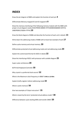
  • 1. INDEX Draw the pin diagram of 8085 and explain the function of each pin 4 Differentiate Memory mapped IO and IO mapped IO 9 Show the memory interfacing of the following memory module with the 8085 with proper circuit diagram neatly 8 KB EPROM (0000H-IFFFH)4KBRAM(8000H-8FFFH) 2KBEPROM (FO0OH-FTFFH) 10 Draw the block diagram of 8086 and describe the function of each unit in details 13 Write down the addressing modes of 8086 with at least two example of each.17 Define cache memory and virtual memory. 20 Differentiate protected virtual addressing mode and real addressing mode 20 Explain the control word format for 8255 in details 22 Show the interfacing of 8251 with processor with suitable diagram 25 Super scalar architecture 28 8279 Intel Keyboard Controller 30 Why crystal is a preferred clock source? 32 What is the Maximum clock frequency in 8086? 5 MHz to 10 MHz Explain briefly register indirect addressing mode 32 What is cache memory? 34 Give two examples of 3 byte instruction? 35 What is meant by the term 'protected virtual address mode'? 38 Difference between cycle stealing DMA and transfer DMA? 39
  • 2. What is the polling method in microprocessor 41 What is vectored interrupt 41 Briefly define the purpose of ready PIN in 8085 41 What is the use of ALE 42 What is the purpose of SOD and SID in 8085 42 What is wait state What is a T-State Draw and explain the timing diagram of memory read cycle of 8085 Explain direct addressing and indirect addressing mode in 8085 exmple Program: A) Load the number 5ch in register D B) Load the number 9E H in register C C) Increase the content of C by 1 D) Add the contents of C and D and output port 1 Explain the difference between JMP instruction and CALL instruction Explain the memory mapped IO addressing scheme What are hardware and software interrupts What is ISS How to transfer data using interrupts What is asynchronous data transfer Write the features of mode 0 in 8085 What is the use of 8251 chip Define PPI Explain the block diagram and define the function of each block of the 8251 USART What are the features of the 8259 PIC
  • 3. What is 8257 DMA Controller How DMA operations are performed Briefly state the function of mode set register in 8257 Discuss the function of instruction queue in 8086 Define pipelining Describe the significance of LOCK signal in 8086 What is multi-user operating system? Describe any three addressing modes of 8086 with suitable examples. What is super scalar architecture? What is the basic difference between 'protected virtual address mode' and 'real address mode in microprocessor? What is memory management of an operating system? What are the function of bus interface unit (BIU) in 8086 Why interfacing is needed for IO devices What is Block transfer mode DMA? How clock signal is generated in 8086? List the functions of Bus Interface unit in 8086. What is the difference between segment register and general purpose register? function of auxiliary carry flag used in 8086 Name the different addressing modes used in 8086 instruction set and explain about one with suitable example What is the operation performed when TEST input pin is low? What is cache memory? What is the advantage of cache memory? What is the difference between real mode and protected mode memory addressing? What is dual pipeline architecture?
  • 4. 1. Address Bus and Data Bus: The address bus is a group of sixteen lines i.e A0-A15. The address bus is
  • 5. unidirectional, i.e., bits flow in one direction from the microprocessor unit to the peripheral devices and uses the high order address bus. 2. Control and Status Signals: • ALE – It is an Address Latch Enable signal. It goes high during first T state of a machine cycle and enables the lower 8-bits of the address, if its value is 1 otherwise data bus is activated. • IO/M’ – It is a status signal which determines whether the address is for input-output or memory. When it is high(1) the address on the address bus is for input-output devices. When it is low(0) the address on the address bus is for the memory. • SO, S1 – These are status signals. They distinguish the various types of operations such as halt, reading, instruction fetching or writing.
  • 6. • RD’ – It is a signal to control READ operation. When it is low the selected memory or input-output device is read. • WR’ – It is a signal to control WRITE operation. When it goes low the data on the data bus is written into the selected memory or I/O location. • READY – It senses whether a peripheral is ready to transfer data or not. If READY is high(1) the peripheral is ready. If it is low(0) the microprocessor waits till it goes high. It is useful for interfacing low speed devices. 3. Power Supply and Clock Frequency: • Vcc – +5v power supply • Vss – Ground Reference • XI, X2 – A crystal is connected at these two pins. The frequency is internally divided by two, therefore, to operate a system at 3MHZ the crystal should have frequency of 6MHZ. • CLK (OUT) – This signal can be used as the system clock for other devices. 4. Interrupts and Peripheral Initiated Signals: The 8085 has five interrupt signals that can be used to interrupt a program execution. (i) INTR (ii) RST 7.5 (iii) RST 6.5 (iv) RST 5.5 (v) TRAP The microprocessor acknowledges Interrupt Request by INTA’ signal. In addition to Interrupts, there are three externally initiated signals namely RESET, HOLD and READY. To respond to HOLD request, it has one signal called HLDA. • INTR – It is an interrupt request signal. • INTA’ – It is an interrupt acknowledgement sent by the microprocessor after INTR is received.
  • 7. 5. Reset Signals: • RESET IN’ – When the signal on this pin is low(0), the program-counter is set to zero, the buses are tristated and the microprocessor unit is reset. • RESET OUT – This signal indicates that the MPU is being reset. The signal can be used to reset other devices. 6. DMA Signals: • HOLD – It indicates that another device is requesting the use of the address and data bus. Having received HOLD request the microprocessor relinquishes the use of the buses as soon as the current machine cycle is completed. Internal processing may continue. After the removal of the HOLD signal the processor regains the bus. • HLDA – It is a signal which indicates that the hold request has been received after the removal of a HOLD request, the HLDA goes low. 7. Serial I/O Ports: Serial transmission in 8085 is implemented by the two signals, • SID and SOD – SID is a data line for serial input where as SOD is a data line for serial output. ===============END======================
  • 9. Interfacing memory chips with 8085 It is defined as the set of all possible addresses that a microprocessor can generate. 8085 microprocessor has a 16-bit address bus so that it can address 216 or 64 KB of address. It called the address space of 8085. This total address space can be partitioned or allocated to memory or I/O devices so that they can be addressed properly. This is called address space partitioning. We know 8085 has 16 address lines (A0 – A15). Hence a maximum of 64 KB (= 216 bytes) of memory locations can interfaced with 8085 microprocessor. The memory address space of the 8085 takes values from 0000H to FFFFH. Hear H denoted for Hexadecimal number.Another things we should know that the 8085 initiates set of signals such as IO/M, RD and WR when it wants to read from and write into memory. Similarly, each memory chip has signals such as CE or CS (chip enable or chip select), OE or RD (output enable or read) and WE or WR (write enable or write) associated with it. Now come to the main part when the 8085 wants to read from and write into memory, it activates IO/M, RD and WR signals as shown in Table. Table shows the status of IO/M, RD and WR signals during memory read and write operations. And interestingly microprocessor 8085 itself using IO/M, RD and WR signals, two control signals MEMR (memory read) and MEMW (memory write) are generated. Fig. 1 shows the circuit used to generate these signals.
  • 10. When is IO/M high, both memory control signals are deactivated irrespective of the status Of RD and WR signals. Now it will be very helpful to us if we discuss an example. For that we take an example to elaborate the mater. Ex: Interface an IC 2764 with 8085 using NAND gate address decoder such that the address range allocate to the chip is 0000H – 1FFFH. Specification of IC 2764: • 8 KB (8 x 210 byte) EPROM chip • 13 address lines (213 bytes = 8 KB) Interfacing Process : • 13 address lines of IC connected to the corresponding address lines of 8085. • Remaining address lines of 8085 connected to address decoder formed using logic gates, the output of which is connected to the CE pin of IC. • Address range allocated to the chip shown in Table 9. • Chip can enabled whenever the 8085 places an address allocated to EPROM chip in the address bus.
  • 12. 8086 Microprocessor Block Diagram of 8086 Microprocessor The architecture of 8086 microprocessor is composed of 2 major units, the BIU i.e., Bus Interface Unit and EU i.e., Execution Unit. The figure below shows the block diagram of the architectural representation of the 8086 microprocessor: Bus Interface Unit (BIU) The Bus Interface Unit (BIU) manages the data, address and control buses. The BIU functions in such a way that it: • Fetches the sequenced instruction from the memory,
  • 13. • Finds the physical address of that location in the memory where the instruction is stored and • Manages the 6-byte pre-fetch queue where the pipelined instructions are stored. An 8086 microprocessor exhibits the property of pipelining the instructions in a queue while performing decoding and execution of the previous instruction. This saves the processor time of operation by a large amount. This pipelining is done in a 6-byte queue. Also, the BIU contains 4 segment registers. Each segment register is 16-bit. The segments are present in the memory and these registers hold the address of all the segments. These registers are as follows: 1.Code segment register: It is a 16-bit register and holds the address of the instruction or program stored in the code segment of the memory. Also, the IP in the block diagram is the instruction pointer which is a default register that is used by the processor in order to get the desired instruction. The IP contains the offset address of the next byte that is to be taken from the code segment. 2. Stack segment register: The stack segment register provides the starting address of the stack segment in the memory. Like in stack pointer, PUSH and POP operations are used in this segment to give and take the data to/from it. 3. Data segment register: It holds the address of the data segment. The data segment stores the data in the memory whose address is present in this 16-bit register. 4. Extra segment register: Here the starting address of the extra segment is present. This register basically contains the address of the string data. It is to be noteworthy that the physical address of the instruction is achieved by combining the segment address with that of the offset address. 6-byte pre-fetch queue: This queue is used in 8086 in order to perform pipelining. As at the time of decoding and execution of the instruction in EU, the BIU fetches the sequential upcoming instructions and stores it in this queue.
  • 14. The size of this queue is 6-byte. This means at maximum a 6-byte instruction can be stored in this queue. The queue exhibits FIFO behavior., first in first out. Execution Unit (EU) The Execution Unit (EU) performs the decoding and execution of the instructions that are being fetched from the desired memory location. Control Unit: Like the timing and control unit in 8085 microprocessor, the control unit in 8086 microprocessor produces control signal after decoding the opcode to inform the general purpose register to release the value stored in it. And it also signals the ALU to perform the desired operation. ALU: The arithmetic and logic unit carries out the logical tasks according to the signal generated by the CU. The result of the operation is stored in the desired register. Flag: Like in 8085, here also the flag register holds the status of the result generated by the ALU. It has several flags that show the different conditions of the result. Operand: It is a temporary register and is used by the processor to hold the temporary values at the time of operation. The reason behind two separate sections for BIU and EU in the architecture of 8086 is to perform fetching and decoding-executing simultaneously. ===============================END================================== =
  • 15. Addressing modes in 8086 microprocessor The way of specifying data to be operated by an instruction is known as addressing modes. This specifies that the given data is an immediate data or an address. It also specifies whether the given operand is register or register pair. Types of addressing modes: 1. Register mode – In this type of addressing mode both the operands are registers. Example: MOV AX, BX XOR AX, DX ADD AL, BL 2. 3. Immediate mode – In this type of addressing mode the source operand is a 8 bit or 16 bit data. Destination operand can never be immediate data. Example: MOV AX, 2000 MOV CL, 0A ADD AL, 45 AND AX, 0000 4. Note that to initialize the value of segment register an register is required. MOV AX, 2000 MOV CS, AX
  • 16. 1. Displacement or direct mode – In this type of addressing mode the effective address is directly given in the instruction as displacement. Example: MOV AX, [DISP] MOV AX, [0500] 2. 3. Register indirect mode – In this addressing mode the effective address is in SI, DI or BX. Example: MOV AX, [DI] ADD AL, [BX] MOV AX, [SI] 4. 5. Based indexed mode – In this the effective address is sum of base register and index register. Base register: BX, BP Index register: SI, DI 6. The physical memory address is calculated according to the base register. Example: 7. MOV AL, [BP+SI] MOV AX, [BX+DI] 8. 9. Indexed mode – In this type of addressing mode the effective address is sum of index register and displacement. Example: MOV AX, [SI+2000] MOV AL, [DI+3000] 10. 11. Based mode – In this the effective address is the sum of base register and displacement. Example: MOV AL, [BP+ 0100] 12. 13. Based indexed displacement mode – In this type of addressing mode the effective address is the sum of index register, base register and
  • 17. displacement. Example: MOV AL, [SI+BP+2000] 14. 15. String mode – This addressing mode is related to string instructions. In this the value of SI and DI are auto incremented and decremented depending upon the value of directional flag. Example: MOVS B MOVS W 16. 17. Input/Output mode – This addressing mode is related with input output operations. Example: IN A, 45 OUT A, 50 18. 19. Relative mode – In this the effective address is calculated with reference to instruction pointer. Example: JNZ 8 bit address IP=IP+8 bit address =========================END====================================
  • 19. a port can be programmed to act as an input port or an output port. To tell about that we generate a bit pattern or we may say a word which is called control word. A control word is, therefore, to be formed for programming the ports of 8255A.The format for the control word format for 8255A is shown in figure bellow. As per the requirement of the programmer the control word is written into the control word register of 8255A. No read operation of the control word is allowed.
  • 20. So from above control word format for 8255A diagram we can see the bit wise function of control word generation. Now we go for further description of the control bits. We know in control word format it has 8 bits. In addition,every bit responsible for respective work. Now see what are the work those bits do? Bit D0 : • Sets Port CLower as input or output port. • To make Port CLower as input port this bit set to 1. • To make Port CLower as output port this bit set to 0. Bit D1: • Sets Port B as input or output port. • To make Port B as input port this bit set to 1. • To make Port B as output port this bit set to 0. Bit D2: • This bit for mode selection for the port B. • If this bit set to 0, the port B will operate in mode 0. • If this bit set to 1, the port B will operate in mode 1. Bit D3: • Sets Port CUpper as input or output port. • To make Port CUpper as input port this bit set to 1.
  • 21. • To make Port CUpper as output port this bit set to 0. Bit D4: • Sets Port A as input or output port. • To make Port A as input port this bit set to 1. • To make Port A as output port this bit set to 0. Bits D5 and D6 : • These two bits mainly used for determining the I/O mode of port A. Therefore, these bits are defined for the various modes of port A as follows. Bit D7: This bit specifies either I/O function or bit set/reset function (BSR mode). If this bit set to 1 then the 8255 will work in I/O mode. If this bit set to 0 then the 8255 will work in BSR mode. There are 16 combinations of control words for various configurations of the ports of 8255 for Mode 0 operations. These control words are shown in table.
  • 22. Finally it will be excellent enough if we are go through some Example. Obtain the control word when the ports of 8255A are to be used in mode 0 with port-A as output port and port B as input port and port C as output port. Solution. The control word for this case shown in bellow.
  • 23. ===============================END==================================== The 8251 chip is Universal Synchronous Asynchronous Receiver Transmitter (USART). It acts as a mediator between the microprocessor and peripheral devices. It converts serial data to parallel form and vice versa. This chip is 28 pin DIP.
  • 24. Now let us see the functional block diagram of the 8251 chip. There are five different sections in this diagram. These sections are as follows Read/ Write control logic Transmitter Receiver Data Bus Buffer Modem Control Interfacing 8251 with8085
  • 25. Now let us see how 8251 can be interfaced with 8085. In the diagram, we can see that eight data lines D7-0 are connected to the data bus of the microprocessor. And also the RD and WR of the 8251 are also connected with the RD and RD of 8051. The 8251 is getting the clock from the CLK OUT pin of 8085. And the RESET is also connected to the RESET OUT pin of the microprocessor. The C/D pin is used to select either control register or data register. This pin is connected to the A0 pin of 8085. The CS pin of 8251 is attached to the output of an address decoder circuit. The address decoder uses A7 to A1 lines of the microprocessor. In this diagram the CS will be enabled when A7 and A4 is at logic 1, and all other lines are at logic 0. From the following table, we can see how to read or write data word, read the status word and write control word.
  • 26. =========================END============================= Superscalar Architecture A more aggressive approach is to equip the processor with multiple processing units to handle several instructions in parallel in each processing stage. With this arrangement, several instructions start execution in the same clock cycle and the process is said to use multiple issue. Such processors are capable of achieving an instruction execution throughput of more than one instruction per cycle. They are known as ‘Superscalar Processors’.
  • 27. In the above diagram, there is a processor with two execution units; one for integer and one for floating point operations. The instruction fetch unit is capable of reading the instructions at a time and storing them in the instruction queue. In each cycle, the dispatch unit retrieves and decodes up to two instructions from the front of the queue. If there is one integer, one floating point instruction and no hazards, both the instructions are dispatched in the same clock cycle. Advantages of Superscalar Architecture : • The compiler can avoid many hazards through judicious selection and ordering of instructions. • The compiler should strive to interleave floating point and integer instructions. This would enable the dispatch unit to keep both the integer and floating point units busy most of the time. • In general, high performance is achieved if the compiler is able to arrange program instructions to take maximum advantage of the available hardware units. Disadvantages of Superscalar Architecture : • In a Superscalar Processor, the detrimental effect on performance of various hazards becomes even more pronounced.
  • 28. • Due to this type of architecture, problem in scheduling can occur. =======================END===================================== 8279 programmable keyboard/display controller is designed by Intel that interfaces a keyboard with the CPU. The keyboard first scans the keyboard and identifies if any key has been pressed. It then sends their relative response of the pressed key to the CPU and vice-a-versa. How Does 8279 Keyboard Work? The keyboard consists of maximum 64 keys, which are interfaced with the CPU by using the key-codes. These key-codes are de-bounced and stored in an 8-byte FIFORAM, which can be accessed by the CPU. If more than 8 characters are entered in the FIFO, then it means more than eight keys are pressed at a time. This is when the overrun status is set. If a FIFO contains a valid key entry, then the CPU is interrupted in an interrupt mode else the CPU checks the status in polling to read the entry. Once the CPU reads a key entry, then FIFO is updated, and the key entry is pushed out of the FIFO to generate space for new entries. Architecture and Description
  • 29.
  • 30. 8279 − Pin Description ============================END============================= Because of high stability, large Q (Quality Factor) & the frequency that doesn't drift with aging One need not have a crystal based oscillator for a microprocessor. Almost all microprocessors give other options like RC,LC or external clock which are not accurate like a crystal oscillator and could also be jittery. So, the question is why do we need an accurate clock. It provides predictability of instruction execution time. For example with a 12MHZ crystal, if an instruction takes 1 microsecond to execute, you can safely bet your program of 10 instructions will execute in 10 microseconds. Another important aspect could be counting or timing you need to do with an intimidating accuracy. Now this accuracy comes because of the quartz crytal you used.
  • 31. ===============END========================= In this mode, the data is transferred from one register to another by using the address pointed by the register. Register indirect addressing mode also used to call as indirect addressing mode. For example MOV A, M: means data is transferred from the memory address pointed by the register pair HLto the register A. MOV E, M It occupies only 1-Byte in memory. MOV E, M is an example instruction of this type. It is a 1-Byte instruction. Suppose E register content is DBH, H register content is 40H, and L register content is 50H. Letus say location 4050H has the data value AAH. When the 8085 executes this instruction, the contents of E register will change to AAH, as shown below – The timing diagram for this MOV E, M instruction is as follows –
  • 32. Summary: So this instruction MOV E, M requires1-Byte, 2-Machine Cycles (Opcode Fetch, Memory Read) and 7 T-States for execution as shown in the timing diagram. ===========================END=============================== Cache Memory is a special very high-speed memory. It is used to speed up and synchronizing with high-speed CPU. Cache memory is costlier than main memory or disk memory but economical than CPU registers. Cache memory is an extremely fast memory type that acts as a buffer between RAM and the CPU. It holds frequently requested data and instructions so that they are immediately available to the CPU when needed. Cache memory is used to reduce the average time to access data from the Main memory. The cache is a smaller and faster memory which stores copies of the data from frequently used main memory locations. There are various different independent caches in a CPU, which store instructions and data.
  • 33. =========================END================================ 3. Three-byte instructions – Three-byte instruction is the type of instruction in which the first 8 bits indicates the opcode and the next two bytes specify the 16-bit address. The low-order address is represented in second byte and the high-order address is represented in the third byte. • Example-1: Task- Load contents of memory 2050H in the accumulator. Mnemonic- LDA 2050H Opcode- LDA Operand- 2050H Hex Code- 3A 50 20 Binary code- 0011 1010 0101 0000 0010 0000 • Example-2: Task- Transfer the program sequence to the memory location 2050H. Mnemonic- JMP 2085H Opcode- JMP Operand- 2085H
  • 34. Hex Code- C3 85 20 Binary code- 1100 0011 1000 0101 0010 0000 • Note – These instructions would require three memory locations to store the binary codes. The mnemonic is always followed by 16-bit (or adr). ================END================= Protected Virtual Address Mode (PVAM) 80286 is the first processor to support the concepts of virtual memory and memory management. The virtual memory does not exist physically it still appears to be available within the system. Protected Virtual Address Mode (PVAM) 80286 is the first processor to support the concepts of virtual memory and memory management. The virtual memory does not exist physically it still appears to be available within the system. The concept of VM is implemented using Physical memory that the CPU can directly access and secondary memory that is used as a storage for data and program, which are stored in secondary memory initially.
  • 35. The Segment of the program or data required for actual execution at that instant is fetched from the secondary memory into physical memory. After the execution of this fetched segment, the next segment required for further execution is again fetched from the secondary memory, while the results of the executed segment are stored back into the secondary memory for further references. This continues till the complete program is executed During the execution the partial results of the previously executed portions are again fetched into the physical memory, if required for further execution. The procedure of fetching the chosen program segments or data from the secondary storage into physical memory is called swapping. The procedure of storing back the partial results or data back on the secondary storage is called unswapping. The virtual memory is allotted per task. The 80286 is able to address 1 G byte (230 bytes) of virtual memory per task. The complete virtual memory is mapped on to the 16Mbyte physical memory. If a program larger than 16Mbyte is stored on the hard disk and is to be executed, if it is fetched in terms of data or program segments of less than 16Mbyte in size into the program memory by swapping sequentially as per sequence of execution. Whenever the portion of a program is required for execution by the CPU, it is fetched from the secondary memory and placed in the physical memory is called swapping in of the program. A portion of the program or important partial results required for further execution, may be saved back on secondary storage to make the PM free for further execution of another required portion of the program is called swapping out of the executable program. 80286 uses the 16-bit content of a segment register as a selector to address a descriptor stored in the physical memory. The descriptor is a block of contiguous memory locations containing information of a segment, like segment base address, segment limit, segment type, privilege level, segment availability in physical memory, descriptor type and segment use another task.
  • 37. ==============================END================================ Polling: In polling is not a hardware mechanism, its a protocol in which CPU steadily checks whether the device needs attention. Wherever device tells process unit that it desires hardware processing, in polling process unit keeps asking the I/O device whether or not it desires CPU processing. The CPU ceaselessly check every and each device hooked up thereto for sleuthing whether or not any device desires hardware attention. Each device features a command-ready bit that indicates the standing of that device, i.e., whether or not it’s some command to be dead by hardware or not. If command bit is ready one, then it’s some command to be dead else if the bit is zero, then it’s no commands. =================END===============================
  • 38. In a computer, a vectored interrupt is an I/O interrupt that tells the part of the computer that handles I/O interrupts at the hardware level that a request for attention from an I/O device has been received and and also identifies the device that sent the request. A vectored interrupt is an alternative to a polled interrupt , which requires that the interrupt handler poll or send a signal to each device in turn in order to find out which one sent the interrupt request. ================END============================== Ready: This is an active high input control signal. It is used by microprocessor to detect whether a peripheral has completed (or is Ready for) the data transfer or not. The main function of this pin is to synchronize slower peripheral to faster microprocessor. =================END======================= Intel 8085 is an 8-bit microprocessor which has 16 address line for 16-bit address of a memory location. 8 higher order address bits are transferred through 8 bit lines out of this 16 address line while remaining lower order 8 bits of the address are sent through another 8 lines multiplexed with the 8-bit data lines. ALE (Address Enable Latch) is the control signal which is nothing but a positive going pulse generated when a new operation is started by microprocessor. So when pulse goes high means ALE=1, it makes address bus enable and when ALE=0, means low pulse makes data bus enable. Let us consider this following example and also the voltage level at ALE pin. If we consider instruction MVI E, ABH then it means that ABH will be moved or copied to the register E. And as a result the previous value of E will get over written.
  • 39. =====================END===================================== Serial I/O signals There are 2 serial signals, i.e. SID and SOD and these signals are used for serial communication. SOD (Serial output data line) − The output SOD is set/reset as specified by the SIM instruction. SID (Serial input data line) − The data on this line is loaded into accumulator whenever a RIM instruction is executed. ==============END========================