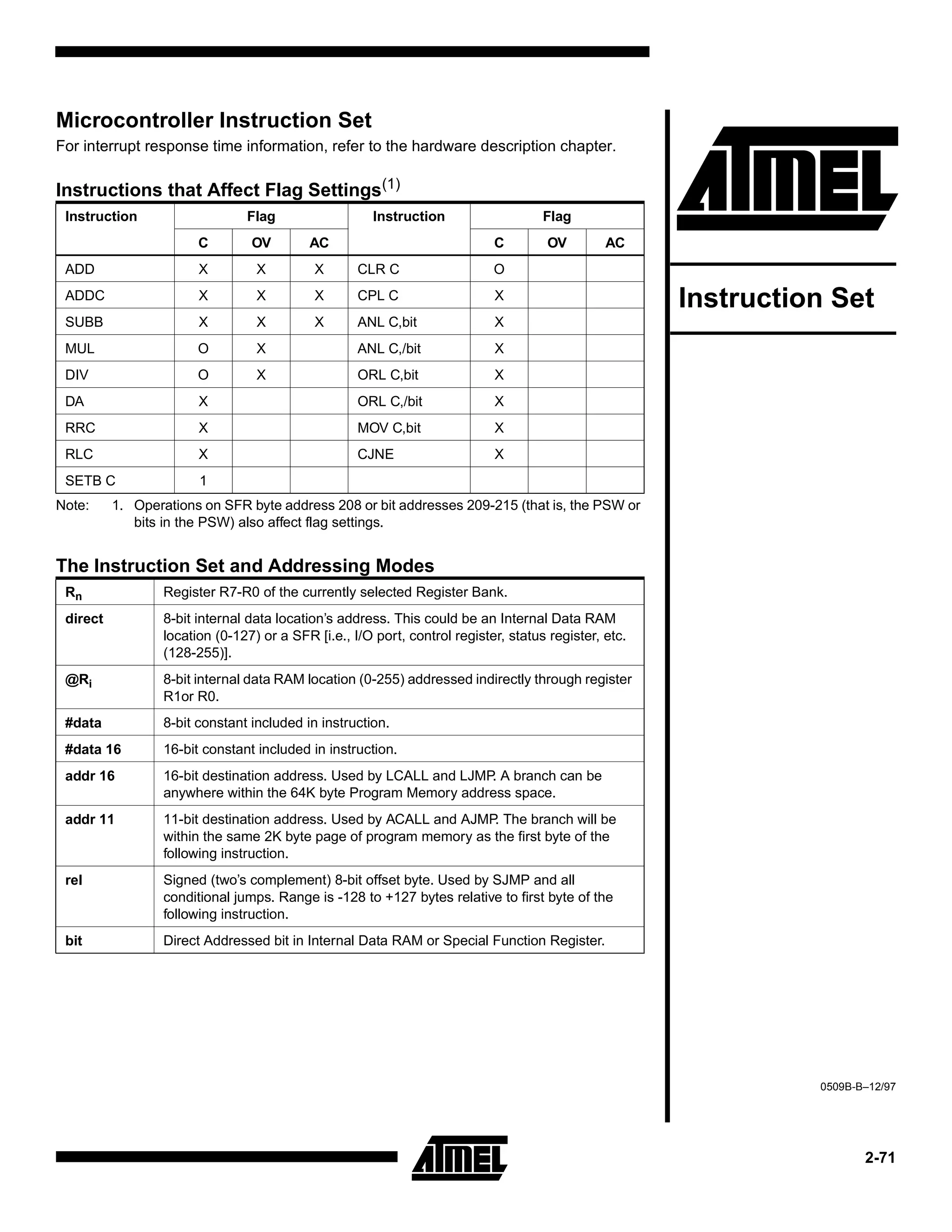
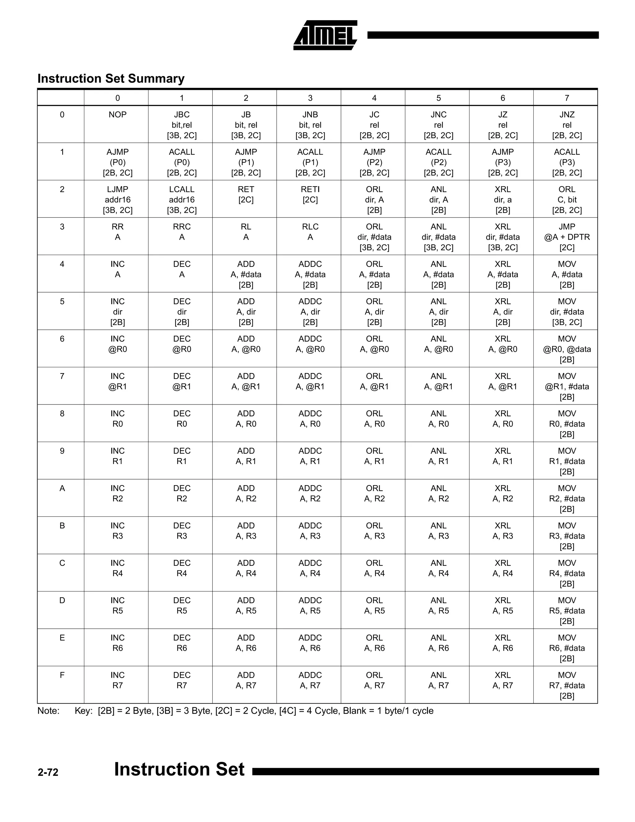
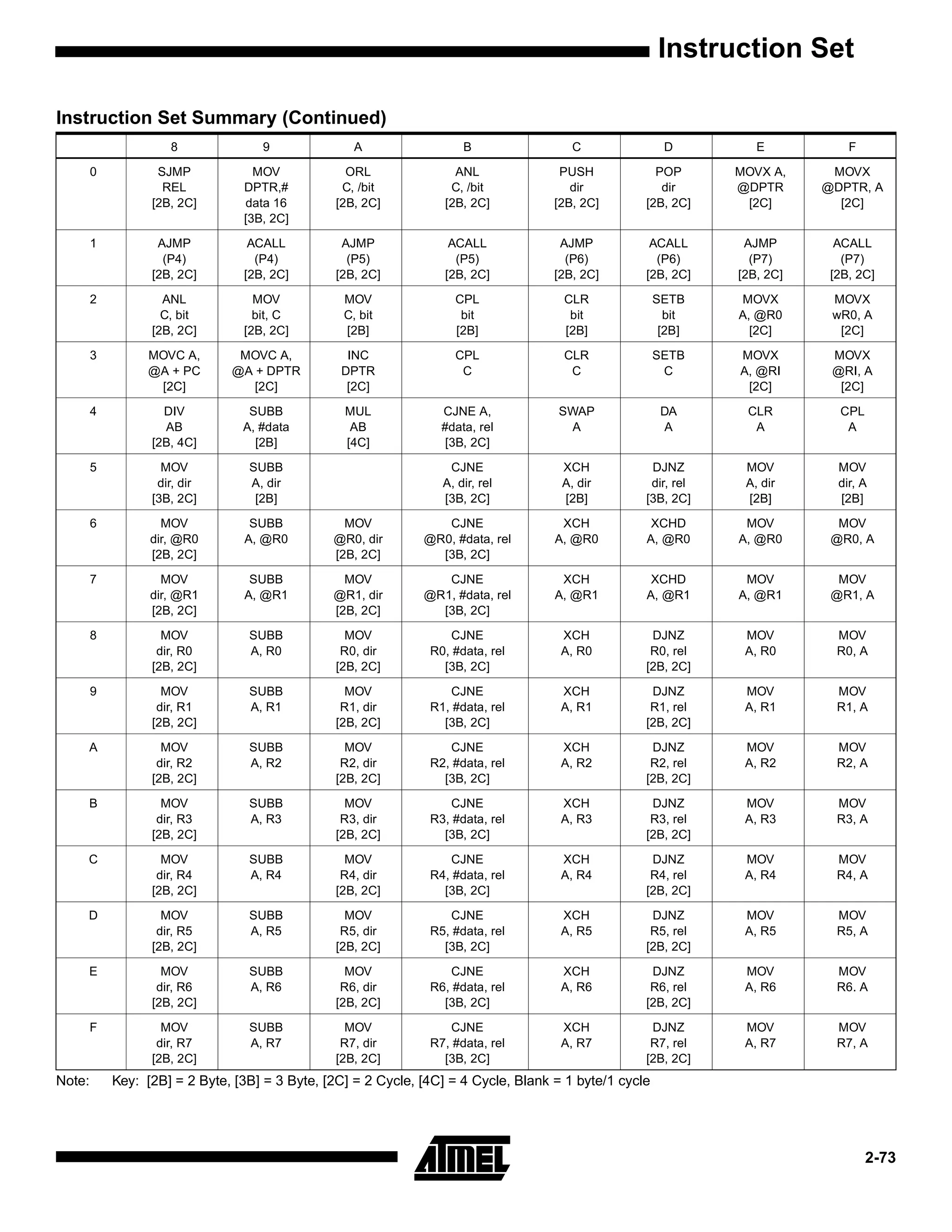
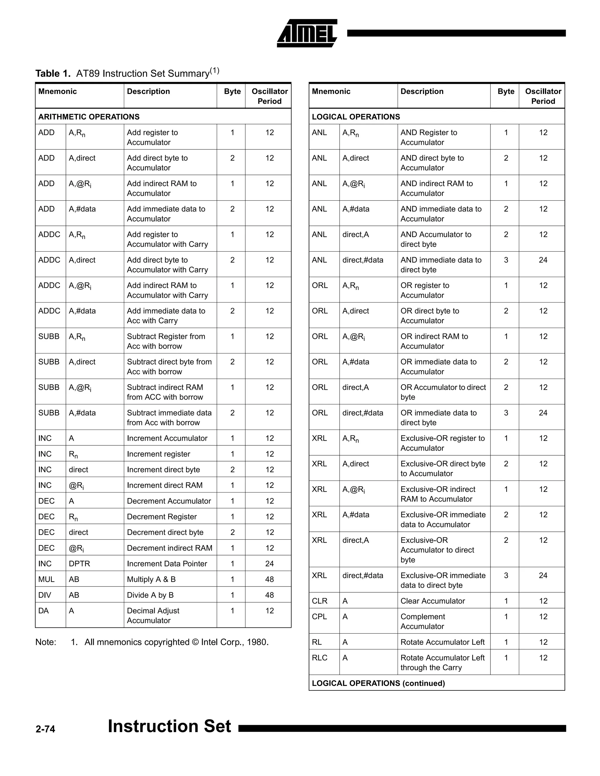
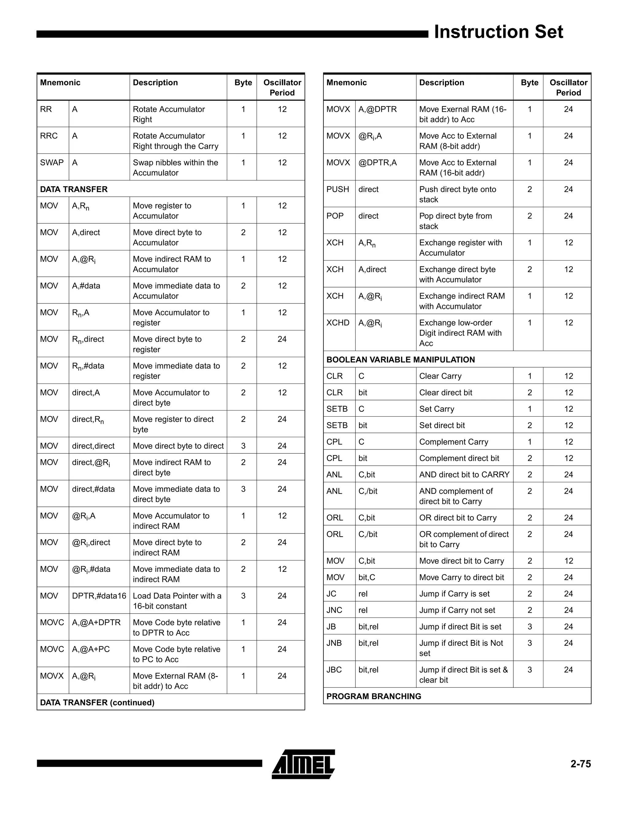
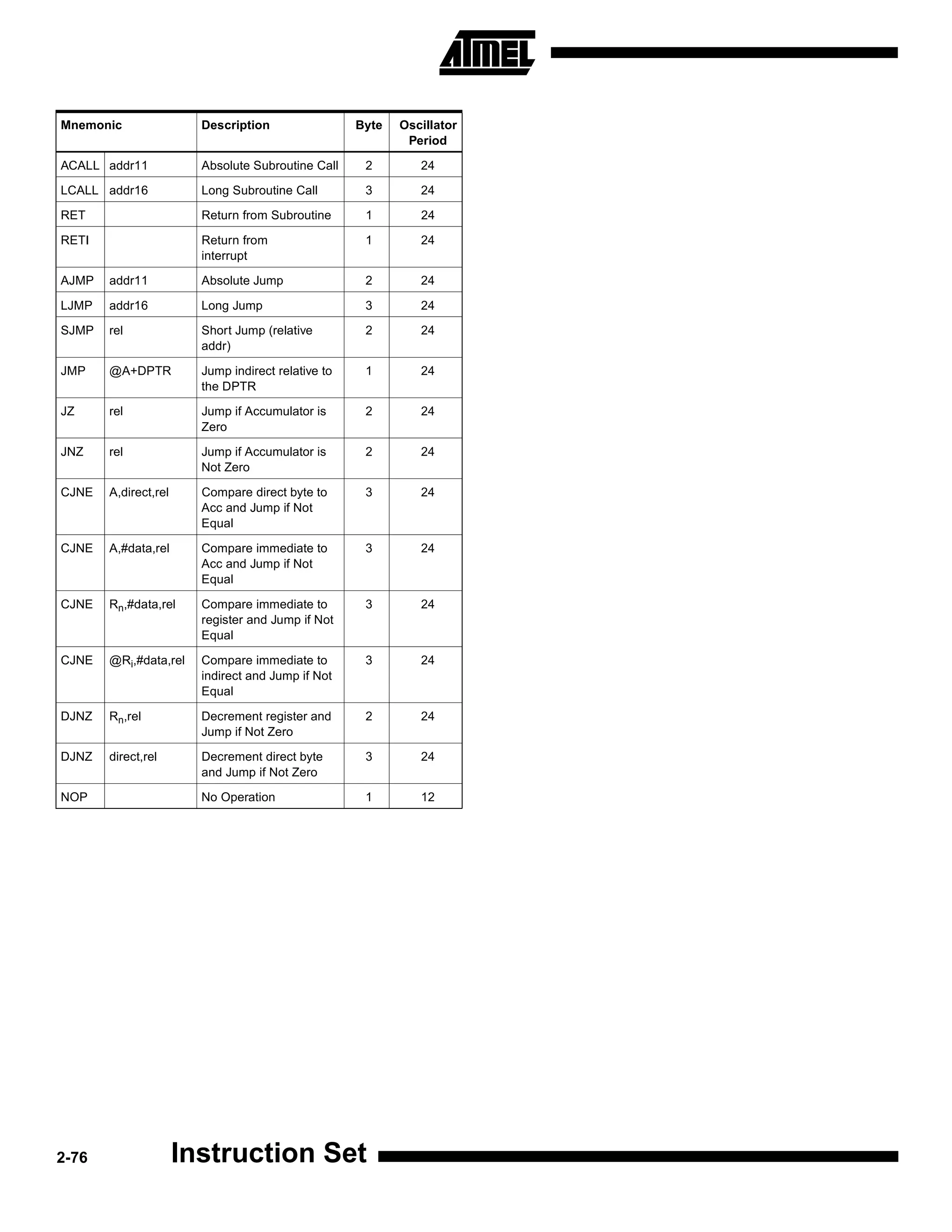
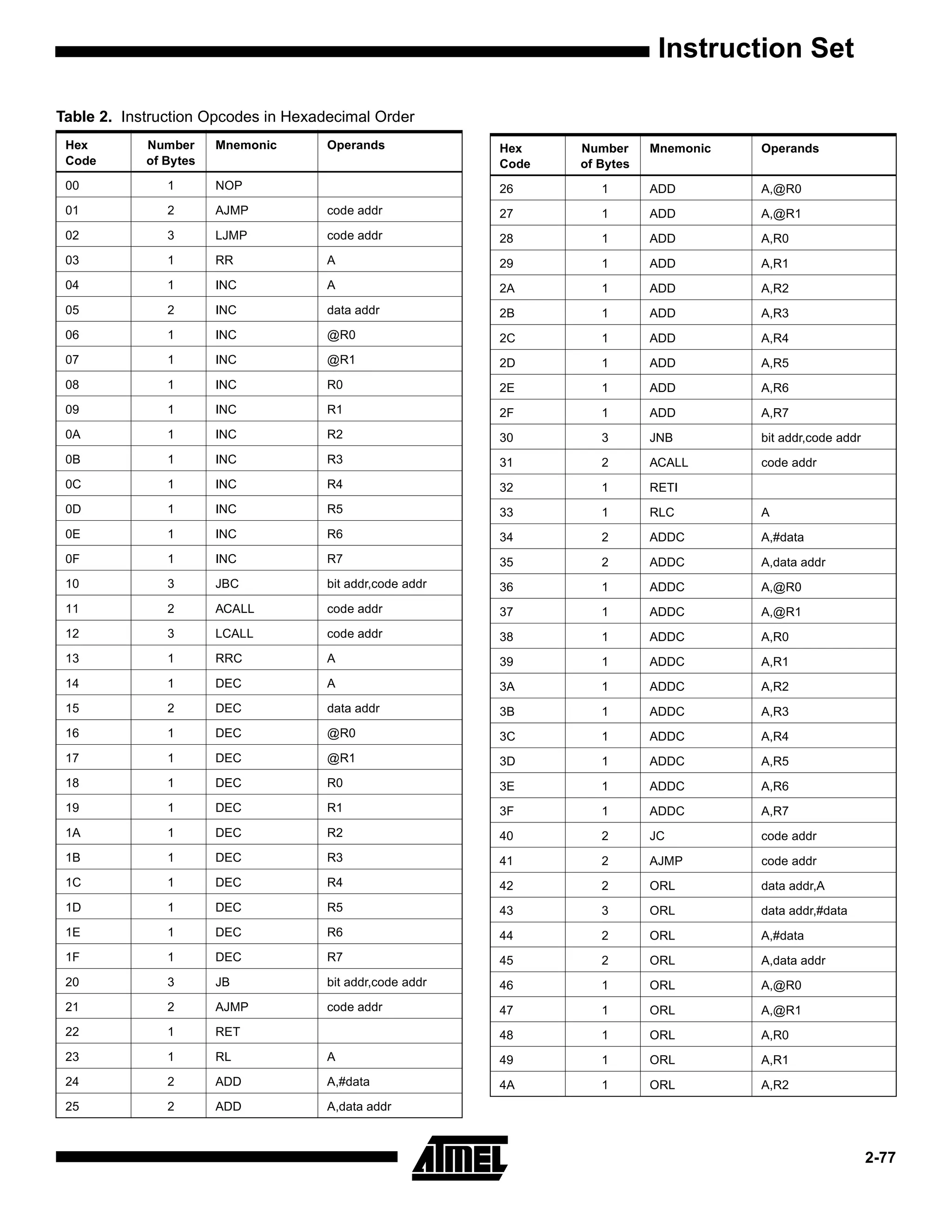
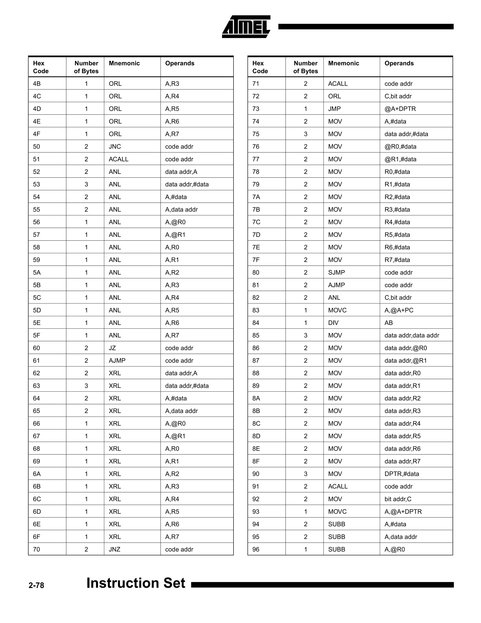
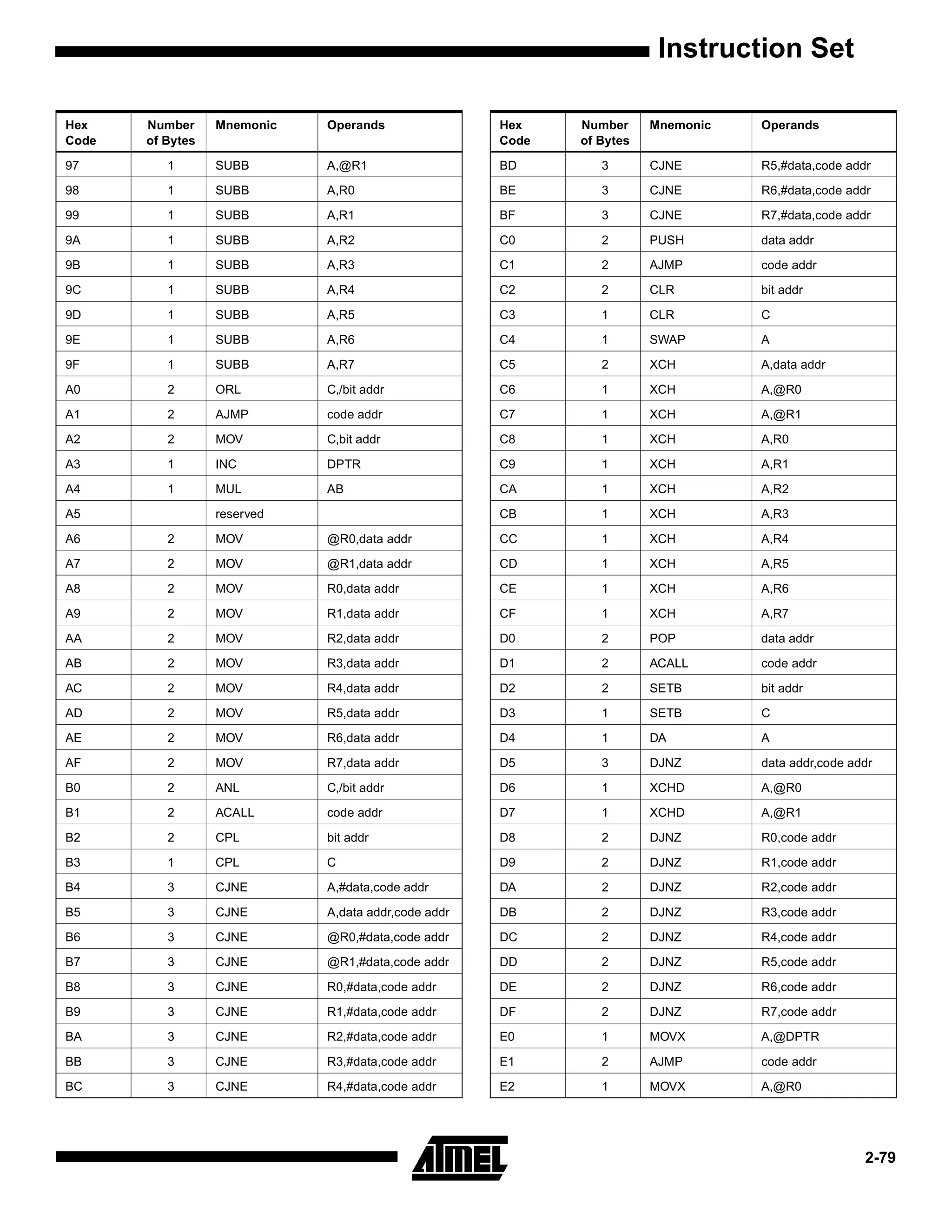
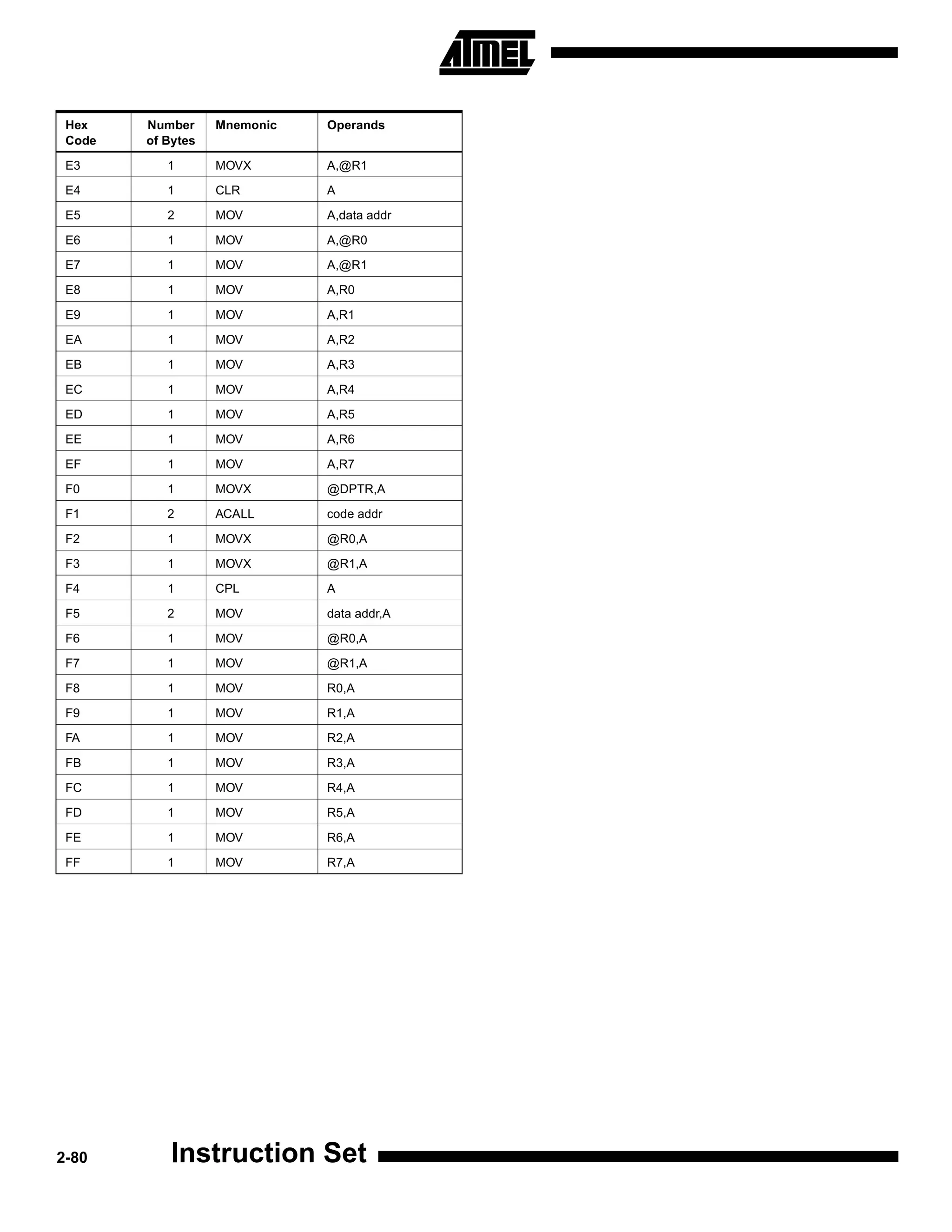
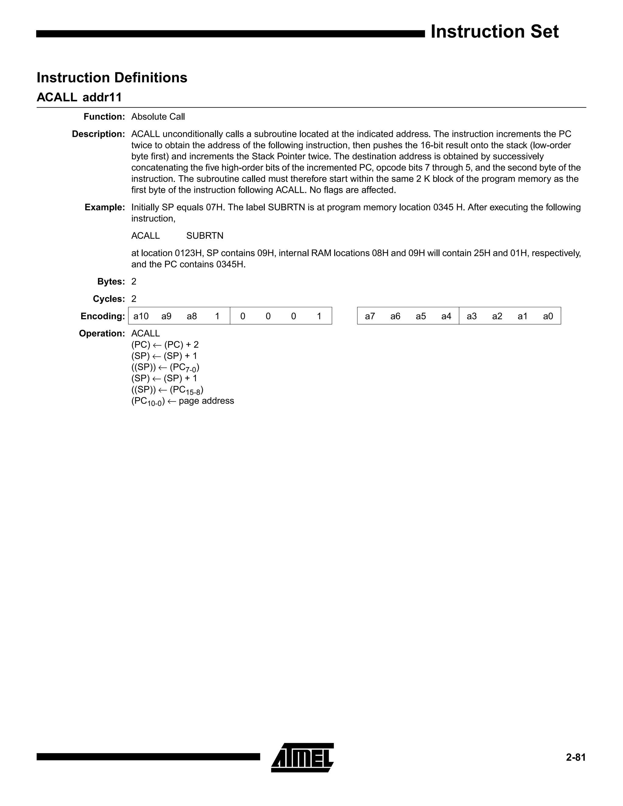
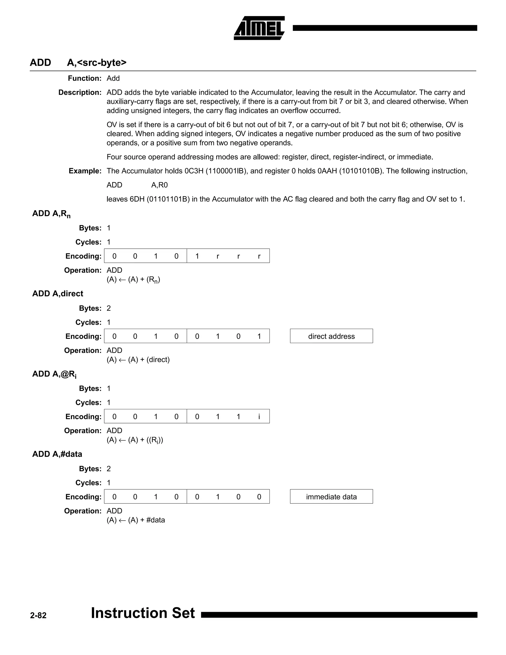
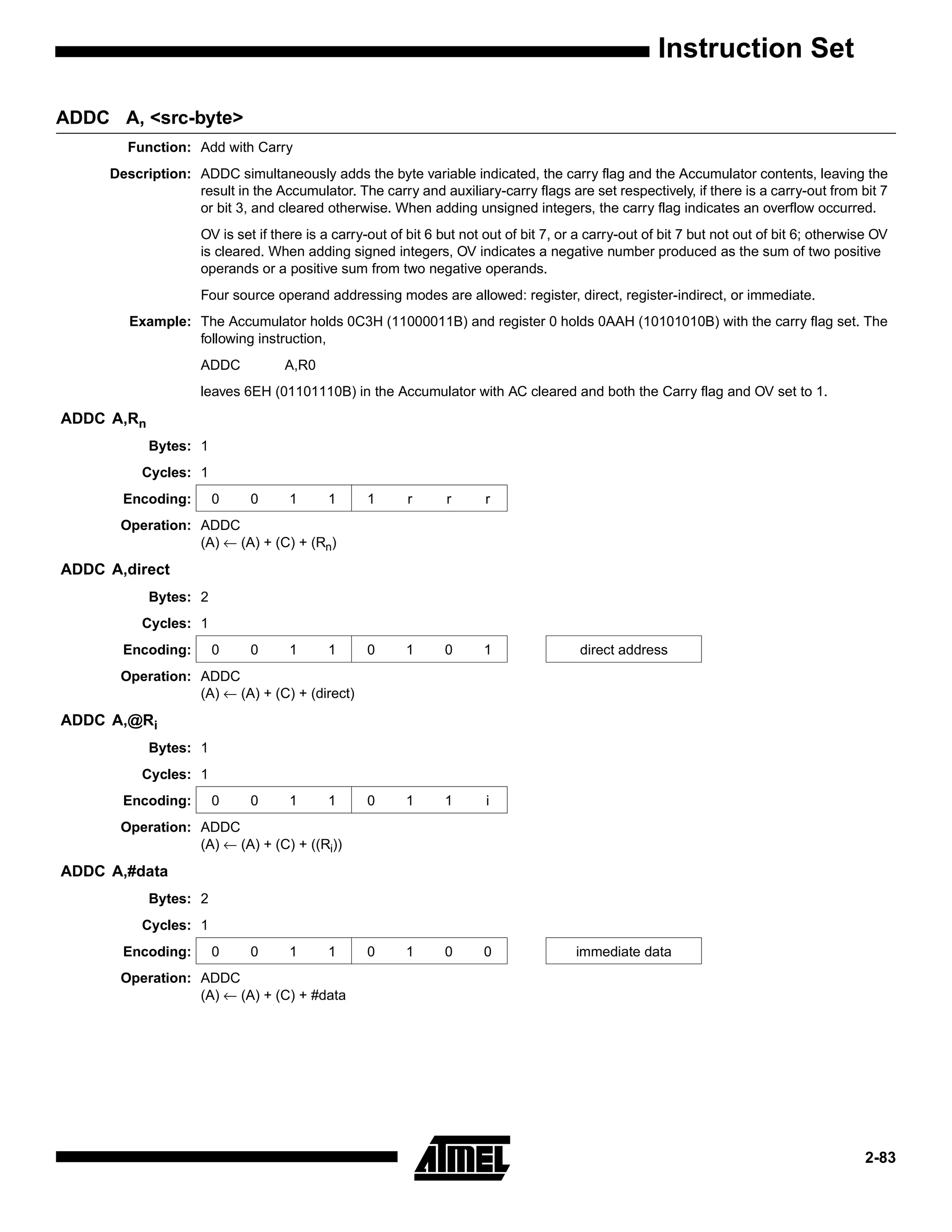
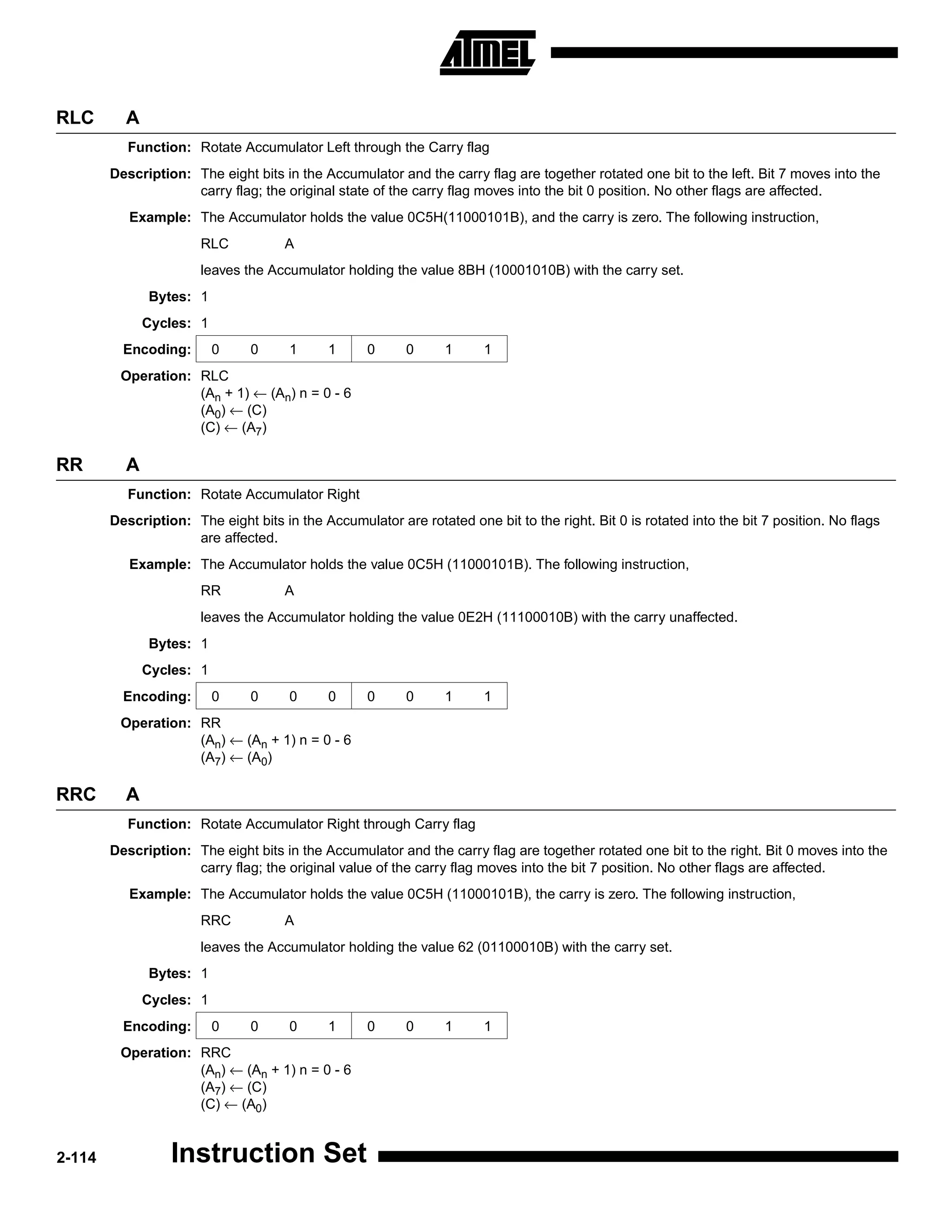
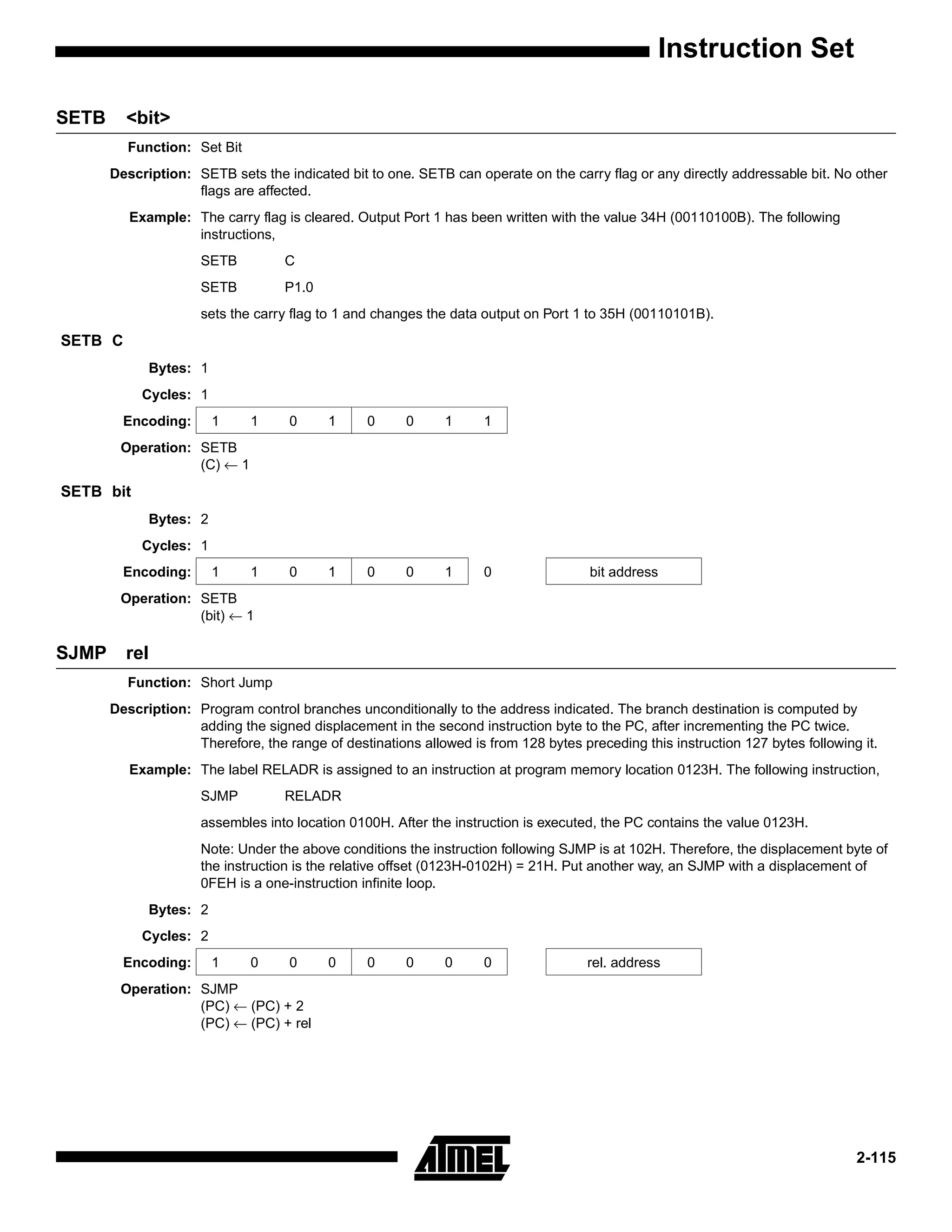
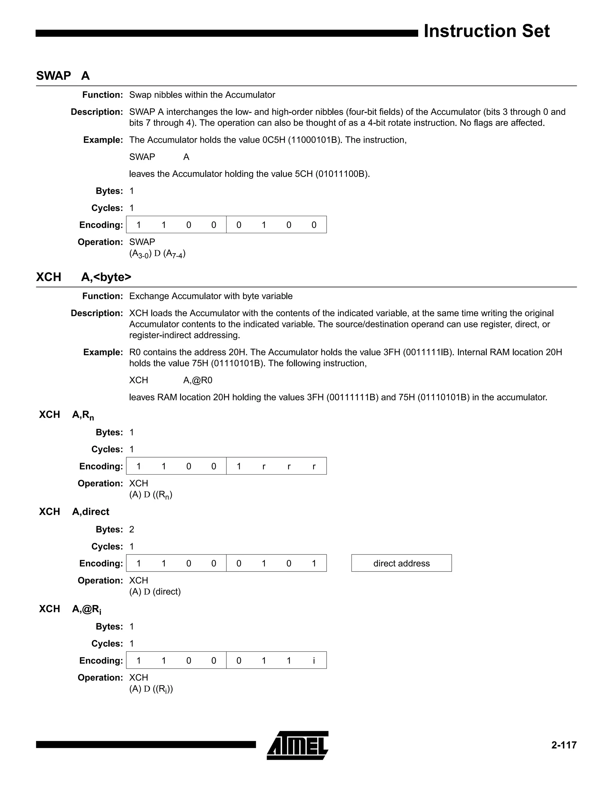
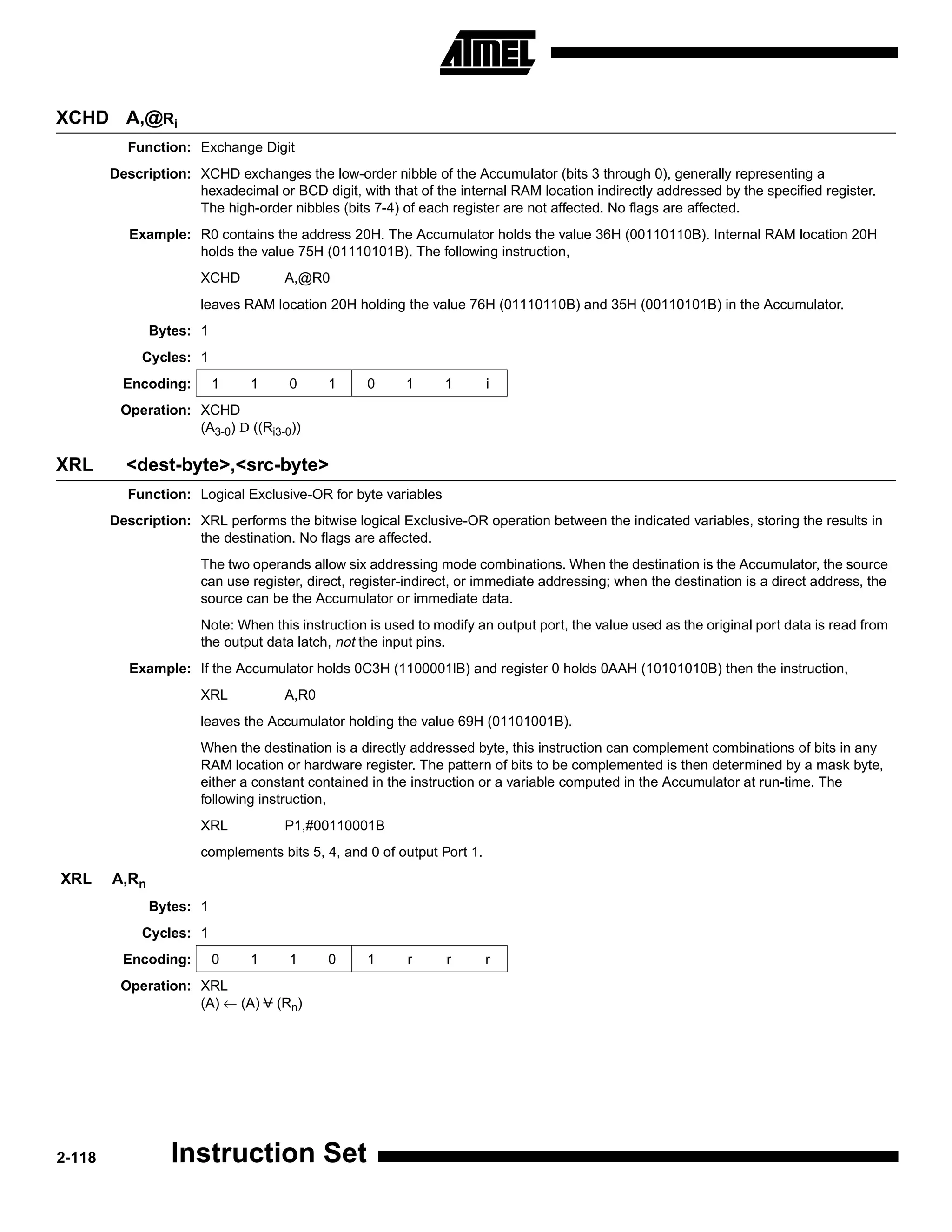
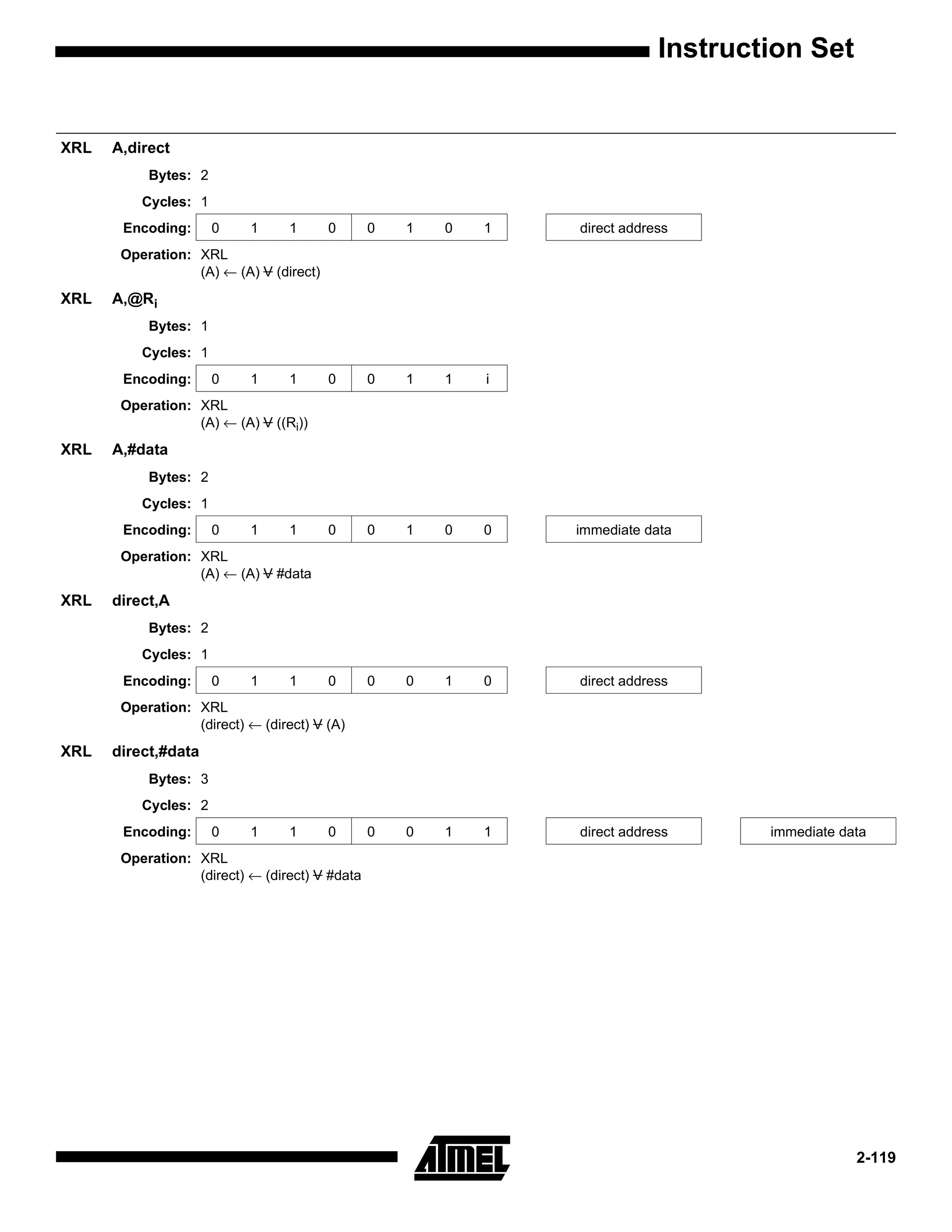
This document provides an instruction set summary for a microcontroller. It includes a table that lists each instruction, describes its function, and specifies the number of bytes in the instruction and its execution time in oscillator periods. It summarizes instructions related to arithmetic operations, logical operations, program flow control, bit manipulation, data transfer, and interrupts.
The document discusses programming the 8051 microcontroller. It can be programmed using low-level assembly language or high-level languages like C. Assembly language code is faster but more difficult to write and less portable, while C code is easier but slower. The document provides examples of adding two numbers in both C and assembly. It also discusses the 8051 instruction set, addressing modes, subroutines, and arithmetic operations.
The document discusses the Radix-2 discrete Fourier transform (DFT) algorithm. It explains that the Radix-2 DFT divides an N-point sequence into two N/2-point sequences, computes the DFT of each subsequence, and then combines the results to compute the N-point DFT. It involves decimating the sequence, computing smaller DFTs, and combining results over multiple stages. The Radix-2 algorithm reduces the computation from O(N^2) for the direct DFT to O(NlogN) operations.
The document discusses interrupts for the PIC18 microcontroller. It explains that interrupts allow the microcontroller to instantly respond to events like pin changes or timer overflows. When an interrupt occurs, the microcontroller stops executing the main program and jumps to the interrupt service routine (ISR) to handle the interrupt. It provides details on enabling and disabling interrupts, the interrupt vector table, and examples of using interrupts for external pins, timers, and serial communication.
This presentation gives the details about the data types available in Embedded C. It also discusses the pros and cons of writing codes in C for 8051. Different example codes are considered.
Describes ARM7-TDMI Processor Instruction Set. Explains classes of ARM7 instructions, syntax of data processing instructions, branch instructions, load-store instructions, coprocessor instructions, thumb state instructions.
The document discusses linear time-invariant (LTI) systems. It explains that:
1) The response of an LTI system to any input can be found by convolving the system's impulse response with the input. This is done using a convolution sum in discrete time and a convolution integral in continuous time.
2) Discrete-time signals and continuous-time signals can both be represented as weighted sums or integrals of shifted impulse functions.
3) For LTI systems, the impulse responses are simply time-shifted versions of the same underlying function, allowing the system to be fully characterized by its impulse response.
The document provides an overview of microprocessors and the 8085 microprocessor architecture. It discusses that a microprocessor is a programmable VLSI chip that includes an ALU, registers, and control circuits. The 8085 is an 8-bit microprocessor that can address 64KB of memory. It has three main functional blocks - a register array, ALU and logical group, and instruction decoder/timing and control circuitry. The document also describes the various registers, buses, pins and control signals of the 8085 microprocessor.
This document discusses tracking radar and monopulse radar. Tracking radar measures target coordinates to determine path and predict future locations. It tracks range, angle, Doppler, and velocity. Monopulse radar obtains angular location using simultaneous beams. It compares signals in sum and difference channels to obtain magnitude and direction of angular errors and keep the antenna pointed at the target. Amplitude comparison monopulse uses a hybrid junction to combine adjacent feeds into sum and difference signals. Phase comparison monopulse compares phase differences between signals from two antennas to determine angular errors.
The document discusses the memory organization and registers of the 8051 microcontroller. It describes the program memory and data memory, which are implemented using EPROM and RAM respectively. It then discusses the different registers of the 8051 including the accumulator, B register, data pointer register, stack pointer register, and special function registers. The special function registers are used for tasks like timer control and interrupt control.
The document contains multiple assembly language programs (ALPs) that perform operations like addition, finding minimum/maximum values, conversions between hexadecimal and ASCII, generating Fibonacci numbers, and calculating factorials and multiplication of numbers.
The document contains a list of 23 microprocessor lab programs and 6 interfacing programs for an electronics and communication course. The programs cover topics like data transfer, arithmetic operations, sorting, prime number generation, string operations, matrix multiplication and more. The document provides contents, program descriptions and assembly language code for some of the programs.
Attitude & orbital control system, TTC & M system, Power system, Communication subsystem, Satellite antenna, Space qualification, Equipment Reliability, redundancy
Linear block codes encode messages by adding parity bits to create codewords. They have the following properties:
1) They encode a k-bit message into an n-bit codeword, where n-k bits are parity bits calculated from the message bits.
2) Syndrome decoding uses the parity check matrix H to detect and locate errors by calculating the syndrome s, which depends only on the error pattern.
3) A linear block code can correct up to t errors per codeword if the minimum distance dmin is greater than 2t+1.
The document discusses various jump, loop, and call instructions for the 8051 microcontroller. It provides examples of using conditional and unconditional jumps to transfer program flow. Looping is achieved using decrement and jump if not zero instructions. Nested loops allow repeating an action more than 256 times. Subroutines are called using call instructions which save the return address on the stack. Parameters can be passed into subroutines using registers or push/pop instructions.
Radar Systems- Unit-III : MTI and Pulse Doppler RadarsVenkataRatnam14
This document provides an overview of moving target indication (MTI) and pulse Doppler radar systems. It describes the basic principles of MTI radar, including using Doppler shift to distinguish moving targets from clutter. It discusses different types of MTI radars and delay line cancellers. It also covers topics like blind speeds, staggered PRFs, range gated Doppler filters, and limitations to MTI performance. The key difference between MTI and pulse Doppler radar mentioned is that MTI radar operates with ambiguous Doppler but unambiguous range, while pulse Doppler radar has ambiguous range but unambiguous Doppler.
The document discusses interrupts in the 8085 microprocessor. It describes the concept of interrupts, where a peripheral device sends a signal to the CPU requesting attention. When an interrupt occurs, the CPU stops its current process and executes an interrupt service routine. There are three main types of interrupts - external, internal, and software interrupts. External interrupts are initiated by external devices, internal interrupts occur due to program errors, and software interrupts are initiated by executing an instruction. The document provides details on how interrupts are handled, including the interrupt acknowledge process, interrupt priorities, and methods for servicing multiple interrupts.
Assembler directives and basic steps ALP of 8086Urvashi Singh
The document discusses various assembler directives used in assembly language programming. It describes directives like DB, DW, DD, DQ, DT for data declaration; ASSUME to define logical segments; END, ENDP, ENDS to mark ends; EQU to define constants; PROC and ENDP to define procedures; ORG to set the location counter; SEGMENT to define logical segments; GROUP, INCLUDE, EVEN, and ALIGN for segment organization; EXTRN and PUBLIC for external references; and TYPE and PTR for defining variable types. The directives provide necessary information to the assembler to understand assembly language programs and generate machine code.
This document discusses amplitude modulation (AM) as a type of modulation used to transmit information signals. Modulation involves varying a high frequency carrier signal by an information signal in order to transmit the information signal over long distances. In AM, the amplitude of the carrier signal is varied in accordance with the instantaneous amplitude of the modulating or information signal. This creates two new sideband frequencies above and below the carrier frequency equal to the modulation frequency. The carrier and sidebands together make up the modulated signal. Only a portion of the transmitted power is present in the sidebands containing the information, while the rest is wasted in the carrier.
This document discusses arithmetic operations and conversions using the 8085 microprocessor. It includes algorithms and programs for 8-bit addition, subtraction, multiplication, and division. It also covers sorting algorithms to find the ascending and descending order of numbers, and algorithms to find the minimum and maximum numbers in a data set. Additionally, it explains programs that demonstrate the rotate instructions RLC, RRC, RAL, and RAR. Finally, it provides examples of conversions between ASCII, hexadecimal, and BCD codes.
The document discusses the architecture of the Intel 8085 microprocessor. It describes the 8085 as an 8-bit microprocessor introduced in 1976 that uses a single +5 volt power supply. The internal architecture includes a control unit, arithmetic logic unit (ALU), registers including the accumulator, program counter, stack pointer, instruction register/decoder, and timing and control unit. The document also briefly discusses interrupts, serial I/O, and some applications of microprocessors like mobile phones, watches, and appliances.
This document discusses different techniques for improving the quality of digitized signals, including companding, DPCM, and ADPCM. Companding uses non-uniform quantization to boost weak signals before quantization. DPCM transmits differences between actual and predicted sample values, reducing quantization noise. ADPCM further improves on DPCM with an adaptive quantizer that adjusts quantization step size based on prediction error. These methods allow higher quality digitization using fewer bits compared to basic uniform quantization.
This document provides an overview of analog to digital converters (ADCs) and describes how to interface the ADC0804 and ADC0808/0809 chips with an 8051 microcontroller. It discusses the basic functions and pinouts of the ADC0804 chip, how to convert analog voltages to digital values using its reference pin, and the steps to read output data. It also covers the channel selection, reference voltage, and programming steps for the 8-channel ADC0808/0809 chip. Timing diagrams are included to illustrate the read and write processes.
This document discusses elementary signals that are basic building blocks for more complex signals in signal and systems analysis. It identifies six types of elementary signals: unit step, unit ramp, unit parabolic, unit impulse, sinusoidal, and real exponential sequences. Each signal type is defined, with the unit step existing only for positive time, the unit ramp increasing linearly over time, the unit parabolic following a quadratic function, and the unit impulse being equal to one only at time zero. The document also notes that sinusoidal sequences can be periodic or not depending on frequency, and that real exponential sequences grow, decay, or alternate based on their constant value.
Addressing mode and instruction set using 8051logesh waran
Here are the key steps for programming timer 0 in mode 2:
1. Select mode 2 for timer 0 by writing to the TMOD register:
MOV TMOD,#02h
2. Write the initial count value to TH0:
MOV TH0,#0FCh
3. Clear the timer flag TF0:
CLR TF0
4. Start the timer by setting TR0:
SETB TR0
5. The timer will now count down from the value in TH0 (0FCh) to 0 in TL0.
6. When TL0 underflows to 0, TF0 will be set.
7. Check TF0 to detect overflow:
In communication system, intersymbol interference (ISI) is a form of distortion of a signal in which one symbol interferes with subsequent symbols. This is an unwanted phenomenon as the previous symbols have similar effect as noise, thus making the communication less reliable.
In communication system, the Nyquist ISI criterion describes the conditions which when satisfied by a communication channel (including responses of transmit and receive filters), result in no intersymbol interference(ISI). It provides a method for constructing band-limited functions to overcome the effects of intersymbol interference.
The document describes the instruction set of the Atmel 8051 microcontroller. It includes 3 tables that list the instructions, describing the operation, number of bytes in the instruction, and the oscillator period in cycles to execute the instruction. The tables provide a summary of arithmetic, logical, branch, and data transfer instructions available on the 8051 microcontroller.
This document describes the instruction set of the 8051 microcontroller, including arithmetic, logical, data transfer, program branching, and other instructions. It lists each instruction mnemonic, provides a brief description of its operation, and specifies the instruction size and number of clock cycles required. In total, over 50 different instructions are outlined pertaining to common operations like addition, logical operations, movement of data, jumps, and flags manipulation.
The instruction set of the microcontroller includes arithmetic, logical, and flag-affecting instructions. It allows operations on registers, direct addresses, and indirect addresses. The instruction byte size and oscillator period required for each instruction is also provided in a table.
The instruction set of the microcontroller includes arithmetic, logical, and flag-affecting instructions. It allows operations on registers, direct addresses, and indirect addresses. Common instructions include ADD, SUB, AND, OR, MOV, JMP, CALL. The instruction set supports conditional jumps based on flag settings from previous operations. Most instructions execute in 1 byte and 1 cycle.
The document provides information about a microcontroller instruction set including:
- Instructions that affect flag settings and how they modify the flags.
- The instruction set and addressing modes which include registers, direct addressing, indirect addressing, constants, and branches.
- A summary of the instruction set organized in a table with the opcode, instruction name, addressing mode, and byte size/cycle information.
The instruction set summary provides concise information about the instructions of the AT89 microcontroller in a tabular format. The table lists instructions according to operation type and describes each instruction's mnemonic, operation performed, byte size, and oscillator period. A second table continues listing additional instructions.
This document provides information about the instruction set of a microcontroller. It includes two summaries:
1. The first summary lists instructions and describes how they affect flag settings in the microcontroller's status register, such as the carry and overflow flags.
2. The second summary is a table that provides details about the microcontroller's instruction set. It lists instructions, describes their operation, and specifies the number of bytes and oscillator periods each instruction requires. The table is divided into sections for arithmetic, logical, branching, and other operations.
The document as a whole provides low-level technical specifications about a microcontroller's instruction set, including how instructions are encoded, how they modify status register flags, and their timing
This document describes the instruction set of the 8051 microcontroller. It discusses the three types of instructions - single byte, double byte, and triple byte - based on the number of bytes needed to represent the instruction. It provides examples of different types of instructions, including data transfer, arithmetic, logical, logical bit, and program flow control instructions. Each instruction is defined by its mnemonic, description, and number of bytes.
The document discusses different addressing modes in 8051 microcontroller - immediate, register, direct, register indirect and indexed addressing. It provides examples of instructions using each addressing mode like MOV, ADD etc. and explains how the address is specified directly or indirectly using registers in each mode.
microcontroller_instruction_set for ENGINEERING STUDENTSssuser2b759d
The document discusses the instruction set of microcontrollers. It describes that microcontrollers have instruction formats that specify the operation and operands. The 8051 microcontroller has 111 instructions divided into one-byte, two-byte, and three-byte instructions depending on the number of bytes needed to represent the instruction. The document outlines the different addressing modes and types of instructions including data transfer, arithmetic, logical, and program flow control instructions. It provides examples of common instructions and their operation.
The microcontroller instruction set includes instructions for flow control, logic, arithmetic, and data movement. It supports operations on registers and direct or indirect addressed memory locations. The instruction set is encoded in an 8-bit format and includes operations that affect the processor status flags.
The document discusses the addressing modes, instruction set, and assembly language programming of the 8051 microcontroller. It describes the five addressing modes of 8051 - immediate, direct, register, register indirect, and indexed addressing modes. It also explains some common arithmetic, logical, and other instructions like ADD, AND, OR, XOR, INC, DEC etc. and provides examples of using these instructions to manipulate data in registers and memory locations.
The document discusses various addressing modes and instructions of the 8051 microcontroller. It describes the five addressing modes - immediate, register, direct, register indirect and indexed. It explains each addressing mode in detail. It also explains the various instruction groups - data transfer, arithmetic, logical, boolean and branching instructions. It provides examples of instructions like MOV, ADD, ANL, JMP etc. and how they are used to manipulate data in the 8051.
The document discusses various aspects of the 8051 microcontroller such as instruction types, addressing modes, RAM space allocation, and instruction sets. It explains that 8051 instructions are divided into one-byte, two-byte, and three-byte instructions depending on the number of bytes required to represent them. It describes the five addressing modes - register, direct, indirect, immediate, and index. It also provides examples of different instruction types like data transfer, arithmetic, logical, and branching instructions.
The document provides information about microcontrollers and the 8051 microcontroller family. It defines a microcontroller as a programmable digital processor with on-chip memory and peripherals. It then compares microcontrollers to microprocessors, noting that microcontrollers have on-chip memory and peripherals while microprocessors require external memory. The document proceeds to discuss the development and classification of microcontrollers like the Intel 4004 and 8051. It provides details on the architecture, memory structure, instructions, and I/O ports of the 8051 microcontroller.
The document summarizes key aspects of the ARM instruction set architecture including:
- ARM instructions are 32-bit and there are 232 possible instructions defined.
- ARM uses a load-store architecture with 3-address instructions and conditional execution.
- The instruction set supports data processing, data movement, and flow control instructions. Data processing instructions support register, immediate, and shifted register operands.
The document discusses numerical bases used in programming such as hexadecimal, binary, and BCD. It provides examples of converting between decimal, binary, hexadecimal and BCD representations of numbers. It also summarizes common registers, memory mapping, addressing modes, and basic instructions of the 8051 microcontroller.
This document provides an overview of the ARM instruction set architecture. It discusses the ARM programming model including its general purpose registers and status flags. It also covers ARM data types, data operations, load/store instructions, flow of control instructions, and subroutine calling conventions. Examples are provided to demonstrate how common programming constructs like if/else statements and for loops can be implemented in ARM assembly language.
The Microprocessor System. A semester course review. Summarize important points for whole subject. Using the 8051 architecture as the practical and projects development.
The document discusses numerical bases used in programming such as hexadecimal, binary, and BCD. It provides examples of converting between decimal, binary, hexadecimal and BCD representations of numbers. It also describes registers and memory organization in 8051 microcontrollers including register banks, memory mapping, and addressing modes. Finally, it outlines common instructions of the 8051 instruction set such as MOV, ADD, CALL, JUMP, LOGICAL operations and flag manipulation.
This lab assignment asks students to:
1. Write assembly code to generate square waveforms of specific frequencies corresponding to musical notes, as indicated in Table 1, and output these to P0.7 based on switch input. Students are to verify this works using simulation before the lab.
2. During the lab, connect a speaker to the microprocessor kit using the provided circuit diagram to interface the speaker. Students should then be able to play notes by changing the switch positions and hearing sound from the speaker.
3. Teaching assistants will check that the correct waveforms are being generated and the speaker interfacing is working properly for different switch inputs.
This document provides instructions for Lab 1 of the Microprocessors Laboratory course. It is worth 20 points and has two parts. The first part (10 points) involves downloading a program, debugging it to fix errors, and running it successfully. The second part (10 points) uses the corrected program and involves debugging step-by-step without functions, setting a breakpoint, modifying memory locations, and using logic analysis to find the frequency output on Port1. The TA is instructed to check that students have completed each step correctly, including creating projects, compiling code, modifying memory, using breakpoints, and examining registers.
- This document outlines the course details for the EE337 Microprocessors Lab course, including instructors, timings, objectives, skills gained, prerequisites, grading policy, attendance policy, lab experiment schedule, evaluation process, reference texts, software, and download links.
- The course aims to develop applications on the 8051 microcontroller and complements the Microprocessor theory course. Students will write programs, interface peripherals, and implement communication protocols.
- Labs will be evaluated weekly on Mondays or Tuesdays depending on student schedule. Strict policies are in place for attendance, submissions, academic dishonesty, and board usage. Students will receive an 8051 development board and are responsible for its care.
This document outlines the course details for the EE337 - Microprocessors Lab course. The objectives are to understand and develop applications for the 8051 microcontroller and complement the Microprocessor theory course. Students will gain skills in developing, simulating, and debugging programs using an IDE and writing assembly and embedded C programs. The course will be graded based on lab experiments, assignments, and a final project. Students will complete approximately 8 labs and show their work to an assigned TA. Prerequisites for the course and required software and development board are also outlined.
The document provides instructions for using the PT-51 microcontroller board. The board features an Atmel AT89C5131A microcontroller, LEDs, switches, and connectors for LCD, SPI, and I2C. It can be programmed via USB in bootloader mode by holding the Boot and Reset buttons while toggling the USB switch. Users install Keil uVision and Flip to write, compile, and load HEX files. The board runs code in application mode and enters bootloader mode to receive new programs.
This document contains instructions for Assignment 1 of the Microprocessors Laboratory course. It has two parts worth a total of 20 points. The first part (5 points) requires writing a program to count the number of set bits in a byte and store the result in another location. The second part (15 points) requires finding the largest and second largest numbers from a list of 20 integers and storing the results in two specified locations, using subtraction to compare integers. The document also lists 9 checkpoints for the teaching assistant to verify the student's understanding of using Keil uVision to write, compile, debug, and run assembly language programs.
This document provides instructions for Lab 1 of the Microprocessors Laboratory course. It consists of two parts worth 20 points total:
1. Write an assembly program to add two 8-bit numbers in memory locations 70H and 71H and store the result in 72H, with the carry flag in 73H.
2. Write an assembly program to encode 16 bits from 70H-71H into 4 Hamming codewords using a (7,4) code, and store the results in 72H-75H. The document also provides checkpoints for teaching assistants to verify students' understanding of developing and debugging assembly programs.
The document provides an overview of how to get started using the Keil μVision IDE for embedded development. It describes the key components of an IDE like Keil μVision, including the editor, compiler, debugger and downloader. It then walks through setting up a sample project for a Microchip AT89C5131A microcontroller, adding and compiling code files, and debugging the built program. It also provides tips for solving issues like crashes that may occur when debugging.
This document provides an outline for the EE337 Microprocessors Lab course. The course objectives are to understand and develop applications for the 8051 microcontroller and complement the Microprocessor theory course. Students will gain skills in developing, simulating, and debugging programs using an IDE, and writing assembly and embedded C programs to interface peripherals like LCDs and keypads. Prerequisites include digital circuits and systems courses. Labs will make up 60% of the grade, with assignments and a project accounting for the rest. The course will use an online platform and kits containing development boards will be provided to students.
This document discusses using Keil uVision IDE to create hex files for programming microcontrollers. It covers creating and configuring projects in Keil uVision, adding and compiling source code files, and generating hex files. Key aspects include setting up the microcontroller target options, rebuilding code to generate machine code and check for errors, and programming the microcontroller with the hex file. The goal is to provide an integrated workflow for coding, compiling, and programming microcontrollers using Keil's IDE.
Keil uVision is an integrated development environment (IDE) that provides a single solution for coding, building, debugging and flashing programs onto microcontrollers. The debugger in Keil uVision allows users to observe registers, memory, ports and peripherals, set breakpoints, monitor code execution and modify variables. It displays the disassembly code, assembly/high level code, registers and memory to help debug programs on a simulator.
- Serial communication involves transmitting data one bit at a time over a single wire, using shift registers at the transmitter and receiver. This allows data to be sent over long distances or inherently single-wire mediums like phone lines.
- For asynchronous serial communication, start and stop bits are used to synchronize the transmitter and receiver clocks, since they have small mismatches. This results in a 10-bit frame structure.
- The 8051 microcontroller has built-in support for serial communication through its SBUF register and SCON configuration register. It can implement both synchronous and asynchronous serial protocols for transmitting and receiving serial data.
The document discusses timers in the 8051 microcontroller. It covers the following key points:
- The 8051 has two timers, T0 and T1, that can be configured as event counters or timers.
- Special function registers are used to control the timers' modes, counts, flags, and interrupts.
- Timers count up and set flags when they overflow from their maximum count to 0.
- Interrupts must be enabled for the timers and their overflow flags to trigger an interrupt service routine.
- Reading the two bytes that make up a timer's count requires care to avoid inconsistencies due to the counter changing between reads.
The document summarizes interrupts in the 8051 microcontroller. It discusses the five interrupt sources - two external interrupt lines, two timers, and the serial interface. It describes how to enable interrupts from these sources by setting bits in the interrupt enable register. It also discusses interrupt priorities, vector addresses, and the sequence of events that occurs when an interrupt is triggered and then returned from.
The document provides an introduction to microcontrollers. It discusses the need for programmable devices and how microcontrollers address this need by allowing their function to be selected through digital inputs. Microcontrollers contain a processor that can run programs stored in memory and contain registers used for tasks like instruction fetching. The document then describes the Von Neumann and Harvard architectures, instruction fetching, decoding, and execution processes, and how interrupts can alter program flow. It concludes by discussing the 8051 microcontroller architecture in detail, including its memory organization, registers, addressing modes, and notation.
This document describes the features and specifications of an 8-bit microcontroller with full-speed USB capabilities. It includes an 80C52 core, 16/32KB flash memory, 1KB SRAM, timers, serial communication interfaces, and a full-speed USB module compatible with USB 1.1 and 2.0 specifications. The microcontroller has low power idle and power-down modes and an operating temperature range of industrial levels. It comes in 52-pin PLCC, 64-pin VQFP, and 32-pin QFN packages.
The document provides operating instructions for the Pt-51 microcontroller board. It describes the board specifications including the AT89C5131A microcontroller, crystal clock, LEDs, switches, and USB connector. It explains how to install the necessary software, use the board in bootloader mode to load programs using Atmel Flip, and run programs in application mode.
This document outlines the course details for EE337 - Microprocessors Lab. The objectives of the course are to understand and develop applications on a microcontroller, complementing the theory covered in EE309. Students will gain skills in using an IDE for developing, simulating and debugging programs, as well as writing assembly and embedded C programs and interfacing peripherals. The course will involve 8-10 independent lab experiments using a PT-51 development board. Students must maintain a lab book, install the necessary software, and will be graded based on their lab session performance, three exams, and a completed lab book. Assistance is available from TAs and instructors.
Building a Raspberry Pi Robot with Dot NET 8, Blazor and SignalRPeter Gallagher
In this session delivered at NDC Oslo 2024, I talk about how you can control a 3D printed Robot Arm with a Raspberry Pi, .NET 8, Blazor and SignalR.
I also show how you can use a Unity app on an Meta Quest 3 to control the arm VR too.
You can find the GitHub repo and workshop instructions here;
https://bit.ly/dotnetrobotgithub
Google Calendar is a versatile tool that allows users to manage their schedules and events effectively. With Google Calendar, you can create and organize calendars, set reminders for important events, and share your calendars with others. It also provides features like creating events, inviting attendees, and accessing your calendar from mobile devices. Additionally, Google Calendar allows you to embed calendars in websites or platforms like SlideShare, making it easier for others to view and interact with your schedules.
1. 2-71
Microcontroller Instruction Set
For interrupt response time information, refer to the hardware description chapter.
Note: 1. Operations on SFR byte address 208 or bit addresses 209-215 (that is, the PSW or
bits in the PSW) also affect flag settings.
Instructions that Affect Flag Settings(1)
Instruction Flag Instruction Flag
C OV AC C OV AC
ADD X X X CLR C O
ADDC X X X CPL C X
SUBB X X X ANL C,bit X
MUL O X ANL C,/bit X
DIV O X ORL C,bit X
DA X ORL C,/bit X
RRC X MOV C,bit X
RLC X CJNE X
SETB C 1
The Instruction Set and Addressing Modes
Rn Register R7-R0 of the currently selected Register Bank.
direct 8-bit internal data location’s address. This could be an Internal Data RAM
location (0-127) or a SFR [i.e., I/O port, control register, status register, etc.
(128-255)].
@Ri 8-bit internal data RAM location (0-255) addressed indirectly through register
R1or R0.
#data 8-bit constant included in instruction.
#data 16 16-bit constant included in instruction.
addr 16 16-bit destination address. Used by LCALL and LJMP. A branch can be
anywhere within the 64K byte Program Memory address space.
addr 11 11-bit destination address. Used by ACALL and AJMP. The branch will be
within the same 2K byte page of program memory as the first byte of the
following instruction.
rel Signed (two’s complement) 8-bit offset byte. Used by SJMP and all
conditional jumps. Range is -128 to +127 bytes relative to first byte of the
following instruction.
bit Direct Addressed bit in Internal Data RAM or Special Function Register.
0509B-B–12/97
Instruction Set
2. Instruction Set2-72
Instruction Set Summary
Note: Key: [2B] = 2 Byte, [3B] = 3 Byte, [2C] = 2 Cycle, [4C] = 4 Cycle, Blank = 1 byte/1 cycle
0 1 2 3 4 5 6 7
0 NOP JBC
bit,rel
[3B, 2C]
JB
bit, rel
[3B, 2C]
JNB
bit, rel
[3B, 2C]
JC
rel
[2B, 2C]
JNC
rel
[2B, 2C]
JZ
rel
[2B, 2C]
JNZ
rel
[2B, 2C]
1 AJMP
(P0)
[2B, 2C]
ACALL
(P0)
[2B, 2C]
AJMP
(P1)
[2B, 2C]
ACALL
(P1)
[2B, 2C]
AJMP
(P2)
[2B, 2C]
ACALL
(P2)
[2B, 2C]
AJMP
(P3)
[2B, 2C]
ACALL
(P3)
[2B, 2C]
2 LJMP
addr16
[3B, 2C]
LCALL
addr16
[3B, 2C]
RET
[2C]
RETI
[2C]
ORL
dir, A
[2B]
ANL
dir, A
[2B]
XRL
dir, a
[2B]
ORL
C, bit
[2B, 2C]
3 RR
A
RRC
A
RL
A
RLC
A
ORL
dir, #data
[3B, 2C]
ANL
dir, #data
[3B, 2C]
XRL
dir, #data
[3B, 2C]
JMP
@A + DPTR
[2C]
4 INC
A
DEC
A
ADD
A, #data
[2B]
ADDC
A, #data
[2B]
ORL
A, #data
[2B]
ANL
A, #data
[2B]
XRL
A, #data
[2B]
MOV
A, #data
[2B]
5 INC
dir
[2B]
DEC
dir
[2B]
ADD
A, dir
[2B]
ADDC
A, dir
[2B]
ORL
A, dir
[2B]
ANL
A, dir
[2B]
XRL
A, dir
[2B]
MOV
dir, #data
[3B, 2C]
6 INC
@R0
DEC
@R0
ADD
A, @R0
ADDC
A, @R0
ORL
A, @R0
ANL
A, @R0
XRL
A, @R0
MOV
@R0, @data
[2B]
7 INC
@R1
DEC
@R1
ADD
A, @R1
ADDC
A, @R1
ORL
A, @R1
ANL
A, @R1
XRL
A, @R1
MOV
@R1, #data
[2B]
8 INC
R0
DEC
R0
ADD
A, R0
ADDC
A, R0
ORL
A, R0
ANL
A, R0
XRL
A, R0
MOV
R0, #data
[2B]
9 INC
R1
DEC
R1
ADD
A, R1
ADDC
A, R1
ORL
A, R1
ANL
A, R1
XRL
A, R1
MOV
R1, #data
[2B]
A INC
R2
DEC
R2
ADD
A, R2
ADDC
A, R2
ORL
A, R2
ANL
A, R2
XRL
A, R2
MOV
R2, #data
[2B]
B INC
R3
DEC
R3
ADD
A, R3
ADDC
A, R3
ORL
A, R3
ANL
A, R3
XRL
A, R3
MOV
R3, #data
[2B]
C INC
R4
DEC
R4
ADD
A, R4
ADDC
A, R4
ORL
A, R4
ANL
A, R4
XRL
A, R4
MOV
R4, #data
[2B]
D INC
R5
DEC
R5
ADD
A, R5
ADDC
A, R5
ORL
A, R5
ANL
A, R5
XRL
A, R5
MOV
R5, #data
[2B]
E INC
R6
DEC
R6
ADD
A, R6
ADDC
A, R6
ORL
A, R6
ANL
A, R6
XRL
A, R6
MOV
R6, #data
[2B]
F INC
R7
DEC
R7
ADD
A, R7
ADDC
A, R7
ORL
A, R7
ANL
A, R7
XRL
A, R7
MOV
R7, #data
[2B]
3. Instruction Set
2-73
Instruction Set Summary (Continued)
Note: Key: [2B] = 2 Byte, [3B] = 3 Byte, [2C] = 2 Cycle, [4C] = 4 Cycle, Blank = 1 byte/1 cycle
8 9 A B C D E F
0 SJMP
REL
[2B, 2C]
MOV
DPTR,#
data 16
[3B, 2C]
ORL
C, /bit
[2B, 2C]
ANL
C, /bit
[2B, 2C]
PUSH
dir
[2B, 2C]
POP
dir
[2B, 2C]
MOVX A,
@DPTR
[2C]
MOVX
@DPTR, A
[2C]
1 AJMP
(P4)
[2B, 2C]
ACALL
(P4)
[2B, 2C]
AJMP
(P5)
[2B, 2C]
ACALL
(P5)
[2B, 2C]
AJMP
(P6)
[2B, 2C]
ACALL
(P6)
[2B, 2C]
AJMP
(P7)
[2B, 2C]
ACALL
(P7)
[2B, 2C]
2 ANL
C, bit
[2B, 2C]
MOV
bit, C
[2B, 2C]
MOV
C, bit
[2B]
CPL
bit
[2B]
CLR
bit
[2B]
SETB
bit
[2B]
MOVX
A, @R0
[2C]
MOVX
wR0, A
[2C]
3 MOVC A,
@A + PC
[2C]
MOVC A,
@A + DPTR
[2C]
INC
DPTR
[2C]
CPL
C
CLR
C
SETB
C
MOVX
A, @RI
[2C]
MOVX
@RI, A
[2C]
4 DIV
AB
[2B, 4C]
SUBB
A, #data
[2B]
MUL
AB
[4C]
CJNE A,
#data, rel
[3B, 2C]
SWAP
A
DA
A
CLR
A
CPL
A
5 MOV
dir, dir
[3B, 2C]
SUBB
A, dir
[2B]
CJNE
A, dir, rel
[3B, 2C]
XCH
A, dir
[2B]
DJNZ
dir, rel
[3B, 2C]
MOV
A, dir
[2B]
MOV
dir, A
[2B]
6 MOV
dir, @R0
[2B, 2C]
SUBB
A, @R0
MOV
@R0, dir
[2B, 2C]
CJNE
@R0, #data, rel
[3B, 2C]
XCH
A, @R0
XCHD
A, @R0
MOV
A, @R0
MOV
@R0, A
7 MOV
dir, @R1
[2B, 2C]
SUBB
A, @R1
MOV
@R1, dir
[2B, 2C]
CJNE
@R1, #data, rel
[3B, 2C]
XCH
A, @R1
XCHD
A, @R1
MOV
A, @R1
MOV
@R1, A
8 MOV
dir, R0
[2B, 2C]
SUBB
A, R0
MOV
R0, dir
[2B, 2C]
CJNE
R0, #data, rel
[3B, 2C]
XCH
A, R0
DJNZ
R0, rel
[2B, 2C]
MOV
A, R0
MOV
R0, A
9 MOV
dir, R1
[2B, 2C]
SUBB
A, R1
MOV
R1, dir
[2B, 2C]
CJNE
R1, #data, rel
[3B, 2C]
XCH
A, R1
DJNZ
R1, rel
[2B, 2C]
MOV
A, R1
MOV
R1, A
A MOV
dir, R2
[2B, 2C]
SUBB
A, R2
MOV
R2, dir
[2B, 2C]
CJNE
R2, #data, rel
[3B, 2C]
XCH
A, R2
DJNZ
R2, rel
[2B, 2C]
MOV
A, R2
MOV
R2, A
B MOV
dir, R3
[2B, 2C]
SUBB
A, R3
MOV
R3, dir
[2B, 2C]
CJNE
R3, #data, rel
[3B, 2C]
XCH
A, R3
DJNZ
R3, rel
[2B, 2C]
MOV
A, R3
MOV
R3, A
C MOV
dir, R4
[2B, 2C]
SUBB
A, R4
MOV
R4, dir
[2B, 2C]
CJNE
R4, #data, rel
[3B, 2C]
XCH
A, R4
DJNZ
R4, rel
[2B, 2C]
MOV
A, R4
MOV
R4, A
D MOV
dir, R5
[2B, 2C]
SUBB
A, R5
MOV
R5, dir
[2B, 2C]
CJNE
R5, #data, rel
[3B, 2C]
XCH
A, R5
DJNZ
R5, rel
[2B, 2C]
MOV
A, R5
MOV
R5, A
E MOV
dir, R6
[2B, 2C]
SUBB
A, R6
MOV
R6, dir
[2B, 2C]
CJNE
R6, #data, rel
[3B, 2C]
XCH
A, R6
DJNZ
R6, rel
[2B, 2C]
MOV
A, R6
MOV
R6. A
F MOV
dir, R7
[2B, 2C]
SUBB
A, R7
MOV
R7, dir
[2B, 2C]
CJNE
R7, #data, rel
[3B, 2C]
XCH
A, R7
DJNZ
R7, rel
[2B, 2C]
MOV
A, R7
MOV
R7, A
5. Instruction Set
2-75
RR A Rotate Accumulator
Right
1 12
RRC A Rotate Accumulator
Right through the Carry
1 12
SWAP A Swap nibbles within the
Accumulator
1 12
DATA TRANSFER
MOV A,Rn Move register to
Accumulator
1 12
MOV A,direct Move direct byte to
Accumulator
2 12
MOV A,@Ri Move indirect RAM to
Accumulator
1 12
MOV A,#data Move immediate data to
Accumulator
2 12
MOV Rn,A Move Accumulator to
register
1 12
MOV Rn,direct Move direct byte to
register
2 24
MOV Rn,#data Move immediate data to
register
2 12
MOV direct,A Move Accumulator to
direct byte
2 12
MOV direct,Rn Move register to direct
byte
2 24
MOV direct,direct Move direct byte to direct 3 24
MOV direct,@Ri Move indirect RAM to
direct byte
2 24
MOV direct,#data Move immediate data to
direct byte
3 24
MOV @Ri,A Move Accumulator to
indirect RAM
1 12
MOV @Ri,direct Move direct byte to
indirect RAM
2 24
MOV @Ri,#data Move immediate data to
indirect RAM
2 12
MOV DPTR,#data16 Load Data Pointer with a
16-bit constant
3 24
MOVC A,@A+DPTR Move Code byte relative
to DPTR to Acc
1 24
MOVC A,@A+PC Move Code byte relative
to PC to Acc
1 24
MOVX A,@Ri Move External RAM (8-
bit addr) to Acc
1 24
DATA TRANSFER (continued)
Mnemonic Description Byte Oscillator
Period
MOVX A,@DPTR Move Exernal RAM (16-
bit addr) to Acc
1 24
MOVX @Ri,A Move Acc to External
RAM (8-bit addr)
1 24
MOVX @DPTR,A Move Acc to External
RAM (16-bit addr)
1 24
PUSH direct Push direct byte onto
stack
2 24
POP direct Pop direct byte from
stack
2 24
XCH A,Rn Exchange register with
Accumulator
1 12
XCH A,direct Exchange direct byte
with Accumulator
2 12
XCH A,@Ri Exchange indirect RAM
with Accumulator
1 12
XCHD A,@Ri Exchange low-order
Digit indirect RAM with
Acc
1 12
BOOLEAN VARIABLE MANIPULATION
CLR C Clear Carry 1 12
CLR bit Clear direct bit 2 12
SETB C Set Carry 1 12
SETB bit Set direct bit 2 12
CPL C Complement Carry 1 12
CPL bit Complement direct bit 2 12
ANL C,bit AND direct bit to CARRY 2 24
ANL C,/bit AND complement of
direct bit to Carry
2 24
ORL C,bit OR direct bit to Carry 2 24
ORL C,/bit OR complement of direct
bit to Carry
2 24
MOV C,bit Move direct bit to Carry 2 12
MOV bit,C Move Carry to direct bit 2 24
JC rel Jump if Carry is set 2 24
JNC rel Jump if Carry not set 2 24
JB bit,rel Jump if direct Bit is set 3 24
JNB bit,rel Jump if direct Bit is Not
set
3 24
JBC bit,rel Jump if direct Bit is set &
clear bit
3 24
PROGRAM BRANCHING
Mnemonic Description Byte Oscillator
Period
6. Instruction Set2-76
ACALL addr11 Absolute Subroutine Call 2 24
LCALL addr16 Long Subroutine Call 3 24
RET Return from Subroutine 1 24
RETI Return from
interrupt
1 24
AJMP addr11 Absolute Jump 2 24
LJMP addr16 Long Jump 3 24
SJMP rel Short Jump (relative
addr)
2 24
JMP @A+DPTR Jump indirect relative to
the DPTR
1 24
JZ rel Jump if Accumulator is
Zero
2 24
JNZ rel Jump if Accumulator is
Not Zero
2 24
CJNE A,direct,rel Compare direct byte to
Acc and Jump if Not
Equal
3 24
CJNE A,#data,rel Compare immediate to
Acc and Jump if Not
Equal
3 24
CJNE Rn,#data,rel Compare immediate to
register and Jump if Not
Equal
3 24
CJNE @Ri,#data,rel Compare immediate to
indirect and Jump if Not
Equal
3 24
DJNZ Rn,rel Decrement register and
Jump if Not Zero
2 24
DJNZ direct,rel Decrement direct byte
and Jump if Not Zero
3 24
NOP No Operation 1 12
Mnemonic Description Byte Oscillator
Period
7. Instruction Set
2-77
Table 2. Instruction Opcodes in Hexadecimal Order
Hex
Code
Number
of Bytes
Mnemonic Operands
00 1 NOP
01 2 AJMP code addr
02 3 LJMP code addr
03 1 RR A
04 1 INC A
05 2 INC data addr
06 1 INC @R0
07 1 INC @R1
08 1 INC R0
09 1 INC R1
0A 1 INC R2
0B 1 INC R3
0C 1 INC R4
0D 1 INC R5
0E 1 INC R6
0F 1 INC R7
10 3 JBC bit addr,code addr
11 2 ACALL code addr
12 3 LCALL code addr
13 1 RRC A
14 1 DEC A
15 2 DEC data addr
16 1 DEC @R0
17 1 DEC @R1
18 1 DEC R0
19 1 DEC R1
1A 1 DEC R2
1B 1 DEC R3
1C 1 DEC R4
1D 1 DEC R5
1E 1 DEC R6
1F 1 DEC R7
20 3 JB bit addr,code addr
21 2 AJMP code addr
22 1 RET
23 1 RL A
24 2 ADD A,#data
25 2 ADD A,data addr
Hex
Code
Number
of Bytes
Mnemonic Operands
26 1 ADD A,@R0
27 1 ADD A,@R1
28 1 ADD A,R0
29 1 ADD A,R1
2A 1 ADD A,R2
2B 1 ADD A,R3
2C 1 ADD A,R4
2D 1 ADD A,R5
2E 1 ADD A,R6
2F 1 ADD A,R7
30 3 JNB bit addr,code addr
31 2 ACALL code addr
32 1 RETI
33 1 RLC A
34 2 ADDC A,#data
35 2 ADDC A,data addr
36 1 ADDC A,@R0
37 1 ADDC A,@R1
38 1 ADDC A,R0
39 1 ADDC A,R1
3A 1 ADDC A,R2
3B 1 ADDC A,R3
3C 1 ADDC A,R4
3D 1 ADDC A,R5
3E 1 ADDC A,R6
3F 1 ADDC A,R7
40 2 JC code addr
41 2 AJMP code addr
42 2 ORL data addr,A
43 3 ORL data addr,#data
44 2 ORL A,#data
45 2 ORL A,data addr
46 1 ORL A,@R0
47 1 ORL A,@R1
48 1 ORL A,R0
49 1 ORL A,R1
4A 1 ORL A,R2
9. Instruction Set
2-79
97 1 SUBB A,@R1
98 1 SUBB A,R0
99 1 SUBB A,R1
9A 1 SUBB A,R2
9B 1 SUBB A,R3
9C 1 SUBB A,R4
9D 1 SUBB A,R5
9E 1 SUBB A,R6
9F 1 SUBB A,R7
A0 2 ORL C,/bit addr
A1 2 AJMP code addr
A2 2 MOV C,bit addr
A3 1 INC DPTR
A4 1 MUL AB
A5 reserved
A6 2 MOV @R0,data addr
A7 2 MOV @R1,data addr
A8 2 MOV R0,data addr
A9 2 MOV R1,data addr
AA 2 MOV R2,data addr
AB 2 MOV R3,data addr
AC 2 MOV R4,data addr
AD 2 MOV R5,data addr
AE 2 MOV R6,data addr
AF 2 MOV R7,data addr
B0 2 ANL C,/bit addr
B1 2 ACALL code addr
B2 2 CPL bit addr
B3 1 CPL C
B4 3 CJNE A,#data,code addr
B5 3 CJNE A,data addr,code addr
B6 3 CJNE @R0,#data,code addr
B7 3 CJNE @R1,#data,code addr
B8 3 CJNE R0,#data,code addr
B9 3 CJNE R1,#data,code addr
BA 3 CJNE R2,#data,code addr
BB 3 CJNE R3,#data,code addr
BC 3 CJNE R4,#data,code addr
Hex
Code
Number
of Bytes
Mnemonic Operands
BD 3 CJNE R5,#data,code addr
BE 3 CJNE R6,#data,code addr
BF 3 CJNE R7,#data,code addr
C0 2 PUSH data addr
C1 2 AJMP code addr
C2 2 CLR bit addr
C3 1 CLR C
C4 1 SWAP A
C5 2 XCH A,data addr
C6 1 XCH A,@R0
C7 1 XCH A,@R1
C8 1 XCH A,R0
C9 1 XCH A,R1
CA 1 XCH A,R2
CB 1 XCH A,R3
CC 1 XCH A,R4
CD 1 XCH A,R5
CE 1 XCH A,R6
CF 1 XCH A,R7
D0 2 POP data addr
D1 2 ACALL code addr
D2 2 SETB bit addr
D3 1 SETB C
D4 1 DA A
D5 3 DJNZ data addr,code addr
D6 1 XCHD A,@R0
D7 1 XCHD A,@R1
D8 2 DJNZ R0,code addr
D9 2 DJNZ R1,code addr
DA 2 DJNZ R2,code addr
DB 2 DJNZ R3,code addr
DC 2 DJNZ R4,code addr
DD 2 DJNZ R5,code addr
DE 2 DJNZ R6,code addr
DF 2 DJNZ R7,code addr
E0 1 MOVX A,@DPTR
E1 2 AJMP code addr
E2 1 MOVX A,@R0
Hex
Code
Number
of Bytes
Mnemonic Operands
10. Instruction Set2-80
E3 1 MOVX A,@R1
E4 1 CLR A
E5 2 MOV A,data addr
E6 1 MOV A,@R0
E7 1 MOV A,@R1
E8 1 MOV A,R0
E9 1 MOV A,R1
EA 1 MOV A,R2
EB 1 MOV A,R3
EC 1 MOV A,R4
ED 1 MOV A,R5
EE 1 MOV A,R6
EF 1 MOV A,R7
F0 1 MOVX @DPTR,A
F1 2 ACALL code addr
F2 1 MOVX @R0,A
F3 1 MOVX @R1,A
F4 1 CPL A
F5 2 MOV data addr,A
F6 1 MOV @R0,A
F7 1 MOV @R1,A
F8 1 MOV R0,A
F9 1 MOV R1,A
FA 1 MOV R2,A
FB 1 MOV R3,A
FC 1 MOV R4,A
FD 1 MOV R5,A
FE 1 MOV R6,A
FF 1 MOV R7,A
Hex
Code
Number
of Bytes
Mnemonic Operands
11. Instruction Set
2-81
Instruction Definitions
ACALL addr11
Function: Absolute Call
Description: ACALL unconditionally calls a subroutine located at the indicated address. The instruction increments the PC
twice to obtain the address of the following instruction, then pushes the 16-bit result onto the stack (low-order
byte first) and increments the Stack Pointer twice. The destination address is obtained by successively
concatenating the five high-order bits of the incremented PC, opcode bits 7 through 5, and the second byte of the
instruction. The subroutine called must therefore start within the same 2 K block of the program memory as the
first byte of the instruction following ACALL. No flags are affected.
Example: Initially SP equals 07H. The label SUBRTN is at program memory location 0345 H. After executing the following
instruction,
ACALL SUBRTN
at location 0123H, SP contains 09H, internal RAM locations 08H and 09H will contain 25H and 01H, respectively,
and the PC contains 0345H.
Bytes: 2
Cycles: 2
Encoding: a10 a9 a8 1 0 0 0 1 a7 a6 a5 a4 a3 a2 a1 a0
Operation: ACALL
(PC) ← (PC) + 2
(SP) ← (SP) + 1
((SP)) ← (PC7-0)
(SP) ← (SP) + 1
((SP)) ← (PC15-8)
(PC10-0) ← page address
12. Instruction Set2-82
ADD A,<src-byte>
Function: Add
Description: ADD adds the byte variable indicated to the Accumulator, leaving the result in the Accumulator. The carry and
auxiliary-carry flags are set, respectively, if there is a carry-out from bit 7 or bit 3, and cleared otherwise. When
adding unsigned integers, the carry flag indicates an overflow occurred.
OV is set if there is a carry-out of bit 6 but not out of bit 7, or a carry-out of bit 7 but not bit 6; otherwise, OV is
cleared. When adding signed integers, OV indicates a negative number produced as the sum of two positive
operands, or a positive sum from two negative operands.
Four source operand addressing modes are allowed: register, direct, register-indirect, or immediate.
Example: The Accumulator holds 0C3H (1100001lB), and register 0 holds 0AAH (10101010B). The following instruction,
ADD A,R0
leaves 6DH (01101101B) in the Accumulator with the AC flag cleared and both the carry flag and OV set to 1.
ADD A,Rn
Bytes: 1
Cycles: 1
Encoding: 0 0 1 0 1 r r r
Operation: ADD
(A) ← (A) + (Rn)
ADD A,direct
Bytes: 2
Cycles: 1
Encoding: 0 0 1 0 0 1 0 1 direct address
Operation: ADD
(A) ← (A) + (direct)
ADD A,@Ri
Bytes: 1
Cycles: 1
Encoding: 0 0 1 0 0 1 1 i
Operation: ADD
(A) ← (A) + ((Ri))
ADD A,#data
Bytes: 2
Cycles: 1
Encoding: 0 0 1 0 0 1 0 0 immediate data
Operation: ADD
(A) ← (A) + #data
13. Instruction Set
2-83
ADDC A, <src-byte>
Function: Add with Carry
Description: ADDC simultaneously adds the byte variable indicated, the carry flag and the Accumulator contents, leaving the
result in the Accumulator. The carry and auxiliary-carry flags are set respectively, if there is a carry-out from bit 7
or bit 3, and cleared otherwise. When adding unsigned integers, the carry flag indicates an overflow occurred.
OV is set if there is a carry-out of bit 6 but not out of bit 7, or a carry-out of bit 7 but not out of bit 6; otherwise OV
is cleared. When adding signed integers, OV indicates a negative number produced as the sum of two positive
operands or a positive sum from two negative operands.
Four source operand addressing modes are allowed: register, direct, register-indirect, or immediate.
Example: The Accumulator holds 0C3H (11000011B) and register 0 holds 0AAH (10101010B) with the carry flag set. The
following instruction,
ADDC A,R0
leaves 6EH (01101110B) in the Accumulator with AC cleared and both the Carry flag and OV set to 1.
ADDC A,Rn
Bytes: 1
Cycles: 1
Encoding: 0 0 1 1 1 r r r
Operation: ADDC
(A) ← (A) + (C) + (Rn)
ADDC A,direct
Bytes: 2
Cycles: 1
Encoding: 0 0 1 1 0 1 0 1 direct address
Operation: ADDC
(A) ← (A) + (C) + (direct)
ADDC A,@Ri
Bytes: 1
Cycles: 1
Encoding: 0 0 1 1 0 1 1 i
Operation: ADDC
(A) ← (A) + (C) + ((Ri))
ADDC A,#data
Bytes: 2
Cycles: 1
Encoding: 0 0 1 1 0 1 0 0 immediate data
Operation: ADDC
(A) ← (A) + (C) + #data
14. Instruction Set2-84
AJMP addr11
ANL <dest-byte>,<src-byte>
Function: Absolute Jump
Description: AJMP transfers program execution to the indicated address, which is formed at run-time by concatenating the
high-order five bits of the PC (after incrementing the PC twice), opcode bits 7 through 5, and the second byte of
the instruction. The destination must therfore be within the same 2 K block of program memory as the first byte of
the instruction following AJMP.
Example: The label JMPADR is at program memory location 0123H. The following instruction,
AJMP JMPADR
is at location 0345H and loads the PC with 0123H.
Bytes: 2
Cycles: 2
Encoding: a10 a9 a8 0 0 0 0 1 a7 a6 a5 a4 a3 a2 a1 a0
Operation: AJMP
(PC) ← (PC) + 2
(PC10-0) ← page address
Function: Logical-AND for byte variables
Description: ANL performs the bitwise logical-AND operation between the variables indicated and stores the results in the
destination variable. No flags are affected.
The two operands allow six addressing mode combinations. When the destination is the Accumulator, the source
can use register, direct, register-indirect, or immediate addressing; when the destination is a direct address, the
source can be the Accumulator or immediate data.
Note: When this instruction is used to modify an output port, the value used as the original port data will be read
from the output data latch, not the input pins.
Example: If the Accumulator holds 0C3H (1100001lB), and register 0 holds 55H (01010101B), then the following
instruction,
ANL A,R0
leaves 41H (01000001B) in the Accumulator.
When the destination is a directly addressed byte, this instruction clears combinations of bits in any RAM
location or hardware register. The mask byte determining the pattern of bits to be cleared would either be a
constant contained in the instruction or a value computed in the Accumulator at run-time. The following
instruction,
ANL P1,#01110011B
clears bits 7, 3, and 2 of output port 1.
ANL A,Rn
Bytes: 1
Cycles: 1
Encoding: 0 1 0 1 1 r r r
Operation: ANL
(A) ← (A) ∧ (Rn)
16. Instruction Set2-86
ANL C,<src-bit>
Function: Logical-AND for bit variables
Description: If the Boolean value of the source bit is a logical 0, then ANL C clears the carry flag; otherwise, this instruction
leaves the carry flag in its current state. A slash ( / ) preceding the operand in the assembly language indicates
that the logical complement of the addressed bit is used as the source value, but the source bit itself is not
affected. No other flags are affected.
Only direct addressing is allowed for the source operand.
Example: Set the carry flag if, and only if, P1.0 = 1, ACC.7 = 1, and OV = 0:
MOV C,P1.0 ;LOAD CARRY WITH INPUT PIN STATE
ANL C,ACC.7 ;AND CARRY WITH ACCUM. BIT 7
ANL C,/OV ;AND WITH INVERSE OF OVERFLOW FLAG
ANL C,bit
Bytes: 2
Cycles: 2
Encoding: 1 0 0 0 0 0 1 0 bit address
Operation: ANL
(C) ← (C) ∧ (bit)
ANL C,/bit
Bytes: 2
Cycles: 2
Encoding: 1 0 1 1 0 0 0 0 bit address
Operation: ANL
(C) ← (C) ∧ (bit)
17. Instruction Set
2-87
CJNE <dest-byte>,<src-byte>, rel
Function: Compare and Jump if Not Equal.
Description: CJNE compares the magnitudes of the first two operands and branches if their values are not equal. The branch
destination is computed by adding the signed relative-displacement in the last instruction byte to the PC, after
incrementing the PC to the start of the next instruction. The carry flag is set if the unsigned integer value of
<dest-byte> is less than the unsigned integer value of <src-byte>; otherwise, the carry is cleared. Neither
operand is affected.
The first two operands allow four addressing mode combinations: the Accumulator may be compared with any
directly addressed byte or immediate data, and any indirect RAM location or working register can be compared
with an immediate constant.
Example: The Accumulator contains 34H. Register 7 contains 56H. The first instruction in the sequence,
CJNE R7, # 60H, NOT_EQ
; . . . . . . . . ;R7 = 60H.
NOT_EQ: JC REQ_LOW ;IF R7 < 60H.
; . . . . . . . . ;R7 > 60H.
sets the carry flag and branches to the instruction at label NOT_EQ. By testing the carry flag, this instruction
determines whether R7 is greater or less than 60H.
If the data being presented to Port 1 is also 34H, then the following instruction,
WAIT: CJNE A, P1,WAIT
clears the carry flag and continues with the next instruction in sequence, since the Accumulator does equal the
data read from P1. (If some other value was being input on P1, the program loops at this point until the P1 data
changes to 34H.)
CJNE A,direct,rel
Bytes: 3
Cycles: 2
Encoding: 1 0 1 1 0 1 0 1 direct address rel. address
Operation: (PC) ← (PC) + 3
IF (A) < > (direct)
THEN
(PC) ← (PC) + relative offset
IF (A) < (direct)
THEN
(C) ← 1
ELSE
(C) ← 0
18. Instruction Set2-88
CJNE A,#data,rel
Bytes: 3
Cycles: 2
Encoding: 1 0 1 1 0 1 0 0 immediate data rel. address
Operation: (PC) ← (PC) + 3
IF (A) < > data
THEN
(PC) ← (PC) + relative offset
IF (A) < data
THEN
(C) ← 1
ELSE
(C) ← 0
CJNE Rn,#data,rel
Bytes: 3
Cycles: 2
Encoding: 1 0 1 1 1 r r r immediate data rel. address
Operation: (PC) ← (PC) + 3
IF (Rn) < > data
THEN
(PC) ← (PC) + relative offset
IF (Rn) < data
THEN
(C) ← 1
ELSE
(C) ← 0
CJNE @Ri,data,rel
Bytes: 3
Cycles: 2
Encoding: 1 0 1 1 0 1 1 i immediate data rel. address
Operation: (PC) ← (PC) + 3
IF ((Ri)) < > data
THEN
(PC) ← (PC) + relative offset
IF ((Ri)) < data
THEN
(C) ← 1
ELSE
(C) ← 0
19. Instruction Set
2-89
CLR A
CLR bit
Function: Clear Accumulator
Description: CLR A clears the Accumulator (all bits set to 0). No flags are affected
Example: The Accumulator contains 5CH (01011100B). The following instruction,CLR Aleaves the Accumulator set to 00H
(00000000B).
Bytes: 1
Cycles: 1
Encoding: 1 1 1 0 0 1 0 0
Operation: CLR
(A) ← 0
Function: Clear bit
Description: CLR bit clears the indicated bit (reset to 0). No other flags are affected. CLR can operate on the carry flag or any
directly addressable bit.
Example: Port 1 has previously been written with 5DH (01011101B). The following instruction,CLR P1.2 leaves the port set
to 59H (01011001B).
CLR C
Bytes: 1
Cycles: 1
Encoding: 1 1 0 0 0 0 1 1
Operation: CLR
(C) ← 0
CLR bit
Bytes: 2
Cycles: 1
Encoding: 1 1 0 0 0 0 1 0 bit address
Operation: CLR
(bit) ← 0
20. Instruction Set2-90
CPL A
CPL bit
Function: Complement Accumulator
Description: CPLA logically complements each bit of the Accumulator (one’s complement). Bits which previously contained a
1 are changed to a 0 and vice-versa. No flags are affected.
Example: The Accumulator contains 5CH (01011100B). The following instruction,
CPL A
leaves the Accumulator set to 0A3H (10100011B).
Bytes: 1
Cycles: 1
Encoding: 1 1 1 1 0 1 0 0
Operation: CPL
(A) ← (A)
Function: Complement bit
Description: CPL bit complements the bit variable specified. A bit that had been a 1 is changed to 0 and vice-versa. No other
flags are affected. CLR can operate on the carry or any directly addressable bit.
Note: When this instruction is used to modify an output pin, the value used as the original data is read from the
output data latch, not the input pin.
Example: Port 1 has previously been written with 5BH (01011101B). The following instruction sequence,CPL P1.1CPL
P1.2 leaves the port set to 5BH (01011011B).
CPL C
Bytes: 1
Cycles: 1
Encoding: 1 0 1 1 0 0 1 1
Operation: CPL
(C) ← (C)
CPL bit
Bytes: 2
Cycles: 1
Encoding: 1 0 1 1 0 0 1 0 bit address
Operation: CPL
(bit) ← (bit)
21. Instruction Set
2-91
DA A
Function: Decimal-adjust Accumulator for Addition
Description: DA A adjusts the eight-bit value in the Accumulator resulting from the earlier addition of two variables (each in
packed-BCD format), producing two four-bit digits. Any ADD or ADDC instruction may have been used to
perform the addition.
If Accumulator bits 3 through 0 are greater than nine (xxxx1010-xxxx1111), or if the AC flag is one, six is added
to the Accumulator producing the proper BCD digit in the low-order nibble. This internal addition sets the carry
flag if a carry-out of the low-order four-bit field propagates through all high-order bits, but it does not clear the
carry flag otherwise.
If the carry flag is now set, or if the four high-order bits now exceed nine (1010xxxx-1111xxxx), these high-order
bits are incremented by six, producing the proper BCD digit in the high-order nibble. Again, this sets the carry
flag if there is a carry-out of the high-order bits, but does not clear the carry. The carry flag thus indicates if the
sum of the original two BCD variables is greater than 100, allowing multiple precision decimal addition. OV is not
affected.
All of this occurs during the one instruction cycle. Essentially, this instruction performs the decimal conversion by
adding 00H, 06H, 60H, or 66H to the Accumulator, depending on initial Accumulator and PSW conditions.
Note: DA A cannot simply convert a hexadecimal number in the Accumulator to BCD notation, nor does DAA
apply to decimal subtraction.
Example: The Accumulator holds the value 56H (01010110B), representing the packed BCD digits of the decimal number
56. Register 3 contains the value 67H (01100111B), representing the packed BCD digits of the decimal number
67. The carry flag is set. The following instruction sequence
ADDC A,R3
DA A
first performs a standard two’s-complement binary addition, resulting in the value 0BEH (10111110) in the
Accumulator. The carry and auxiliary carry flags are cleared.
The Decimal Adjust instruction then alters the Accumulator to the value 24H (00100100B), indicating the packed
BCD digits of the decimal number 24, the low-order two digits of the decimal sum of 56, 67, and the carry-in. The
carry flag is set by the Decimal Adjust instruction, indicating that a decimal overflow occurred. The true sum of
56, 67, and 1 is 124.
BCD variables can be incremented or decremented by adding 01H or 99H. If the Accumulator initially holds 30H
(representing the digits of 30 decimal), then the following instruction sequence,
ADD A, # 99H
DA A
leaves the carry set and 29H in the Accumulator, since 30 + 99 = 129. The low-order byte of the sum can be
interpreted to mean 30 - 1 = 29.
Bytes: 1
Cycles: 1
Encoding: 1 1 0 1 0 1 0 0
Operation: DA
-contents of Accumulator are BCD
IF [[(A3-0) > 9] ∨ [(AC) = 1]]
THEN (A3-0) ← (A3-0) + 6
AND
IF [[(A7-4) > 9] ∨ [(C) = 1]]
THEN (A7-4) ← (A7-4) + 6
22. Instruction Set2-92
DEC byte
Function: Decrement
Description: DEC byte decrements the variable indicated by 1. An original value of 00H underflows to 0FFH. No flags are
affected. Four operand addressing modes are allowed: accumulator, register, direct, or register-indirect.
Note: When this instruction is used to modify an output port, the value used as the original port data will be read
from the output data latch, not the input pins.
Example: Register 0 contains 7FH (01111111B). Internal RAM locations 7EH and 7FH contain 00H and 40H, respectively.
The following instruction sequence,
DEC @R0
DEC R0
DEC @R0
leaves register 0 set to 7EH and internal RAM locations 7EH and 7FH set to 0FFH and 3FH.
DEC A
Bytes: 1
Cycles: 1
Encoding: 0 0 0 1 0 1 0 0
Operation: DEC
(A) ← (A) - 1
DEC Rn
Bytes: 1
Cycles: 1
Encoding: 0 0 0 1 1 r r r
Operation: DEC
(Rn) ← (Rn) - 1
DEC direct
Bytes: 2
Cycles: 1
Encoding: 0 0 0 1 0 1 0 1 direct address
Operation: DEC
(direct) ← (direct) - 1
DEC @Ri
Bytes: 1
Cycles: 1
Encoding: 0 0 0 1 0 1 1 i
Operation: DEC
((Ri)) ← ((Ri)) - 1
23. Instruction Set
2-93
DIV AB
Function: Divide
Description: DIV AB divides the unsigned eight-bit integer in the Accumulator by the unsigned eight-bit integer in register B.
The Accumulator receives the integer part of the quotient; register B receives the integer remainder. The carry
and OV flags are cleared.
Exception: if B had originally contained 00H, the values returned in the Accumulator and B-register are
undefined and the overflow flag are set. The carry flag is cleared in any case.
Example: The Accumulator contains 251 (0FBH or 11111011B) and B contains 18 (12H or 00010010B). The following
instruction,
DIV AB
leaves 13 in the Accumulator (0DH or 00001101B) and the value 17 (11H or 00010001B) in B, since
251 = (13 x 18) + 17. Carry and OV are both cleared.
Bytes: 1
Cycles: 4
Encoding: 1 0 0 0 0 1 0 0
Operation: DIV
(A)15-8 ← (A)/(B)
(B)7-0
24. Instruction Set2-94
DJNZ <byte>,<rel-addr>
Function: Decrement and Jump if Not Zero
Description: DJNZ decrements the location indicated by 1, and branches to the address indicated by the second operand if
the resulting value is not zero. An original value of 00H underflows to 0FFH. No flags are affected. The branch
destination is computed by adding the signed relative-displacement value in the last instruction byte to the PC,
after incrementing the PC to the first byte of the following instruction.
The location decremented may be a register or directly addressed byte.
Note: When this instruction is used to modify an output port, the value used as the original port data will be read
from the output data latch, not the input pins.
Example: Internal RAM locations 40H, 50H, and 60H contain the values 01H, 70H, and 15H, respectively. The following
instruction sequence,
DJNZ 40H,LABEL_1
DJNZ 50H,LABEL_2
DJNZ 60H,LABEL_3
causes a jump to the instruction at label LABEL_2 with the values 00H, 6FH, and 15H in the three RAM
locations. The first jump was not taken because the result was zero.
This instruction provides a simple way to execute a program loop a given number of times or for adding a
moderate time delay (from 2 to 512 machine cycles) with a single instruction. The following instruction sequence,
MOV R2, # 8
TOGGLE: CPL P1.7
DJNZ R2,TOGGLE
toggles P1.7 eight times, causing four output pulses to appear at bit 7 of output Port 1. Each pulse lasts three
machine cycles; two for DJNZ and one to alter the pin.
DJNZ Rn,rel
Bytes: 2
Cycles: 2
Encoding: 1 1 0 1 1 r r r rel. address
Operation: DJNZ
(PC) ← (PC) + 2
(Rn) ← (Rn) - 1
IF (Rn) > 0 or (Rn) < 0
THEN
(PC) ← (PC) + rel
DJNZ direct,rel
Bytes: 3
Cycles: 2
Encoding: 1 1 0 1 0 1 0 1 direct address rel. address
Operation: DJNZ
(PC) ← (PC) + 2
(direct) ← (direct) - 1
IF (direct) > 0 or (direct) < 0
THEN
(PC) ← (PC) + rel
25. Instruction Set
2-95
INC <byte>
Function: Increment
Description: INC increments the indicated variable by 1. An original value of 0FFH overflows to 00H. No flags are affected.
Three addressing modes are allowed: register, direct, or register-indirect.
Note: When this instruction is used to modify an output port, the value used as the original port data will be read
from the output data latch, not the input pins.
Example: Register 0 contains 7EH (011111110B). Internal RAM locations 7EH and 7FH contain 0FFH and 40H,
respectively. The following instruction sequence,
INC @R0
INC R0
INC @R0
leaves register 0 set to 7FH and internal RAM locations 7EH and 7FH holding 00H and 41H, respectively.
INC A
Bytes: 1
Cycles: 1
Encoding: 0 0 0 0 0 1 0 0
Operation: INC
(A) ← (A) + 1
INC Rn
Bytes: 1
Cycles: 1
Encoding: 0 0 0 0 1 r r r
Operation: INC
(Rn) ← (Rn) + 1
INC direct
Bytes: 2
Cycles: 1
Encoding: 0 0 0 0 0 1 0 1 direct address
Operation: INC
(direct) ← (direct) + 1
INC @Ri
Bytes: 1
Cycles: 1
Encoding: 0 0 0 0 0 1 1 i
Operation: INC
((Ri)) ← ((Ri)) + 1
26. Instruction Set2-96
INC DPTR
JB blt,rel
Function: Increment Data Pointer
Description: INC DPTR increments the 16-bit data pointer by 1. A 16-bit increment (modulo 216) is performed, and an
overflow of the low-order byte of the data pointer (DPL) from 0FFH to 00H increments the high-order byte (DPH).
No flags are affected.
This is the only 16-bit register which can be incremented.
Example: Registers DPH and DPL contain 12H and 0FEH, respectively. The following instruction sequence,
INC DPTR
INC DPTR
INC DPTR
changes DPH and DPL to 13H and 01H.
Bytes: 1
Cycles: 2
Encoding: 1 0 1 0 0 0 1 1
Operation: INC
(DPTR) ← (DPTR) + 1
Function: Jump if Bit set
Description: If the indicated bit is a one, JB jump to the address indicated; otherwise, it proceeds with the next instruction. The
branch destination is computed by adding the signed relative-displacement in the third instruction byte to the PC,
after incrementing the PC to the first byte of the next instruction. The bit tested is not modified. No flags are
affected.
Example: The data present at input port 1 is 11001010B. The Accumulator holds 56 (01010110B). The following instruction
sequence,
JB P1.2,LABEL1
JB ACC. 2,LABEL2
causes program execution to branch to the instruction at label LABEL2.
Bytes: 3
Cycles: 2
Encoding: 0 0 1 0 0 0 0 0 bit address rel. address
Operation: JB
(PC) ← (PC) + 3
IF (bit) = 1
THEN
(PC) ← (PC) + rel
27. Instruction Set
2-97
JBC bit,rel
JC rel
Function: Jump if Bit is set and Clear bit
Description: If the indicated bit is one, JBC branches to the address indicated; otherwise, it proceeds with the next instruction.
The bit will not be cleared if it is already a zero. The branch destination is computed by adding the signed
relative-displacement in the third instruction byte to the PC, after incrementing the PC to the first byte of the next
instruction. No flags are affected.
Note: When this instruction is used to test an output pin, the value used as the original data will be read from the
output data latch, not the input pin.
Example: The Accumulator holds 56H (01010110B). The following instruction sequence,
JBC ACC.3,LABEL1
JBC ACC.2,LABEL2
causes program execution to continue at the instruction identified by the label LABEL2, with the Accumulator
modified to 52H (01010010B).
Bytes: 3
Cycles: 2
Encoding: 0 0 0 1 0 0 0 0 bit address rel. address
Operation: JBC
(PC) ← (PC) + 3
IF (bit) = 1
THEN
(bit) ← 0
(PC) ← (PC) +rel
Function: Jump if Carry is set
Description: If the carry flag is set, JC branches to the address indicated; otherwise, it proceeds with the next instruction. The
branch destination is computed by adding the signed relative-displacement in the second instruction byte to the
PC, after incrementing the PC twice. No flags are affected.
Example: The carry flag is cleared. The following instruction sequence,
JC LABEL1
CPL C
JC LABEL 2
sets the carry and causes program execution to continue at the instruction identified by the label LABEL2.
Bytes: 2
Cycles: 2
Encoding: 0 1 0 0 0 0 0 0 rel. address
Operation: JC
(PC) ← (PC) + 2
IF (C) = 1
THEN
(PC) ← (PC) + rel
28. Instruction Set2-98
JMP @A+DPTR
Function: Jump indirect
Description: JMP @A+DPTR adds the eight-bit unsigned contents of the Accumulator with the 16-bit data pointer and loads
the resulting sum to the program counter. This is the address for subsequent instruction fetches. Sixteen-bit
addition is performed (modulo 216
): a carry-out from the low-order eight bits propagates through the higher-order
bits. Neither the Accumulator nor the Data Pointer is altered. No flags are affected.
Example: An even number from 0 to 6 is in the Accumulator. The following sequence of instructions branches to one of four
AJMP instructions in a jump table starting at JMP_TBL.
MOV DPTR, # JMP_TBL
JMP @A + DPTR
JMP_TBL: AJMP LABEL0
AJMP LABEL1
AJMP LABEL2
AJMP LABEL3
If the Accumulator equals 04H when starting this sequence, execution jumps to label LABEL2. Because AJMP is
a 2-byte instruction, the jump instructions start at every other address.
Bytes: 1
Cycles: 2
Encoding: 0 1 1 1 0 0 1 1
Operation: JMP
(PC) ← (A) + (DPTR)
29. Instruction Set
2-99
JNB bit,rel
JNC rel
Function: Jump if Bit Not set
Description: If the indicated bit is a 0, JNB branches to the indicated address; otherwise, it proceeds with the next instruction.
The branch destination is computed by adding the signed relative-displacement in the third instruction byte to the
PC, after incrementing the PC to the first byte of the next instruction. The bit tested is not modified. No flags are
affected.
Example: The data present at input port 1 is 11001010B. The Accumulator holds 56H (01010110B). The following
instruction sequence,
JNB P1.3,LABEL1
JNB ACC.3,LABEL2
causes program execution to continue at the instruction at label LABEL2.
Bytes: 3
Cycles: 2
Encoding: 0 0 1 1 0 0 0 0 bit address rel. address
Operation: JNB
(PC) ← (PC) + 3
IF (bit) = 0
THEN (PC) ← (PC) + rel
Function: Jump if Carry not set
Description: If the carry flag is a 0, JNC branches to the address indicated; otherwise, it proceeds with the next instruction.
The branch destination is computed by adding the signal relative-displacement in the second instruction byte to
the PC, after incrementing the PC twice to point to the next instruction. The carry flag is not modified.
Example: The carry flag is set. The following instruction sequence,
JNC LABEL1
CPL C
JNC LABEL2
clears the carry and causes program execution to continue at the instruction identified by the label LABEL2.
Bytes: 2
Cycles: 2
Encoding: 0 1 0 1 0 0 0 0 rel. address
Operation: JNC
(PC) ← (PC) + 2
IF (C) = 0
THEN (PC) ← (PC) + rel
30. Instruction Set2-100
JNZ rel
JZ rel
Function: Jump if Accumulator Not Zero
Description: If any bit of the Accumulator is a one, JNZ branches to the indicated address; otherwise, it proceeds with the next
instruction. The branch destination is computed by adding the signed relative-displacement in the second
instruction byte to the PC, after incrementing the PC twice. The Accumulator is not modified. No flags are
affected.
Example: The Accumulator originally holds 00H. The following instruction sequence,
JNZ LABEL1
INC A
JNZ LABEL2
sets the Accumulator to 01H and continues at label LABEL2.
Bytes: 2
Cycles: 2
Encoding: 0 1 1 1 0 0 0 0 rel. address
Operation: JNZ
(PC) ← (PC) + 2
IF (A) ≠ 0
THEN (PC) ← (PC) + rel
Function: Jump if Accumulator Zero
Description: If all bits of the Accumulator are 0, JZ branches to the address indicated; otherwise, it proceeds with the next
instruction. The branch destination is computed by adding the signed relative-displacement in the second
instruction byte to the PC, after incrementing the PC twice. The Accumulator is not modified. No flags are
affected.
Example: The Accumulator originally contains 01H. The following instruction sequence,
JZ LABEL1
DEC A
JZ LABEL2
changes the Accumulator to 00H and causes program execution to continue at the instruction identified by the
label LABEL2.
Bytes: 2
Cycles: 2
Encoding: 0 1 1 0 0 0 0 0 rel. address
Operation: JZ
(PC) ← (PC) + 2
IF (A) = 0
THEN (PC) ← (PC) + rel
31. Instruction Set
2-101
LCALL addr16
LJMP addr16
Function: Long call
Description: LCALL calls a subroutine located at the indicated address. The instruction adds three to the program counter to
generate the address of the next instruction and then pushes the 16-bit result onto the stack (low byte first),
incrementing the Stack Pointer by two. The high-order and low-order bytes of the PC are then loaded,
respectively, with the second and third bytes of the LCALL instruction. Program execution continues with the
instruction at this address. The subroutine may therefore begin anywhere in the full 64K byte program memory
address space. No flags are affected.
Example: Initially the Stack Pointer equals 07H. The label SUBRTN is assigned to program memory location 1234H. After
executing the instruction,
LCALL SUBRTN
at location 0123H, the Stack Pointer will contain 09H, internal RAM locations 08H and 09H will contain 26H and
01H, and the PC will contain 1234H.
Bytes: 3
Cycles: 2
Encoding: 0 0 0 1 0 0 1 0 addr15-addr8 addr7-addr0
Operation: LCALL
(PC) ← (PC) + 3
(SP) ← (SP) + 1
((SP)) ← (PC7-0)
(SP) ← (SP) + 1
((SP)) ← (PC15-8)
(PC) ← addr15-0
Function: Long Jump
Description: LJMP causes an unconditional branch to the indicated address, by loading the high-order and low-order bytes of
the PC (respectively) with the second and third instruction bytes. The destination may therefore be anywhere in
the full 64K program memory address space. No flags are affected.
Example: The label JMPADR is assigned to the instruction at program memory location 1234H. The instruction,
LJMP JMPADR
at location 0123H will load the program counter with 1234H.
Bytes: 3
Cycles: 2
Encoding: 0 0 0 0 0 0 1 0 addr15-addr8 addr7-addr0
Operation: LJMP
(PC) ← addr15-0
32. Instruction Set2-102
MOV <dest-byte>,<src-byte>
Function: Move byte variable
Description: The byte variable indicated by the second operand is copied into the location specified by the first operand. The
source byte is not affected. No other register or flag is affected.
This is by far the most flexible operation. Fifteen combinations of source and destination addressing modes are
allowed.
Example: Internal RAM location 30H holds 40H. The value of RAM location 40H is 10H. The data present at input port 1 is
11001010B (0CAH).
MOV R0,#30H ;R0 < = 30H
MOV A,@R0 ;A < = 40H
MOV R1,A ;R1 < = 40H
MOV B,@R1 ;B < = 10H
MOV @R1,P1 ;RAM (40H) < = 0CAH
MOV P2,P1 ;P2 #0CAH
leaves the value 30H in register 0, 40H in both the Accumulator and register 1, 10H in register B, and 0CAH
(11001010B) both in RAM location 40H and output on port 2.
MOV A,Rn
Bytes: 1
Cycles: 1
Encoding: 1 1 1 0 1 r r r
Operation: MOV
(A) ← (Rn)
*MOV A,direct
Bytes: 2
Cycles: 1
Encoding: 1 1 1 0 0 1 0 1 direct address
Operation: MOV
(A) ← (direct)
* MOV A,ACC is not a valid Instruction.
MOV A,@Ri
Bytes: 1
Cycles: 1
Encoding: 1 1 1 0 0 1 1 i
Operation: MOV
(A) ← ((Ri))
33. Instruction Set
2-103
MOV A,#data
Bytes: 2
Cycles: 1
Encoding: 0 1 1 1 0 1 0 0 immediate data
Operation: MOV
(A) ← #data
MOV Rn,A
Bytes: 1
Cycles: 1
Encoding: 1 1 1 1 1 r r r
Operation: MOV
(Rn) ← (A)
MOV Rn,direct
Bytes: 2
Cycles: 2
Encoding: 1 0 1 0 1 r r r direct addr.
Operation: MOV
(Rn) ← (direct)
MOV Rn,#data
Bytes: 2
Cycles: 1
Encoding: 0 1 1 1 1 r r r immediate data
Operation: MOV
(Rn) ← #data
MOV direct,A
Bytes: 2
Cycles: 1
Encoding: 1 1 1 1 0 1 0 1 direct address
Operation: MOV
(direct) ← (A)
MOV direct,Rn
Bytes: 2
Cycles: 2
Encoding: 1 0 0 0 1 r r r direct address
Operation: MOV
(direct) ← (Rn)
35. Instruction Set
2-105
MOV <dest-bit>,<src-bit>
MOV DPTR,#data16
Function: Move bit data
Description: MOV <dest-bit>,<src-bit> copies the Boolean variable indicated by the second operand into the location
specified by the first operand. One of the operands must be the carry flag; the other may be any directly
addressable bit. No other register or flag is affected.
Example: The carry flag is originally set. The data present at input Port 3 is 11000101B. The data previously written to
output Port 1 is 35H (00110101B).
MOV P1.3,C
MOV C,P3.3
MOV P1.2,C
leaves the carry cleared and changes Port 1 to 39H (00111001B).
MOV C,bit
Bytes: 2
Cycles: 1
Encoding: 1 0 1 0 0 0 1 0 bit address
Operation: MOV
(C) ← (bit)
MOV bit,C
Bytes: 2
Cycles: 2
Encoding: 1 0 0 1 0 0 1 0 bit address
Operation: MOV
(bit) ← (C)
Function: Load Data Pointer with a 16-bit constant
Description: MOV DPTR,#data16 loads the Data Pointer with the 16-bit constant indicated. The 16-bit constant is loaded into
the second and third bytes of the instruction. The second byte (DPH) is the high-order byte, while the third byte
(DPL) holds the lower-order byte. No flags are affected.
This is the only instruction which moves 16 bits of data at once.
Example: The instruction,
MOV DPTR, # 1234H
loads the value 1234H into the Data Pointer: DPH holds 12H, and DPL holds 34H.
Bytes: 3
Cycles: 2
Encoding: 1 0 0 1 0 0 0 0 immed. data15-8 immed. data7-0
Operation: MOV
(DPTR) ← #data15-0
DPH ← DPL ← #data15-8 ← #data7-0
36. Instruction Set2-106
MOVC A,@A+ <base-reg>
Function: Move Code byte
Description: The MOVC instructions load the Accumulator with a code byte or constant from program memory. The address
of the byte fetched is the sum of the original unsigned 8-bit Accumulator contents and the contents of a 16-bit
base register, which may be either the Data Pointer or the PC. In the latter case, the PC is incremented to the
address of the following instruction before being added with the Accumulator; otherwise the base register is not
altered. Sixteen-bit addition is performed so a carry-out from the low-order eight bits may propagate through
higher-order bits. No flags are affected.
Example: A value between 0 and 3 is in the Accumulator. The following instructions will translate the value in the
Accumulator to one of four values defined by the DB (define byte) directive.
REL_PC: INC A
MOVC A,@A+PC
RET
DB 66H
DB 77H
DB 88H
DB 99H
If the subroutine is called with the Accumulator equal to 01H, it returns with 77H in the Accumulator. The INC A
before the MOVC instruction is needed to “get around” the RET instruction above the table. If several bytes of
code separate the MOVC from the table, the corresponding number is added to the Accumulator instead.
MOVC A,@A+DPTR
Bytes: 1
Cycles: 2
Encoding: 1 0 0 1 0 0 1 1
Operation: MOVC
(A) ← ((A) + (DPTR))
MOVC A,@A+PC
Bytes: 1
Cycles: 2
Encoding: 1 0 0 0 0 0 1 1
Operation: MOVC
(PC) ← (PC) + 1
(A) ← ((A) + (PC))
37. Instruction Set
2-107
MOVX <dest-byte>,<src-byte>
Function: Move External
Description: The MOVX instructions transfer data between the Accumulator and a byte of external data memory, which is why
“X” is appended to MOV. There are two types of instructions, differing in whether they provide an 8-bit or 16-bit
indirect address to the external data RAM.
In the first type, the contents of R0 or R1 in the current register bank provide an 8-bit address multiplexed with
data on P0. Eight bits are sufficient for external I/O expansion decoding or for a relatively small RAM array. For
somewhat larger arrays, any output port pins can be used to output higher-order address bits. These pins are
controlled by an output instruction preceding the MOVX.
In the second type of MOVX instruction, the Data Pointer generates a 16-bit address. P2 outputs the high-order
eight address bits (the contents of DPH), while P0 multiplexes the low-order eight bits (DPL) with data. The P2
Special Function Register retains its previous contents, while the P2 output buffers emit the contents of DPH.
This form of MOVX is faster and more efficient when accessing very large data arrays (up to 64K bytes), since no
additional instructions are needed to set up the output ports.
It is possible to use both MOVX types in some situations. A large RAM array with its high-order address lines
driven by P2 can be addressed via the Data Pointer, or with code to output high-order address bits to P2,
followed by a MOVX instruction using R0 or R1.
Example: An external 256 byte RAM using multiplexed address/data lines is connected to the 8051 Port 0. Port 3 provides
control lines for the external RAM. Ports 1 and 2 are used for normal I/O. Registers 0 and 1 contain 12H and
34H. Location 34H of the external RAM holds the value 56H. The instruction sequence,
MOVX A,@R1
MOVX @R0,A
copies the value 56H into both the Accumulator and external RAM location 12H.
MOVX A,@Ri
Bytes: 1
Cycles: 2
Encoding: 1 1 1 0 0 0 1 i
Operation: MOVX
(A) ← ((Ri))
MOVX A,@DPTR
Bytes: 1
Cycles: 2
Encoding: 1 1 1 0 0 0 0 0
Operation: MOVX
(A) ← ((DPTR))
38. Instruction Set2-108
MUL AB
MOVX @Ri,A
Bytes: 1
Cycles: 2
Encoding: 1 1 1 1 0 0 1 i
Operation: MOVX
((Ri)) ← (A)
MOVX @DPTR,A
Bytes: 1
Cycles: 2
Encoding: 1 1 1 1 0 0 0 0
Operation: MOVX
(DPTR) ← (A)
Function: Multiply
Description: MUL AB multiplies the unsigned 8-bit integers in the Accumulator and register B. The low-order byte of the 16-bit
product is left in the Accumulator, and the high-order byte in B. If the product is greater than 255 (0FFH), the
overflow flag is set; otherwise it is cleared. The carry flag is always cleared.
Example: Originally the Accumulator holds the value 80 (50H). Register B holds the value 160 (0A0H). The instruction,
MUL AB
will give the product 12,800 (3200H), so B is changed to 32H (00110010B) and the Accumulator is cleared. The
overflow flag is set, carry is cleared.
Bytes: 1
Cycles: 4
Encoding: 1 0 1 0 0 1 0 0
Operation: MUL
(A)7-0 ← (A) X (B)
(B)15-8
39. Instruction Set
2-109
NOP
ORL <dest-byte> <src-byte>
Function: No Operation
Description: Execution continues at the following instruction. Other than the PC, no registers or flags are affected.
Example: A low-going output pulse on bit 7 of Port 2 must last exactly 5 cycles. A simple SETB/CLR sequence generates a
one-cycle pulse, so four additional cycles must be inserted. This may be done (assuming no interrupts are
enabled) with the following instruction sequence,
CLR P2.7
NOP
NOP
NOP
NOP
SETB P2.7
Bytes: 1
Cycles: 1
Encoding: 0 0 0 0 0 0 0 0
Operation: NOP
(PC) ← (PC) + 1
Function: Logical-OR for byte variables
Description: ORL performs the bitwise logical-OR operation between the indicated variables, storing the results in the
destination byte. No flags are affected.
The two operands allow six addressing mode combinations. When the destination is the Accumulator, the source
can use register, direct, register-indirect, or immediate addressing; when the destination is a direct address, the
source can be the Accumulator or immediate data.
Note: When this instruction is used to modify an output port, the value used as the original port data is read from
the output data latch, not the input pins.
Example: If the Accumulator holds 0C3H (11000011B) and R0 holds 55H (01010101B) then the following instruction,
ORL A,R0
leaves the Accumulator holding the value 0D7H (1101011lB).When the destination is a directly addressed byte,
the instruction can set combinations of bits in any RAM location or hardware register. The pattern of bits to be set
is determined by a mask byte, which may be either a constant data value in the instruction or a variable
computed in the Accumulator at run-time. The instruction,
ORL P1,#00110010B
sets bits 5, 4, and 1 of output Port 1.
ORL A,Rn
Bytes: 1
Cycles: 1
Encoding: 0 1 0 0 1 r r r
Operation: ORL
(A) ← (A) ∨ (Rn)
41. Instruction Set
2-111
ORL C,<src-bit>
POP direct
Function: Logical-OR for bit variables
Description: Set the carry flag if the Boolean value is a logical 1; leave the carry in its current state otherwise. A slash ( / )
preceding the operand in the assembly language indicates that the logical complement of the addressed bit is
used as the source value, but the source bit itself is not affected. No other flags are affected.
Example: Set the carry flag if and only if P1.0 = 1, ACC. 7 = 1, or OV = 0:
MOV C,P1.0 ;LOAD CARRY WITH INPUT PIN P10
ORL C,ACC.7 ;OR CARRY WITH THE ACC. BIT 7
ORL C,/OV ;OR CARRY WITH THE INVERSE OF OV.
ORL C,bit
Bytes: 2
Cycles: 2
Encoding: 0 1 1 1 0 0 1 0 bit address
Operation: ORL
(C) ← (C) ∨ (bit)
ORL C,/bit
Bytes: 2
Cycles: 2
Encoding: 1 0 1 0 0 0 0 0 bit address
Operation: ORL
(C) ← (C) ∨ (bit)
Function: Pop from stack.
Description: The contents of the internal RAM location addressed by the Stack Pointer is read, and the Stack Pointer is
decremented by one. The value read is then transferred to the directly addressed byte indicated. No flags are
affected.
Example: The Stack Pointer originally contains the value 32H, and internal RAM locations 30H through 32H contain the
values 20H, 23H, and 01H, respectively. The following instruction sequence,
POP DPH
POP DPL
leaves the Stack Pointer equal to the value 30H and sets the Data Pointer to 0123H. At this point, the following
instruction,
POP SP
leaves the Stack Pointer set to 20H. In this special case, the Stack Pointer was decremented to 2FH before being
loaded with the value popped (20H).
Bytes: 2
Cycles: 2
Encoding: 1 1 0 1 0 0 0 0 direct address
Operation: POP
(direct) ← ((SP))
(SP) ← (SP) - 1
42. Instruction Set2-112
PUSH direct
RET
Function: Push onto stack
Description: The Stack Pointer is incremented by one. The contents of the indicated variable is then copied into the internal
RAM location addressed by the Stack Pointer. Otherwise no flags are affected.
Example: On entering an interrupt routine, the Stack Pointer contains 09H. The Data Pointer holds the value 0123H. The
following instruction sequence,
PUSH DPL
PUSH DPH
leaves the Stack Pointer set to 0BH and stores 23H and 01H in internal RAM locations 0AH and 0BH,
respectively.
Bytes: 2
Cycles: 2
Encoding: 1 1 0 0 0 0 0 0 direct address
Operation: PUSH
(SP) ← (SP) + 1
((SP)) ← (direct)
Function: Return from subroutine
Description: RET pops the high- and low-order bytes of the PC successively from the stack, decrementing the Stack Pointer
by two. Program execution continues at the resulting address, generally the instruction immediately following an
ACALL or LCALL. No flags are affected.
Example: The Stack Pointer originally contains the value 0BH. Internal RAM locations 0AH and 0BH contain the values
23H and 01H, respectively. The following instruction,
RET
leaves the Stack Pointer equal to the value 09H. Program execution continues at location 0123H.
Bytes: 1
Cycles: 2
Encoding: 0 0 1 0 0 0 1 0
Operation: RET
(PC15-8) ← ((SP))
(SP) ← (SP) - 1
(PC7-0) ← ((SP))
(SP) ← (SP) - 1
43. Instruction Set
2-113
RETI
RL A
Function: Return from interrupt
Description: RETI pops the high- and low-order bytes of the PC successively from the stack and restores the interrupt logic to
accept additional interrupts at the same priority level as the one just processed. The Stack Pointer is left
decremented by two. No other registers are affected; the PSW is not automatically restored to its pre-interrupt
status. Program execution continues at the resulting address, which is generally the instruction immediately after
the point at which the interrupt request was detected. If a lower- or same-level interrupt was pending when the
RETI instruction is executed, that one instruction is executed before the pending interrupt is processed.
Example: The Stack Pointer originally contains the value 0BH. An interrupt was detected during the instruction ending at
location 0122H. Internal RAM locations 0AH and 0BH contain the values 23H and 01H, respectively. The
following instruction,
RETI
leaves the Stack Pointer equal to 09H and returns program execution to location 0123H.
Bytes: 1
Cycles: 2
Encoding: 0 0 1 1 0 0 1 0
Operation: RETI
(PC15-8) ← ((SP))
(SP) ← (SP) - 1
(PC7-0) ← ((SP))
(SP) ← (SP) - 1
Function: Rotate Accumulator Left
Description: The eight bits in the Accumulator are rotated one bit to the left. Bit 7 is rotated into the bit 0 position. No flags are
affected.
Example: The Accumulator holds the value 0C5H (11000101B). The following instruction,
RL A
leaves the Accumulator holding the value 8BH (10001011B) with the carry unaffected.
Bytes: 1
Cycles: 1
Encoding: 0 0 1 0 0 0 1 1
Operation: RL
(An + 1) ← (An) n = 0 - 6
(A0) ← (A7)
44. Instruction Set2-114
RLC A
RR A
RRC A
Function: Rotate Accumulator Left through the Carry flag
Description: The eight bits in the Accumulator and the carry flag are together rotated one bit to the left. Bit 7 moves into the
carry flag; the original state of the carry flag moves into the bit 0 position. No other flags are affected.
Example: The Accumulator holds the value 0C5H(11000101B), and the carry is zero. The following instruction,
RLC A
leaves the Accumulator holding the value 8BH (10001010B) with the carry set.
Bytes: 1
Cycles: 1
Encoding: 0 0 1 1 0 0 1 1
Operation: RLC
(An + 1) ← (An) n = 0 - 6
(A0) ← (C)
(C) ← (A7)
Function: Rotate Accumulator Right
Description: The eight bits in the Accumulator are rotated one bit to the right. Bit 0 is rotated into the bit 7 position. No flags
are affected.
Example: The Accumulator holds the value 0C5H (11000101B). The following instruction,
RR A
leaves the Accumulator holding the value 0E2H (11100010B) with the carry unaffected.
Bytes: 1
Cycles: 1
Encoding: 0 0 0 0 0 0 1 1
Operation: RR
(An) ← (An + 1) n = 0 - 6
(A7) ← (A0)
Function: Rotate Accumulator Right through Carry flag
Description: The eight bits in the Accumulator and the carry flag are together rotated one bit to the right. Bit 0 moves into the
carry flag; the original value of the carry flag moves into the bit 7 position. No other flags are affected.
Example: The Accumulator holds the value 0C5H (11000101B), the carry is zero. The following instruction,
RRC A
leaves the Accumulator holding the value 62 (01100010B) with the carry set.
Bytes: 1
Cycles: 1
Encoding: 0 0 0 1 0 0 1 1
Operation: RRC
(An) ← (An + 1) n = 0 - 6
(A7) ← (C)
(C) ← (A0)
45. Instruction Set
2-115
SETB <bit>
SJMP rel
Function: Set Bit
Description: SETB sets the indicated bit to one. SETB can operate on the carry flag or any directly addressable bit. No other
flags are affected.
Example: The carry flag is cleared. Output Port 1 has been written with the value 34H (00110100B). The following
instructions,
SETB C
SETB P1.0
sets the carry flag to 1 and changes the data output on Port 1 to 35H (00110101B).
SETB C
Bytes: 1
Cycles: 1
Encoding: 1 1 0 1 0 0 1 1
Operation: SETB
(C) ← 1
SETB bit
Bytes: 2
Cycles: 1
Encoding: 1 1 0 1 0 0 1 0 bit address
Operation: SETB
(bit) ← 1
Function: Short Jump
Description: Program control branches unconditionally to the address indicated. The branch destination is computed by
adding the signed displacement in the second instruction byte to the PC, after incrementing the PC twice.
Therefore, the range of destinations allowed is from 128 bytes preceding this instruction 127 bytes following it.
Example: The label RELADR is assigned to an instruction at program memory location 0123H. The following instruction,
SJMP RELADR
assembles into location 0100H. After the instruction is executed, the PC contains the value 0123H.
Note: Under the above conditions the instruction following SJMP is at 102H. Therefore, the displacement byte of
the instruction is the relative offset (0123H-0102H) = 21H. Put another way, an SJMP with a displacement of
0FEH is a one-instruction infinite loop.
Bytes: 2
Cycles: 2
Encoding: 1 0 0 0 0 0 0 0 rel. address
Operation: SJMP
(PC) ← (PC) + 2
(PC) ← (PC) + rel
46. Instruction Set2-116
SUBB A,<src-byte>
Function: Subtract with borrow
Description: SUBB subtracts the indicated variable and the carry flag together from the Accumulator, leaving the result in the
Accumulator. SUBB sets the carry (borrow) flag if a borrow is needed for bit 7 and clears C otherwise. (If C was
set before executing a SUBB instruction, this indicates that a borrow was needed for the previous step in a
multiple-precision subtraction, so the carry is subtracted from the Accumulator along with the source operand.)
AC is set if a borrow is needed for bit 3 and cleared otherwise. OV is set if a borrow is needed into bit 6, but not
into bit 7, or into bit 7, but not bit 6.
When subtracting signed integers, OV indicates a negative number produced when a negative value is
subtracted from a positive value, or a positive result when a positive number is subtracted from a negative
number.
The source operand allows four addressing modes: register, direct, register-indirect, or immediate.
Example: The Accumulator holds 0C9H (11001001B), register 2 holds 54H (01010100B), and the carry flag is set. The
instruction,
SUBB A,R2
will leave the value 74H (01110100B) in the accumulator, with the carry flag and AC cleared but OV set.
Notice that 0C9H minus 54H is 75H. The difference between this and the above result is due to the carry
(borrow) flag being set before the operation. If the state of the carry is not known before starting a single or
multiple-precision subtraction, it should be explicitly cleared by CLR C instruction.
SUBB A,Rn
Bytes: 1
Cycles: 1
Encoding: 1 0 0 1 1 r r r
Operation: SUBB
(A) ← (A) - (C) - (Rn)
SUBB A,direct
Bytes: 2
Cycles: 1
Encoding: 1 0 0 1 0 1 0 1 direct address
Operation: SUBB
(A) ← (A) - (C) - (direct)
SUBB A,@Ri
Bytes: 1
Cycles: 1
Encoding: 1 0 0 1 0 1 1 i
Operation: SUBB
(A) ← (A) - (C) - ((Ri))
SUBB A,#data
Bytes: 2
Cycles: 1
Encoding: 1 0 0 1 0 1 0 0 immediate data
Operation: SUBB
(A) ← (A) - (C) - #data
47. Instruction Set
2-117
SWAP A
XCH A,<byte>
Function: Swap nibbles within the Accumulator
Description: SWAP A interchanges the low- and high-order nibbles (four-bit fields) of the Accumulator (bits 3 through 0 and
bits 7 through 4). The operation can also be thought of as a 4-bit rotate instruction. No flags are affected.
Example: The Accumulator holds the value 0C5H (11000101B). The instruction,
SWAP A
leaves the Accumulator holding the value 5CH (01011100B).
Bytes: 1
Cycles: 1
Encoding: 1 1 0 0 0 1 0 0
Operation: SWAP
(A3-0) D (A7-4)
Function: Exchange Accumulator with byte variable
Description: XCH loads the Accumulator with the contents of the indicated variable, at the same time writing the original
Accumulator contents to the indicated variable. The source/destination operand can use register, direct, or
register-indirect addressing.
Example: R0 contains the address 20H. The Accumulator holds the value 3FH (0011111lB). Internal RAM location 20H
holds the value 75H (01110101B). The following instruction,
XCH A,@R0
leaves RAM location 20H holding the values 3FH (00111111B) and 75H (01110101B) in the accumulator.
XCH A,Rn
Bytes: 1
Cycles: 1
Encoding: 1 1 0 0 1 r r r
Operation: XCH
(A) D ((Rn)
XCH A,direct
Bytes: 2
Cycles: 1
Encoding: 1 1 0 0 0 1 0 1 direct address
Operation: XCH
(A) D (direct)
XCH A,@Ri
Bytes: 1
Cycles: 1
Encoding: 1 1 0 0 0 1 1 i
Operation: XCH
(A) D ((Ri))
48. Instruction Set2-118
XCHD A,@Ri
XRL <dest-byte>,<src-byte>
Function: Exchange Digit
Description: XCHD exchanges the low-order nibble of the Accumulator (bits 3 through 0), generally representing a
hexadecimal or BCD digit, with that of the internal RAM location indirectly addressed by the specified register.
The high-order nibbles (bits 7-4) of each register are not affected. No flags are affected.
Example: R0 contains the address 20H. The Accumulator holds the value 36H (00110110B). Internal RAM location 20H
holds the value 75H (01110101B). The following instruction,
XCHD A,@R0
leaves RAM location 20H holding the value 76H (01110110B) and 35H (00110101B) in the Accumulator.
Bytes: 1
Cycles: 1
Encoding: 1 1 0 1 0 1 1 i
Operation: XCHD
(A3-0) D ((Ri3-0))
Function: Logical Exclusive-OR for byte variables
Description: XRL performs the bitwise logical Exclusive-OR operation between the indicated variables, storing the results in
the destination. No flags are affected.
The two operands allow six addressing mode combinations. When the destination is the Accumulator, the source
can use register, direct, register-indirect, or immediate addressing; when the destination is a direct address, the
source can be the Accumulator or immediate data.
Note: When this instruction is used to modify an output port, the value used as the original port data is read from
the output data latch, not the input pins.
Example: If the Accumulator holds 0C3H (1100001lB) and register 0 holds 0AAH (10101010B) then the instruction,
XRL A,R0
leaves the Accumulator holding the value 69H (01101001B).
When the destination is a directly addressed byte, this instruction can complement combinations of bits in any
RAM location or hardware register. The pattern of bits to be complemented is then determined by a mask byte,
either a constant contained in the instruction or a variable computed in the Accumulator at run-time. The
following instruction,
XRL P1,#00110001B
complements bits 5, 4, and 0 of output Port 1.
XRL A,Rn
Bytes: 1
Cycles: 1
Encoding: 0 1 1 0 1 r r r
Operation: XRL
(A) ← (A) V (Rn)