SlideShare a Scribd company logo
1 of 10
Download to read offline
Serial I-O for 8051
Dinesh K. Sharma
Electrical Engineering Department
I.I.T. Bombay
Mumbai 400 076
(version 14/10/07)
1 Motivation
Serial communications means sending data a single bit at a time. But why not send the data
in parallel? Why bother with parallel to serial and serial to paralle conversions?
There are several situations where serial communication is preferable. If the transmitter
and the receiver are remote, it is expensive to lay a parallel cable with multiple wires in
it. Also, it may be difficult to ensure that all bits on a parallel bus have the same delay.
If the difference in delay is comparable to the data rate, a ‘late’ bit from one transmission
might arrive at the same time as an ‘early’ bit from the next. The transmission will then get
garbled. Also, if we are using an inherently single wire medium such as a phone line, serial
communication would be required.
How do we send the data serially? At the transmitter, this involves loading data in
parallel to a shift register, and shifting out a bit at a time. At the receiving end, we have
another shift register, which receives this data a single bit at a time and when all bits are
received, the shift register can be read in parallel.
Shift Register Shift Register
To ReceiverFrom Transmitter
Serial Line
The transmitter and the receiver must agree on the order in which the bits will be sent. It
is common to send the lease significant bit first.
2 Synchronization
The picture presented above is somewhat oversimplified. Obviously, the rate at which the
transmitter shifts the data out must be matched to the rate at which the receivers shifts the
data in. Even if the clock frequencies at the transmitter and receiver are perfectly matched,
the phase of the clock at the receiver should be carefully adjusted so that we sample the serial
line when it is stable and not when the data on it is changing. How can this be ensured?
2.1 Synchronous Serial I-O
One way would be for the transmitter to send the data through one wire and the shift clock
through another. The receiver would then use this same clock for shifting the data in.
1
Shift Register Shift Register
To ReceiverFrom Transmitter
Data
Shift Clock
If the transmitter places data on the positive edge and the receiver samples the data at the
negative edge, the data will be stable at the sampling instant. However, this doubles the
wire cost. Therefore, this solution is practical only if the transmitter and the receiver are
located close to each other. This way of sending serial data is called synchronous serial IO.
It is useful for sending data over short distances. The advantage of this method is that it
can achieve very high data rates. The 8051 provides support for this method through one of
the modes defined for its serial IO (mode 0).
2.2 Asynchronous Serial I-O
If the transmitter and the receiver are physically remote, they must use independent shift
clock generators, set nominally to the same frequency. In this case, their clock frequencies
will invariable have a small but non-zero mismatch. Unfortunately, this means that with
time, the sampling time will drift further and further away from the ideal sampling instant.
When the sampling time has shifted by more than a half period, the receiver might sample
the wrong bit on the serial line, leading to errors. Obviously some means of synchronization
must be provided to avoid this and to ensure reliable transfer of data.
Since we don’t want to add any more wires, it is clear that the wire carrying data is
the one which must carry the extra information required for synchronization. This involves
sending extra bits on the wire along with the data. The data bits along with the added bits
constitute a frame
To synchronize two clocks, we need to create an edge. Serial transmission often uses ‘non
return to zero’ or NRZ encoding to minimize noise and power dissipation. If successive bits
are identical, no edge may be generated by the data itself. To ensure that an edge occurs at
the start of every frame, we add a bit before and a bit after the useful data. These bits are
chosen to be different in value, thus ensuring that each frame starts with a value different
from the one with which the previous one ended. These are called start and stop bits. It is
common to use a ‘1’ for a stop bit and a ‘0’ for a start bit. Then each frame begins with a
negative edge.
Start 1 0 0 1 1 0 1 0
Write instants
Stop
T T T T T T T T
Sampling Instants
Serial Data
T
T/2
Each new bit is placed on the serial line after time T. (This is called bit time and the corre-
sponding frequency the baud rate). Notice that the first sampling instant is offset from the
writing instant by half a bit time. This is to ensure that a bit is sampled in the middle of
the bit interval T, where it is stable. After sampling the start bit, each bit is sampled a time
T after the previous bit.
2
Often a ‘Parity bit’ is also added to the data. The transmitter and the receiver agree to
use either even or odd parity. The parity bit is chosen by the transmitter to be a ‘0’ or a
‘1’ so that the total number of bits in a frame is always even (or always odd). The receiver
counts the number of ‘1’s and ensures that the count is ‘even’ (or odd) as previously agreed
with the transmitter. If it is not, it can signal an error and the software can take appropriate
action (such as a request for re-transmission). The use of parity bit is optional.
The receiver now knows that a frame will always begin with an edge. It uses a locally
generated clock for synchronization and timing. Because of small mismatches in transmit
and receive clocks, the ‘start of frame’ edge on the serial data may not coincide with an edge
on the locally generated clock. We take the next edge of the local clock as the effective start
of frame. The error in timing due to this could be as much as a whole cycle of the local clock.
Obviously, the local clock should not operate at the data rate - a timing error of 1 bit time
will then shift the data by 1 bit!
Therefore, the locally generated clock operates at a frequency much higher than the bit
rate. This high frequency clock is divided down to get the shift clock. For example, the
locally generated clock might operate at 32 times the shift clock. A 5 bit counter will be
used to divide the local clock. The worst case error in timing will now be one cycle of the
locally generated clock. Since it is running at a frequency much higher than the shift clock,
this error will be small.
start b0 b1 b2 b3 b4 b5 b7 stopb6
(LSB) (MSB)
Sampling Instants
T T T T T T T T TT/2
Frame Detect
0
1
Time
Synchronization occurs at the beginning of each frame. Therefore timing errors do not
accumulate from frame to frame. The counter used to divide the local clock is reset when
the ‘start of frame’ edge is detected. In the example that we have chosen (internal clock =
32X bit rate), we reset the 5 bit counter when we detect the frame edge. Now, after 16 cycles
of the internal clock, (corresponding to time T/2 where T is the interval between bits) the
start bit is sampled. If it is not ‘0’, a ‘framing error has occurred and should be handled in
software – say by a request to re-transmit. If the start bit is correctly sampled, data bits
will be sampled every 32 counts, till all data bits have been sampled. (This might be 8 bits
if no parity bit is appended and 9 bits if parity bit is used). The next bit must be the stop
bit (normally a ‘1’). If it is not the correct value, a frame error has occurred and must be
handled appropriately. If the stop bit is correctly received, we accept the data and wait for
the next ‘start of frame’.
Notice that this scheme will work equally well, if additional delay is inserted between the
end of one frame and the beginning of the next. After the last bit has been sampled, no
further timing needs to be performed. The serial line idles at the stop bit (normally ‘1’).
The counter is reset to zero whenever the next frame edge is detected. Therefore it does not
matter how much time elapses between the end of a frame and the beginning of the next.
2.3 Serial IO protocol
Before serial communications can be carried out, the transmitter and the receiver must agree
on a number of parameters.
• Whether synchronous or asynchronous serial communication will be used.
3
• At what rate will the bits be sent.
• How many bits will be sent at a time (frame size).
• Whether parity will be used and if so, which kind of parity (even or odd) will be used.
• Whether simultaneous transmission and reception (duplex) will be possible or only one
of these will be carried out at a time (simplex).
These parameters constitute the serial protocol. A circuit which implements asynchronous
serial communication protocol is known as a Universal Asynchronous Receiver Transmitter
(UART). If it can also carry out synchronous serial communication, it is called a USART
(Universal Synchronous Asynchronous Receiver Transmitter). Microprocessors often use ded-
icated chips like the Intel 8251 USART for implementing serial communication. The 8051
has a built in USART.
3 Implementation of Serial Port in 8051
The 8051 architecture is designed to make sending and receiving serial data quite simple. It
is capable of duplex communication, that is serial transmission and reception can be carried
out simultaneously. Pins of port 3 perform a dual function. P3.0 can also serve as the serial
data input (RxD) and P3.1 can serve as the serial data output (TxD) when serial IO has
been enabled.
The 8051 contains two registers, one for receiving and the other for sending serial data.
Both of these respond to the same address (99H) in the special function register area. (The
assembler aliases the address 99H to the name Sbuf). The receive register places data on the
internal bus when a read is performed from Sbuf (99H), while the transmit register receives
the data when a write operation is carried out to this address.
TxD
RxD
Sbuf Sbuf
Shift Reg.
Internal Data Bus
Wr Rd
Clock Control
The transmit register itself acts as the shift register for outputting serial data through the
TxD pin (P3.1). When the data has been shifted out, a flag called TI is set, inviting the
processor to write fresh data to Sbuf. The serial data input pin RxD (P3.0) is connected to an
independent shift register, whose output is transferred to the receive buffer after a complete
frame has been shifted in. A flag (RI) is set at this time to inform the processor that serial
data is available for reading at Sbuf. Flags RI and TI are parts of a bit addressable register
SCON, which resides at address 98H in the special function register area. SCON is used for
configuring serial communication.
3.1 Configuring the Serial Port
Configuration of the serial port involves choosing the mode of communication, deciding rate
of sending data and managing the parity bit etc. Much of this work is done by the special
function register SCON at byte address 98H in the SFR area. SCON is bit addressable.
SCON register at BYTE address 98H
Bit No. 7 6 5 4 3 2 1 0
Bit Addr 9F 9E 9D 9C 9B 9A 99 98
Bit Name SM0 SM1 SM2 REN TB8 RB8 TI RI
4
As described before, two physically distinct registers responding to the byte address 99H are
used as transmit and receive buffers during serial IO. In addition to these resources, the most
significant bit of the PCON register at address 87H (known as SMOD) is used for doubling
the baud rate when set.
The upper nibble of SCON configures the operation of the serial IO, while the lower nibble
is used for auxiliary data arising per frame during communication. SM0 and SM1 decide the
mode of communication. (Note the somewhat non-standard convention of calling the more
significant bit SM0 and the less significant bit SM1). SM0 determines if 8bits of data will be
sent per frame (SM0=0) or 9 (when SM0=1). 9 bits are used when we want to send a parity
bit in addition to 8bit data. 9 bit communication is also used in a special way with SM2
during multicast communication. SM1 determines if fixed or variable baud rate will be used.
SM2 is used for multicast transmission and will be explained later. In normal use, it should
be kept cleared. REN must be set to enable reception of data on the RxD line. (What would
happen if serial reception is permanently enabled?)
If we use a parity bit, we need to send and receive 9 bits of data along with the start
and stop bits in every frame. Sbuf can hold only 8 bits each in the send and receive buffers.
Where can the 9th bit be accommodated? Bits TB8 and RB8 in SCON are used to ac-
commodate the 9th bit during transmission and reception respectively. When all bits of a
frame have been received serially, the hardware in 8051 sets the flag RI. This is an invitation
to the processor to read Sbuf (and if necessary, RB8). Similarly, TI is set when the frame
corresponding to the data written to Sbuf (and if necessary, TB8) have been shifted out of
the TxD line. This is an invitation to write fresh data to Sbuf if more data needs to be
sent out on the serial line. Notice that TI and RI are not automatically cleared and must be
cleared by software which reads/writes Sbuf. It is possible to enable a special interrupt called
Serial Interrupt. This is triggered by the OR of TI and RI. The interrupt service routine is
supposed to examine the flags TI and RI and take appropriate action accordingly.
3.2 Serial IO modes
SM0 and SM1 determine the mode of serial IO.
Mode 0 This mode corresponds to SM0=0 and SM1=0. This is a Shift Register mode:
Data is transmitted as well as received through the RxD pin and the shift clock is
supplied through the TxD pin. Since shift clock is supplied separately, there is no need
for a start and a stop bit. 8 bits of data are transmitted or received (SM0 = 0) at a
fixed rate (SM1 = 0) given by the crystal oscillator frequency divided by 12.
Mode 1 This mode corresponds to SM0 = 0 and SM1 = 1, and is a duplex UART mode.
Data is sent through the TxD pin and received through the RxD pin. A 10 bit frame
frame containing 8 bit data (SM0=0), a start bit (=0) and a stop bit (=1) are used.
The rate of sending and receiving data is set by the overflow rate of timer T1 (SM1 =
1 implies variable data rate). Details of how T1 is used will be discussed later. The
data rate can be doubled by setting the most significant bit of the special function
register PCON at address 87H. This bit is called SMOD. Notice that PCON is not
bit addressable and masking must be used to set or clear this bit without disturbing
the rest of PCON, which controls the sleep and idle modes to reduce power dissipation
during times of low activity. The stop bit sampled on the serial input line is copied to
bit RB8 in SCON in this mode.
Mode 2 This mode is set by making SM0 = 1 (11 bit frame containing 9 bits of data, start
and stop bit) and SMO = 0 (fixed baud rate). This is an asynchronous mode using a
start and stop bit. Serial data is transmitted using the TxD pin and received using the
RxD pin. The baud rate is fixed at fosc/64. The baud rate can be doubled to fosc/32
by setting the SMOD bit.
5
Mode 3 This mode is set by making SM0 = 1 (11 bit frame containing 9 bits of data, start
and stop bit) and SMO = 1 (variable baud rate). This is an asynchronous mode using
a start and stop bit (identical to mode 2) except that the baud rate is determined from
the overflow rate of timer T1. Serial data is transmitted using the TxD pin and received
using the RxD pin. The baud rate in modes 1,2 and 3 can be doubled by setting the
bit SMOD (PCON.7).
3.3 Serial I-O using Interrupts
To do serial I-O under interrupt control, we need to enable serial interrupts by setting bits
4 (ES) and 7 (EA) of the interrupt enable special function register IE at byte address A8H.
This register is bit addressable. (The assembler gives special mnemonics to each bit address.)
SFR IE at byte address A8H
Bit No. 7 6 5 4 3 2 1 0
Function IE U U SI TF1 Ex1 TF0 Ex0
Bit Addr AF AE AD AC AB AA A9 A8
Bit Name EA - - ES ET1 EX1 ET0 EX0
The most significant bit of the register is a global interrupt enable flag. This bit must be set
in order to enable any interrupt. Bit 4 (ES) enables interrupt from the serial interface. Once
enabled, the serial interface causes interrupts due to a receive event (RI Flag set) or due to
a transmit event (TI Flag set). The receive event occurs when the input buffer of the serial
line (Sbuf in) is full and a byte needs to be read from it. The transmit event indicates that a
byte has been sent and a new byte can be written to output buffer of the serial line (Sbuf out).
When a serial interrupt occurs, control is transferred to address 0023H of the program
memory, which is the vector address for serial interrupts. The interrupt handler routine is
supposed to be placed here. Since only 8 bytes are available in this region for each handler,
it is conventional to place the interrupt service routine elsewhere and to place an ljump in-
struction at address 0023H to the handler.
As discussed earlier, there are independent interrupt flags for reception and transmission
of serial data, called RI and TI in the lower nibble of SCON. RI indicates that a byte has been
received and is available for reading in the input buffer. TI indicates that the previous byte
has been sent serially and a new byte can be written to the serial port. A serial interrupt
occurs if either of these flags is set. (Of course the serial interrupt must be enabled for
this to occur). The interrupt service routine should check which of these events caused the
interrupt. This can be done by examining the flags. Either or both of these flags might be
set, requiring a read from or write to the serial buffer Sbuf (or both). Recall that the input
and output buffers are distinct but are located at the same address. A read from this address
reads the input buffer while a write to the same address writes to the output buffer. The
RI and TI flags are not automatically cleared when an interrupt is serviced. Therefore, the
interrupt service routine must clear them before returning. Here is an example handler for
serial interrupts:
Serial_ISR:
PUSH PSW ; Save flags and context
JNB RI,output ; If RI not set, check for TI
MOV inchar, Sbuf; Save this character
CLR RI ; clear receive interrupt flag
output: ; Check if output is required
JNB TI, done ; If no transmit interrupt, leave
MOV Sbuf, outchar; Else send the character
CLR TI ; Clear Transmit interrupt flag
done: POP PSW ; and flags
RETI ; and return
6
3.4 Multicast Serial IO
The flag SM2 in SCON is used for multicast communication. When SM2 is set, the receive
interrupt flag is not set if the received character does not have the 9th bit set. The way this
is used is the following:
Several ‘slaves’ are connected in parallel to a single ‘master’. Each slave is given a unique
address. We use mode 2 or mode 3, which uses 11 bit frames containing 9 bit data, the start
bit and the stop bit.
The 9th data bit is not used for parity here. It is used in a special way to enable reception
of data only by selected receivers. The way this is accomplished is that initially, all ‘slaves’
have their SM2 bits set. Commands are sent by the master with the 9th bit set. (The master
can easily do this by loading a ‘1’ in its ‘TB8’ bit in SCON). Because of this, when commands
are sent, all ‘slaves’ receive an interrupt and read the command.
To illustrate the procedure with an example, assume that the upper nibble of the com-
mand encodes what command it is and the lower nibble contains the address of slave to
whom it applies. (Thus, up to 16 slaves can be managed in this example). Let us say that a
0001 in the upper nibble means “become an active listener” while 0010 means “stop listening”.
In order to make a slave (with address = 7) the active listener, the master can send
0001 0111 with TB8 set. All slaves receive this command because the 9th bit was set. Now
slave 7 finds that its address matches the lower nibble. It clears its SM2 bit. The other
slaves, for whom the lower nibble of the command did not match their address, continue to
keep this bit set. Data is now sent by the master with the 9th bit (TB8) cleared.
The selected slave has its SM2 bit cleared. Therefore, it will receive an interrupt whether
the 9th bit is set or not. On the other hand, no interrupt is generated in other slaves (because
SM2 bit is set and their RB8 is not). Thus they automatically ignore the data.
The selected listener can be de-selected by sending the command 0010 0111 with TB8 set.
All slaves receive the command (because RB8 is set). Slave 7 knows that this is a command
and not data, because its RB8 is set. Since the lower nibble matches its address, it has to
act on this command. The upper nibble is 0010, which means “de-select”. So slave 7 sets its
SM2 bit again and now will be interrupted only by commands (which have the 9th bit set)
and not by data (when the 9th bit is cleared).
4 Baud rate generation
In modes 1 and 3, the baud rate is generated by the overflow rate of timer T1. While T1
can be used in any mode for this purpose, it is convenient to use it in the auto reload mode
(timer mode 2). This timer mode uses TH1 to store the auto-reload value and uses TL1 as
an 8 bit counter. Once configured, T1 runs continuously and needs no further software effort.
Its input is the oscillator frequency divided by 12. (Interrupts are not required and in fact
must not be enabled for T1).
In this mode, T1 will overflow when TL1 reaches 256. At this time, TL1 will be reloaded
automatically with the value stored in TH1.
Suppose the value n is loaded in TH1 and fc = crystal frequency. TL1 loads the value
n and counts up. It reaches 256 after 256-n cycles. Then it reloads itself with n and starts
counting up again. So, TL1 will overflow and reload the value n every (256-n) inputs.
The frequency of the input to the counter is fc
12
Therefore the frequency of the output is fc
12(256−n)
7
This constitutes the 32X clock for synchronization.
Therefore the baud rate is: fc
12×32(256−n)
Thus, baud rate = fc
384(256−n)
In actual use, we are given the baud rate and must determine n. So
n = 256 −
fc
386 × baud rate
If SMOD bit is set, the internal clock is just 16X the baud rate. In that case,
baud rate =
fc
192(256 − n)
so n = 256 −
fc
192 × baud rate
Let us illustrate it with an example. A crystal frequency of 11.059 MHz is often used
because it gives convenient integral values for n for most standard baud rates. Consider a
baud rate of 9600.
n = 256 −
11059000
384 × 9600
= 256 − 2.9999 ≃ 256 − 3 = 253
If we back calculate the baud rate with this value of n,
baud rate =
11059000
384 × 3
= 9599.2
which is close enough.
If we want 19200 baud,
n = 256 −
11059000
384 × 19200
= 256 − 1.49997 ≃ 256 − 1.5
In this case we do not get an integral value for n. If we use 256-1 = 255, we get
baud rate =
11059000
384 × 1
= 28799.48
and if we use 256-2 = 254, we get
baud rate =
11059000
384 × 2
= 14399.74
neither of which is anywhere close to what we want.
However, in this case, we can set the SMOD bit (PCON.7). Then,
n = 256 −
11059000
192 × 19200
= 256 − 2.9999 ≃ 256 − 3 = 253
This gives a baud rate of
baud rate =
11059000
192 × 3
= 19199.62
Which is acceptable. This is about the highest standard baud rate possible with a standard
8051 which is rated to run at clock frequencies up to 12 MHz.
8
The lowest baud rate we can get using T1 in 8bit auto reload mode is about 110. A count
of 0 will give
baud rate =
11059000
384 × 256
= 112.4979
which is marginally acceptable for 110 baud communication. (This is because at such low
baud rates, we can afford to be a fair bit away from the middle of the bit time and still not
run the risk of sampling the wrong bit). However, if we need even lower baud rates this timer
mode will not do.
In these cases, we can either operate the microcontroller at a lower crystal frequency, or
use a 16 bit timer mode and reload the timer in software with a calculated value every time
T1 overflows. Calculation of the count now will require us to include the number of clock
cycles needed to respond to the interrupt and then to reload the counter. Fortunately, the
use of baud rates below 110 is extremely rare.
5 Putting it all together
Here is the list of things we need to do in order to communicate serially.
5.1 Configuration
For configuring asynchronous serial communication at a given baud rate to be set by T1:
1. Write the interrupt service routine for serial interrupts. (An example has been provided
earlier). Place an ljump to it at the vector address 0023.
2. Set SCON bits to desired values.
SCON register at BYTE address 98H
Bit No. 7 6 5 4 3 2 1 0
Bit Addr 9F 9E 9D 9C 9B 9A 99 98
Bit Name SM0 SM1 SM2 REN TB8 RB8 TI RI
For communication without the parity bit, clear SM0. Set SM0 for communication
with parity. Since baud rate is to be decided by T1, set SM1. Clear SM2, as we are
not using multicast transmission. We should (eventually) set REN, but it is better to
do this as the last step to avoid receiving invalid data before configuration is complete.
3. Configure T1 to provide the desired baud rate. This requires setting appropriate bits
in TCON and TMOD registers and loading the appropriate delay value in TH1.
TCON register at BYTE address 88H
Bit No. 7 6 5 4 3 2 1 0
Bit Name TF1 TR1 TF0 TR0 IE1 IT1 IE0 IT0
Bit Addr 8F 8E 8D 8C 8B 8A 89 88
TMOD register at BYTE address 89H
Bit No. 7 6 5 4 3 2 1 0
Timer: T1 T0
Bit Name G1 C/T1 T1M1 T1M0 G0 C/T0 T0M1 T0M0
We need to disable hardware gating for T1 (G1 = 0), use it as a timer (C/T1 = 0),
and put it in 8bit auto reload mode (T1M1 = 1, T1M0 = 0). Since TMOD is not bit
addressable and we don’t want to disturb T0 settings, we do it by ORing TMOD with
#20H and ANDing it with #2FH. We set TR1 in TCON to allow T1 to run.
4. Calculate the value to be loaded in TH1 as described earlier. If we need to double the
baud rate to get an integer value for n, set SMOD (PCON.7) by ORing it with #80H.
Else, clear it by ANDing it with #7FH. (This is because PCON is not bit addressable).
Load TH1 with #n.
9
5. Enable serial interrupts and disable interrupts from T1. This is done by manipulating
the specil function register IE.
Interrupt Enable Register IE at A8H
Bit No. 7 6 5 4 3 2 1 0
Bit Addr AF AE AD AC AB AA A9 A8
Interrupt on IE U U SI TF1 Ex1 TF0 Ex0
Bit Name EA - - ES ET1 EX1 ET0 EX0
We need to set EA (IE.7), ES (IE.4) and clear ET1. IE is bit addressable.
6. Now we are ready: clear RI and TI to remove any stale flags and set REN in SCON to
enable serial I-O.
5.2 Using the serial port
Once the configuration is done, it is easy to use the port. On a receive interrupt, we just
read SBUF and clear RI. On a transmit interrupt, we write the byte to SBUF. If parity is
being used, we can just add 0 to the byte in A and copy the parity flag (PSW.0) to TB8 in
SCON before writing to SBUF.
10

More Related Content

What's hot

Time delays & counter.ppt
Time delays & counter.pptTime delays & counter.ppt
Time delays & counter.pptISMT College
 
10 chapter05 counters_fa14
10 chapter05 counters_fa1410 chapter05 counters_fa14
10 chapter05 counters_fa14John Todora
 
Addressing modes 8085
Addressing modes 8085Addressing modes 8085
Addressing modes 8085ShivamSood22
 
8051 Addressing Modes
8051 Addressing Modes8051 Addressing Modes
8051 Addressing ModesSenthil Kumar
 
Pipelining and co processor.
Pipelining and co processor.Pipelining and co processor.
Pipelining and co processor.Piyush Rochwani
 
Hardware interfacing basics using AVR
Hardware interfacing basics using AVRHardware interfacing basics using AVR
Hardware interfacing basics using AVRMohamed Abdallah
 
8259 Programmable Interrupt Controller by vijay
8259 Programmable Interrupt Controller by vijay8259 Programmable Interrupt Controller by vijay
8259 Programmable Interrupt Controller by vijayVijay Kumar
 
Clock-8086 bus cycle
Clock-8086 bus cycleClock-8086 bus cycle
Clock-8086 bus cycleRani Rahul
 
4bit PC report
4bit PC report4bit PC report
4bit PC reporttanvin
 
I2C programming with C and Arduino
I2C programming with C and ArduinoI2C programming with C and Arduino
I2C programming with C and Arduinosato262
 
Timing Diagram.pptx
Timing Diagram.pptxTiming Diagram.pptx
Timing Diagram.pptxISMT College
 
microprocessor Questions with solution
microprocessor Questions with solutionmicroprocessor Questions with solution
microprocessor Questions with solutiondit
 
Timing Diagram of MVI Instruction of 8085 Microprocessor
Timing Diagram of MVI Instruction of 8085 MicroprocessorTiming Diagram of MVI Instruction of 8085 Microprocessor
Timing Diagram of MVI Instruction of 8085 MicroprocessorDhrumil Panchal
 
Types of instructions
Types of instructionsTypes of instructions
Types of instructionsihsanjamil
 

What's hot (18)

Time delays & counter.ppt
Time delays & counter.pptTime delays & counter.ppt
Time delays & counter.ppt
 
Lab5 s1
Lab5 s1Lab5 s1
Lab5 s1
 
10 chapter05 counters_fa14
10 chapter05 counters_fa1410 chapter05 counters_fa14
10 chapter05 counters_fa14
 
Addressing modes 8085
Addressing modes 8085Addressing modes 8085
Addressing modes 8085
 
8051 Addressing Modes
8051 Addressing Modes8051 Addressing Modes
8051 Addressing Modes
 
Pipelining and co processor.
Pipelining and co processor.Pipelining and co processor.
Pipelining and co processor.
 
Hardware interfacing basics using AVR
Hardware interfacing basics using AVRHardware interfacing basics using AVR
Hardware interfacing basics using AVR
 
8259 Programmable Interrupt Controller by vijay
8259 Programmable Interrupt Controller by vijay8259 Programmable Interrupt Controller by vijay
8259 Programmable Interrupt Controller by vijay
 
Clock-8086 bus cycle
Clock-8086 bus cycleClock-8086 bus cycle
Clock-8086 bus cycle
 
4bit PC report
4bit PC report4bit PC report
4bit PC report
 
Class10
Class10Class10
Class10
 
I2C programming with C and Arduino
I2C programming with C and ArduinoI2C programming with C and Arduino
I2C programming with C and Arduino
 
Timing Diagram.pptx
Timing Diagram.pptxTiming Diagram.pptx
Timing Diagram.pptx
 
microprocessor Questions with solution
microprocessor Questions with solutionmicroprocessor Questions with solution
microprocessor Questions with solution
 
Uart receiver
Uart receiverUart receiver
Uart receiver
 
8051 Presentation
8051 Presentation8051 Presentation
8051 Presentation
 
Timing Diagram of MVI Instruction of 8085 Microprocessor
Timing Diagram of MVI Instruction of 8085 MicroprocessorTiming Diagram of MVI Instruction of 8085 Microprocessor
Timing Diagram of MVI Instruction of 8085 Microprocessor
 
Types of instructions
Types of instructionsTypes of instructions
Types of instructions
 

Similar to Serial IO for 8051

SPI AND UART COMMUNICATION PROTOCOLS
SPI AND UART COMMUNICATION PROTOCOLSSPI AND UART COMMUNICATION PROTOCOLS
SPI AND UART COMMUNICATION PROTOCOLSDHIVYA MANI
 
Universal Serial Communication Interface
Universal Serial Communication InterfaceUniversal Serial Communication Interface
Universal Serial Communication InterfaceSandesh Agrawal
 
Serial Communication Uart soc
Serial Communication  Uart socSerial Communication  Uart soc
Serial Communication Uart socSatyam Sharma
 
Achieving Reduced Area and Power with Multi Bit Flip-Flop When Implemented In...
Achieving Reduced Area and Power with Multi Bit Flip-Flop When Implemented In...Achieving Reduced Area and Power with Multi Bit Flip-Flop When Implemented In...
Achieving Reduced Area and Power with Multi Bit Flip-Flop When Implemented In...IJERA Editor
 
Design and implementation of uart on soc
Design and implementation of uart on socDesign and implementation of uart on soc
Design and implementation of uart on socIjrdt Journal
 
Serial And Parallel Data Transmission By ZAK
Serial And Parallel Data Transmission By ZAKSerial And Parallel Data Transmission By ZAK
Serial And Parallel Data Transmission By ZAKTabsheer Hasan
 
Vlsi implementation ofdm
Vlsi implementation ofdmVlsi implementation ofdm
Vlsi implementation ofdmManas Verma
 
UART project report by Tarun Khaneja ( 09034406598 )
UART project report by Tarun Khaneja ( 09034406598 )UART project report by Tarun Khaneja ( 09034406598 )
UART project report by Tarun Khaneja ( 09034406598 )Tarun Khaneja
 
Data link control line control unit LCU
Data link control  line control unit LCUData link control  line control unit LCU
Data link control line control unit LCUMadhumita Tamhane
 
Chapter2-PhysicalLayer.ppt
Chapter2-PhysicalLayer.pptChapter2-PhysicalLayer.ppt
Chapter2-PhysicalLayer.pptfaisalahmed441
 
Implementation of Universal Asynchronous Receiver and Transmitter
Implementation of Universal Asynchronous Receiver and TransmitterImplementation of Universal Asynchronous Receiver and Transmitter
Implementation of Universal Asynchronous Receiver and TransmitterIJERA Editor
 
Unit 4 data link layer
Unit 4 data link layerUnit 4 data link layer
Unit 4 data link layermekind
 
Implementation of UART with Status Register using Multi Bit Flip-Flop
Implementation of UART with Status Register using Multi Bit  Flip-FlopImplementation of UART with Status Register using Multi Bit  Flip-Flop
Implementation of UART with Status Register using Multi Bit Flip-FlopIJMER
 
International Journal of Computational Engineering Research(IJCER)
International Journal of Computational Engineering Research(IJCER)International Journal of Computational Engineering Research(IJCER)
International Journal of Computational Engineering Research(IJCER)ijceronline
 
Microcontrollers and microprocessors in electrical communication engineering....
Microcontrollers and microprocessors in electrical communication engineering....Microcontrollers and microprocessors in electrical communication engineering....
Microcontrollers and microprocessors in electrical communication engineering....ANKUSH445845
 

Similar to Serial IO for 8051 (20)

SPI AND UART COMMUNICATION PROTOCOLS
SPI AND UART COMMUNICATION PROTOCOLSSPI AND UART COMMUNICATION PROTOCOLS
SPI AND UART COMMUNICATION PROTOCOLS
 
Universal Serial Communication Interface
Universal Serial Communication InterfaceUniversal Serial Communication Interface
Universal Serial Communication Interface
 
Serial Communication Uart soc
Serial Communication  Uart socSerial Communication  Uart soc
Serial Communication Uart soc
 
Achieving Reduced Area and Power with Multi Bit Flip-Flop When Implemented In...
Achieving Reduced Area and Power with Multi Bit Flip-Flop When Implemented In...Achieving Reduced Area and Power with Multi Bit Flip-Flop When Implemented In...
Achieving Reduced Area and Power with Multi Bit Flip-Flop When Implemented In...
 
Design and implementation of uart on soc
Design and implementation of uart on socDesign and implementation of uart on soc
Design and implementation of uart on soc
 
Serial And Parallel Data Transmission By ZAK
Serial And Parallel Data Transmission By ZAKSerial And Parallel Data Transmission By ZAK
Serial And Parallel Data Transmission By ZAK
 
Vlsi implementation ofdm
Vlsi implementation ofdmVlsi implementation ofdm
Vlsi implementation ofdm
 
UART project report by Tarun Khaneja ( 09034406598 )
UART project report by Tarun Khaneja ( 09034406598 )UART project report by Tarun Khaneja ( 09034406598 )
UART project report by Tarun Khaneja ( 09034406598 )
 
Lec 5
Lec 5Lec 5
Lec 5
 
Uart
UartUart
Uart
 
DATA TRANSFER SCHEMES OF 8085
DATA TRANSFER SCHEMES OF 8085DATA TRANSFER SCHEMES OF 8085
DATA TRANSFER SCHEMES OF 8085
 
Tutorial
TutorialTutorial
Tutorial
 
Data link control line control unit LCU
Data link control  line control unit LCUData link control  line control unit LCU
Data link control line control unit LCU
 
Chapter2-PhysicalLayer.ppt
Chapter2-PhysicalLayer.pptChapter2-PhysicalLayer.ppt
Chapter2-PhysicalLayer.ppt
 
Implementation of Universal Asynchronous Receiver and Transmitter
Implementation of Universal Asynchronous Receiver and TransmitterImplementation of Universal Asynchronous Receiver and Transmitter
Implementation of Universal Asynchronous Receiver and Transmitter
 
Unit 4 data link layer
Unit 4 data link layerUnit 4 data link layer
Unit 4 data link layer
 
Uart wiki
Uart wikiUart wiki
Uart wiki
 
Implementation of UART with Status Register using Multi Bit Flip-Flop
Implementation of UART with Status Register using Multi Bit  Flip-FlopImplementation of UART with Status Register using Multi Bit  Flip-Flop
Implementation of UART with Status Register using Multi Bit Flip-Flop
 
International Journal of Computational Engineering Research(IJCER)
International Journal of Computational Engineering Research(IJCER)International Journal of Computational Engineering Research(IJCER)
International Journal of Computational Engineering Research(IJCER)
 
Microcontrollers and microprocessors in electrical communication engineering....
Microcontrollers and microprocessors in electrical communication engineering....Microcontrollers and microprocessors in electrical communication engineering....
Microcontrollers and microprocessors in electrical communication engineering....
 

More from SaravananVijayakumar4

More from SaravananVijayakumar4 (15)

EE337 Microprocessors Lab Labsheet 5
EE337 Microprocessors Lab Labsheet 5EE337 Microprocessors Lab Labsheet 5
EE337 Microprocessors Lab Labsheet 5
 
EE337 Spring 2023 Lab1
EE337 Spring 2023 Lab1EE337 Spring 2023 Lab1
EE337 Spring 2023 Lab1
 
EE337 Microprocessor Lab, Course Outline, Spring 2023
EE337 Microprocessor Lab, Course Outline, Spring 2023EE337 Microprocessor Lab, Course Outline, Spring 2023
EE337 Microprocessor Lab, Course Outline, Spring 2023
 
EE337 Course introduction 2021
EE337 Course introduction 2021EE337 Course introduction 2021
EE337 Course introduction 2021
 
Pt 51 ver-1.3_user_manual
Pt 51 ver-1.3_user_manualPt 51 ver-1.3_user_manual
Pt 51 ver-1.3_user_manual
 
EE 337 Lab 1 for Section 1 (2nd year UG)
 EE 337 Lab 1 for Section 1 (2nd year UG) EE 337 Lab 1 for Section 1 (2nd year UG)
EE 337 Lab 1 for Section 1 (2nd year UG)
 
EE 337 Lab 1 for Section 2 (3rd year UG)
EE 337 Lab 1 for Section 2 (3rd year UG)EE 337 Lab 1 for Section 2 (3rd year UG)
EE 337 Lab 1 for Section 2 (3rd year UG)
 
Getting started with Keil uVision 2020
Getting started with Keil uVision 2020Getting started with Keil uVision 2020
Getting started with Keil uVision 2020
 
EE337 Course introduction 2021
EE337 Course introduction 2021EE337 Course introduction 2021
EE337 Course introduction 2021
 
Hex file creation using Keil uVision
Hex file creation using Keil uVisionHex file creation using Keil uVision
Hex file creation using Keil uVision
 
Debugging programs with Keil uVision
Debugging programs with Keil uVisionDebugging programs with Keil uVision
Debugging programs with Keil uVision
 
8051 instruction set
8051 instruction set8051 instruction set
8051 instruction set
 
89c5131datasheet
89c5131datasheet89c5131datasheet
89c5131datasheet
 
Pt-51 User Manual
Pt-51 User ManualPt-51 User Manual
Pt-51 User Manual
 
EE337 Course introduction 2018
EE337 Course introduction 2018EE337 Course introduction 2018
EE337 Course introduction 2018
 

Recently uploaded

Presiding Officer Training module 2024 lok sabha elections
Presiding Officer Training module 2024 lok sabha electionsPresiding Officer Training module 2024 lok sabha elections
Presiding Officer Training module 2024 lok sabha electionsanshu789521
 
Computed Fields and api Depends in the Odoo 17
Computed Fields and api Depends in the Odoo 17Computed Fields and api Depends in the Odoo 17
Computed Fields and api Depends in the Odoo 17Celine George
 
Capitol Tech U Doctoral Presentation - April 2024.pptx
Capitol Tech U Doctoral Presentation - April 2024.pptxCapitol Tech U Doctoral Presentation - April 2024.pptx
Capitol Tech U Doctoral Presentation - April 2024.pptxCapitolTechU
 
Earth Day Presentation wow hello nice great
Earth Day Presentation wow hello nice greatEarth Day Presentation wow hello nice great
Earth Day Presentation wow hello nice greatYousafMalik24
 
internship ppt on smartinternz platform as salesforce developer
internship ppt on smartinternz platform as salesforce developerinternship ppt on smartinternz platform as salesforce developer
internship ppt on smartinternz platform as salesforce developerunnathinaik
 
“Oh GOSH! Reflecting on Hackteria's Collaborative Practices in a Global Do-It...
“Oh GOSH! Reflecting on Hackteria's Collaborative Practices in a Global Do-It...“Oh GOSH! Reflecting on Hackteria's Collaborative Practices in a Global Do-It...
“Oh GOSH! Reflecting on Hackteria's Collaborative Practices in a Global Do-It...Marc Dusseiller Dusjagr
 
CELL CYCLE Division Science 8 quarter IV.pptx
CELL CYCLE Division Science 8 quarter IV.pptxCELL CYCLE Division Science 8 quarter IV.pptx
CELL CYCLE Division Science 8 quarter IV.pptxJiesonDelaCerna
 
Biting mechanism of poisonous snakes.pdf
Biting mechanism of poisonous snakes.pdfBiting mechanism of poisonous snakes.pdf
Biting mechanism of poisonous snakes.pdfadityarao40181
 
KSHARA STURA .pptx---KSHARA KARMA THERAPY (CAUSTIC THERAPY)————IMP.OF KSHARA ...
KSHARA STURA .pptx---KSHARA KARMA THERAPY (CAUSTIC THERAPY)————IMP.OF KSHARA ...KSHARA STURA .pptx---KSHARA KARMA THERAPY (CAUSTIC THERAPY)————IMP.OF KSHARA ...
KSHARA STURA .pptx---KSHARA KARMA THERAPY (CAUSTIC THERAPY)————IMP.OF KSHARA ...M56BOOKSTORE PRODUCT/SERVICE
 
18-04-UA_REPORT_MEDIALITERAСY_INDEX-DM_23-1-final-eng.pdf
18-04-UA_REPORT_MEDIALITERAСY_INDEX-DM_23-1-final-eng.pdf18-04-UA_REPORT_MEDIALITERAСY_INDEX-DM_23-1-final-eng.pdf
18-04-UA_REPORT_MEDIALITERAСY_INDEX-DM_23-1-final-eng.pdfssuser54595a
 
How to Make a Pirate ship Primary Education.pptx
How to Make a Pirate ship Primary Education.pptxHow to Make a Pirate ship Primary Education.pptx
How to Make a Pirate ship Primary Education.pptxmanuelaromero2013
 
How to Configure Email Server in Odoo 17
How to Configure Email Server in Odoo 17How to Configure Email Server in Odoo 17
How to Configure Email Server in Odoo 17Celine George
 
Organic Name Reactions for the students and aspirants of Chemistry12th.pptx
Organic Name Reactions  for the students and aspirants of Chemistry12th.pptxOrganic Name Reactions  for the students and aspirants of Chemistry12th.pptx
Organic Name Reactions for the students and aspirants of Chemistry12th.pptxVS Mahajan Coaching Centre
 
Interactive Powerpoint_How to Master effective communication
Interactive Powerpoint_How to Master effective communicationInteractive Powerpoint_How to Master effective communication
Interactive Powerpoint_How to Master effective communicationnomboosow
 
Software Engineering Methodologies (overview)
Software Engineering Methodologies (overview)Software Engineering Methodologies (overview)
Software Engineering Methodologies (overview)eniolaolutunde
 
Historical philosophical, theoretical, and legal foundations of special and i...
Historical philosophical, theoretical, and legal foundations of special and i...Historical philosophical, theoretical, and legal foundations of special and i...
Historical philosophical, theoretical, and legal foundations of special and i...jaredbarbolino94
 
Enzyme, Pharmaceutical Aids, Miscellaneous Last Part of Chapter no 5th.pdf
Enzyme, Pharmaceutical Aids, Miscellaneous Last Part of Chapter no 5th.pdfEnzyme, Pharmaceutical Aids, Miscellaneous Last Part of Chapter no 5th.pdf
Enzyme, Pharmaceutical Aids, Miscellaneous Last Part of Chapter no 5th.pdfSumit Tiwari
 

Recently uploaded (20)

Presiding Officer Training module 2024 lok sabha elections
Presiding Officer Training module 2024 lok sabha electionsPresiding Officer Training module 2024 lok sabha elections
Presiding Officer Training module 2024 lok sabha elections
 
Computed Fields and api Depends in the Odoo 17
Computed Fields and api Depends in the Odoo 17Computed Fields and api Depends in the Odoo 17
Computed Fields and api Depends in the Odoo 17
 
TataKelola dan KamSiber Kecerdasan Buatan v022.pdf
TataKelola dan KamSiber Kecerdasan Buatan v022.pdfTataKelola dan KamSiber Kecerdasan Buatan v022.pdf
TataKelola dan KamSiber Kecerdasan Buatan v022.pdf
 
Capitol Tech U Doctoral Presentation - April 2024.pptx
Capitol Tech U Doctoral Presentation - April 2024.pptxCapitol Tech U Doctoral Presentation - April 2024.pptx
Capitol Tech U Doctoral Presentation - April 2024.pptx
 
Earth Day Presentation wow hello nice great
Earth Day Presentation wow hello nice greatEarth Day Presentation wow hello nice great
Earth Day Presentation wow hello nice great
 
ESSENTIAL of (CS/IT/IS) class 06 (database)
ESSENTIAL of (CS/IT/IS) class 06 (database)ESSENTIAL of (CS/IT/IS) class 06 (database)
ESSENTIAL of (CS/IT/IS) class 06 (database)
 
internship ppt on smartinternz platform as salesforce developer
internship ppt on smartinternz platform as salesforce developerinternship ppt on smartinternz platform as salesforce developer
internship ppt on smartinternz platform as salesforce developer
 
“Oh GOSH! Reflecting on Hackteria's Collaborative Practices in a Global Do-It...
“Oh GOSH! Reflecting on Hackteria's Collaborative Practices in a Global Do-It...“Oh GOSH! Reflecting on Hackteria's Collaborative Practices in a Global Do-It...
“Oh GOSH! Reflecting on Hackteria's Collaborative Practices in a Global Do-It...
 
CELL CYCLE Division Science 8 quarter IV.pptx
CELL CYCLE Division Science 8 quarter IV.pptxCELL CYCLE Division Science 8 quarter IV.pptx
CELL CYCLE Division Science 8 quarter IV.pptx
 
Biting mechanism of poisonous snakes.pdf
Biting mechanism of poisonous snakes.pdfBiting mechanism of poisonous snakes.pdf
Biting mechanism of poisonous snakes.pdf
 
KSHARA STURA .pptx---KSHARA KARMA THERAPY (CAUSTIC THERAPY)————IMP.OF KSHARA ...
KSHARA STURA .pptx---KSHARA KARMA THERAPY (CAUSTIC THERAPY)————IMP.OF KSHARA ...KSHARA STURA .pptx---KSHARA KARMA THERAPY (CAUSTIC THERAPY)————IMP.OF KSHARA ...
KSHARA STURA .pptx---KSHARA KARMA THERAPY (CAUSTIC THERAPY)————IMP.OF KSHARA ...
 
18-04-UA_REPORT_MEDIALITERAСY_INDEX-DM_23-1-final-eng.pdf
18-04-UA_REPORT_MEDIALITERAСY_INDEX-DM_23-1-final-eng.pdf18-04-UA_REPORT_MEDIALITERAСY_INDEX-DM_23-1-final-eng.pdf
18-04-UA_REPORT_MEDIALITERAСY_INDEX-DM_23-1-final-eng.pdf
 
How to Make a Pirate ship Primary Education.pptx
How to Make a Pirate ship Primary Education.pptxHow to Make a Pirate ship Primary Education.pptx
How to Make a Pirate ship Primary Education.pptx
 
How to Configure Email Server in Odoo 17
How to Configure Email Server in Odoo 17How to Configure Email Server in Odoo 17
How to Configure Email Server in Odoo 17
 
Organic Name Reactions for the students and aspirants of Chemistry12th.pptx
Organic Name Reactions  for the students and aspirants of Chemistry12th.pptxOrganic Name Reactions  for the students and aspirants of Chemistry12th.pptx
Organic Name Reactions for the students and aspirants of Chemistry12th.pptx
 
Interactive Powerpoint_How to Master effective communication
Interactive Powerpoint_How to Master effective communicationInteractive Powerpoint_How to Master effective communication
Interactive Powerpoint_How to Master effective communication
 
Software Engineering Methodologies (overview)
Software Engineering Methodologies (overview)Software Engineering Methodologies (overview)
Software Engineering Methodologies (overview)
 
Historical philosophical, theoretical, and legal foundations of special and i...
Historical philosophical, theoretical, and legal foundations of special and i...Historical philosophical, theoretical, and legal foundations of special and i...
Historical philosophical, theoretical, and legal foundations of special and i...
 
Enzyme, Pharmaceutical Aids, Miscellaneous Last Part of Chapter no 5th.pdf
Enzyme, Pharmaceutical Aids, Miscellaneous Last Part of Chapter no 5th.pdfEnzyme, Pharmaceutical Aids, Miscellaneous Last Part of Chapter no 5th.pdf
Enzyme, Pharmaceutical Aids, Miscellaneous Last Part of Chapter no 5th.pdf
 
Model Call Girl in Tilak Nagar Delhi reach out to us at 🔝9953056974🔝
Model Call Girl in Tilak Nagar Delhi reach out to us at 🔝9953056974🔝Model Call Girl in Tilak Nagar Delhi reach out to us at 🔝9953056974🔝
Model Call Girl in Tilak Nagar Delhi reach out to us at 🔝9953056974🔝
 

Serial IO for 8051

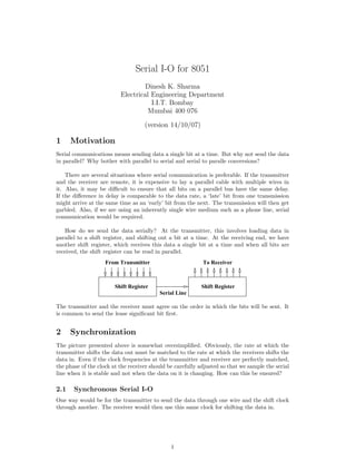
  • 1. Serial I-O for 8051 Dinesh K. Sharma Electrical Engineering Department I.I.T. Bombay Mumbai 400 076 (version 14/10/07) 1 Motivation Serial communications means sending data a single bit at a time. But why not send the data in parallel? Why bother with parallel to serial and serial to paralle conversions? There are several situations where serial communication is preferable. If the transmitter and the receiver are remote, it is expensive to lay a parallel cable with multiple wires in it. Also, it may be difficult to ensure that all bits on a parallel bus have the same delay. If the difference in delay is comparable to the data rate, a ‘late’ bit from one transmission might arrive at the same time as an ‘early’ bit from the next. The transmission will then get garbled. Also, if we are using an inherently single wire medium such as a phone line, serial communication would be required. How do we send the data serially? At the transmitter, this involves loading data in parallel to a shift register, and shifting out a bit at a time. At the receiving end, we have another shift register, which receives this data a single bit at a time and when all bits are received, the shift register can be read in parallel. Shift Register Shift Register To ReceiverFrom Transmitter Serial Line The transmitter and the receiver must agree on the order in which the bits will be sent. It is common to send the lease significant bit first. 2 Synchronization The picture presented above is somewhat oversimplified. Obviously, the rate at which the transmitter shifts the data out must be matched to the rate at which the receivers shifts the data in. Even if the clock frequencies at the transmitter and receiver are perfectly matched, the phase of the clock at the receiver should be carefully adjusted so that we sample the serial line when it is stable and not when the data on it is changing. How can this be ensured? 2.1 Synchronous Serial I-O One way would be for the transmitter to send the data through one wire and the shift clock through another. The receiver would then use this same clock for shifting the data in. 1
  • 2. Shift Register Shift Register To ReceiverFrom Transmitter Data Shift Clock If the transmitter places data on the positive edge and the receiver samples the data at the negative edge, the data will be stable at the sampling instant. However, this doubles the wire cost. Therefore, this solution is practical only if the transmitter and the receiver are located close to each other. This way of sending serial data is called synchronous serial IO. It is useful for sending data over short distances. The advantage of this method is that it can achieve very high data rates. The 8051 provides support for this method through one of the modes defined for its serial IO (mode 0). 2.2 Asynchronous Serial I-O If the transmitter and the receiver are physically remote, they must use independent shift clock generators, set nominally to the same frequency. In this case, their clock frequencies will invariable have a small but non-zero mismatch. Unfortunately, this means that with time, the sampling time will drift further and further away from the ideal sampling instant. When the sampling time has shifted by more than a half period, the receiver might sample the wrong bit on the serial line, leading to errors. Obviously some means of synchronization must be provided to avoid this and to ensure reliable transfer of data. Since we don’t want to add any more wires, it is clear that the wire carrying data is the one which must carry the extra information required for synchronization. This involves sending extra bits on the wire along with the data. The data bits along with the added bits constitute a frame To synchronize two clocks, we need to create an edge. Serial transmission often uses ‘non return to zero’ or NRZ encoding to minimize noise and power dissipation. If successive bits are identical, no edge may be generated by the data itself. To ensure that an edge occurs at the start of every frame, we add a bit before and a bit after the useful data. These bits are chosen to be different in value, thus ensuring that each frame starts with a value different from the one with which the previous one ended. These are called start and stop bits. It is common to use a ‘1’ for a stop bit and a ‘0’ for a start bit. Then each frame begins with a negative edge. Start 1 0 0 1 1 0 1 0 Write instants Stop T T T T T T T T Sampling Instants Serial Data T T/2 Each new bit is placed on the serial line after time T. (This is called bit time and the corre- sponding frequency the baud rate). Notice that the first sampling instant is offset from the writing instant by half a bit time. This is to ensure that a bit is sampled in the middle of the bit interval T, where it is stable. After sampling the start bit, each bit is sampled a time T after the previous bit. 2
  • 3. Often a ‘Parity bit’ is also added to the data. The transmitter and the receiver agree to use either even or odd parity. The parity bit is chosen by the transmitter to be a ‘0’ or a ‘1’ so that the total number of bits in a frame is always even (or always odd). The receiver counts the number of ‘1’s and ensures that the count is ‘even’ (or odd) as previously agreed with the transmitter. If it is not, it can signal an error and the software can take appropriate action (such as a request for re-transmission). The use of parity bit is optional. The receiver now knows that a frame will always begin with an edge. It uses a locally generated clock for synchronization and timing. Because of small mismatches in transmit and receive clocks, the ‘start of frame’ edge on the serial data may not coincide with an edge on the locally generated clock. We take the next edge of the local clock as the effective start of frame. The error in timing due to this could be as much as a whole cycle of the local clock. Obviously, the local clock should not operate at the data rate - a timing error of 1 bit time will then shift the data by 1 bit! Therefore, the locally generated clock operates at a frequency much higher than the bit rate. This high frequency clock is divided down to get the shift clock. For example, the locally generated clock might operate at 32 times the shift clock. A 5 bit counter will be used to divide the local clock. The worst case error in timing will now be one cycle of the locally generated clock. Since it is running at a frequency much higher than the shift clock, this error will be small. start b0 b1 b2 b3 b4 b5 b7 stopb6 (LSB) (MSB) Sampling Instants T T T T T T T T TT/2 Frame Detect 0 1 Time Synchronization occurs at the beginning of each frame. Therefore timing errors do not accumulate from frame to frame. The counter used to divide the local clock is reset when the ‘start of frame’ edge is detected. In the example that we have chosen (internal clock = 32X bit rate), we reset the 5 bit counter when we detect the frame edge. Now, after 16 cycles of the internal clock, (corresponding to time T/2 where T is the interval between bits) the start bit is sampled. If it is not ‘0’, a ‘framing error has occurred and should be handled in software – say by a request to re-transmit. If the start bit is correctly sampled, data bits will be sampled every 32 counts, till all data bits have been sampled. (This might be 8 bits if no parity bit is appended and 9 bits if parity bit is used). The next bit must be the stop bit (normally a ‘1’). If it is not the correct value, a frame error has occurred and must be handled appropriately. If the stop bit is correctly received, we accept the data and wait for the next ‘start of frame’. Notice that this scheme will work equally well, if additional delay is inserted between the end of one frame and the beginning of the next. After the last bit has been sampled, no further timing needs to be performed. The serial line idles at the stop bit (normally ‘1’). The counter is reset to zero whenever the next frame edge is detected. Therefore it does not matter how much time elapses between the end of a frame and the beginning of the next. 2.3 Serial IO protocol Before serial communications can be carried out, the transmitter and the receiver must agree on a number of parameters. • Whether synchronous or asynchronous serial communication will be used. 3
  • 4. • At what rate will the bits be sent. • How many bits will be sent at a time (frame size). • Whether parity will be used and if so, which kind of parity (even or odd) will be used. • Whether simultaneous transmission and reception (duplex) will be possible or only one of these will be carried out at a time (simplex). These parameters constitute the serial protocol. A circuit which implements asynchronous serial communication protocol is known as a Universal Asynchronous Receiver Transmitter (UART). If it can also carry out synchronous serial communication, it is called a USART (Universal Synchronous Asynchronous Receiver Transmitter). Microprocessors often use ded- icated chips like the Intel 8251 USART for implementing serial communication. The 8051 has a built in USART. 3 Implementation of Serial Port in 8051 The 8051 architecture is designed to make sending and receiving serial data quite simple. It is capable of duplex communication, that is serial transmission and reception can be carried out simultaneously. Pins of port 3 perform a dual function. P3.0 can also serve as the serial data input (RxD) and P3.1 can serve as the serial data output (TxD) when serial IO has been enabled. The 8051 contains two registers, one for receiving and the other for sending serial data. Both of these respond to the same address (99H) in the special function register area. (The assembler aliases the address 99H to the name Sbuf). The receive register places data on the internal bus when a read is performed from Sbuf (99H), while the transmit register receives the data when a write operation is carried out to this address. TxD RxD Sbuf Sbuf Shift Reg. Internal Data Bus Wr Rd Clock Control The transmit register itself acts as the shift register for outputting serial data through the TxD pin (P3.1). When the data has been shifted out, a flag called TI is set, inviting the processor to write fresh data to Sbuf. The serial data input pin RxD (P3.0) is connected to an independent shift register, whose output is transferred to the receive buffer after a complete frame has been shifted in. A flag (RI) is set at this time to inform the processor that serial data is available for reading at Sbuf. Flags RI and TI are parts of a bit addressable register SCON, which resides at address 98H in the special function register area. SCON is used for configuring serial communication. 3.1 Configuring the Serial Port Configuration of the serial port involves choosing the mode of communication, deciding rate of sending data and managing the parity bit etc. Much of this work is done by the special function register SCON at byte address 98H in the SFR area. SCON is bit addressable. SCON register at BYTE address 98H Bit No. 7 6 5 4 3 2 1 0 Bit Addr 9F 9E 9D 9C 9B 9A 99 98 Bit Name SM0 SM1 SM2 REN TB8 RB8 TI RI 4
  • 5. As described before, two physically distinct registers responding to the byte address 99H are used as transmit and receive buffers during serial IO. In addition to these resources, the most significant bit of the PCON register at address 87H (known as SMOD) is used for doubling the baud rate when set. The upper nibble of SCON configures the operation of the serial IO, while the lower nibble is used for auxiliary data arising per frame during communication. SM0 and SM1 decide the mode of communication. (Note the somewhat non-standard convention of calling the more significant bit SM0 and the less significant bit SM1). SM0 determines if 8bits of data will be sent per frame (SM0=0) or 9 (when SM0=1). 9 bits are used when we want to send a parity bit in addition to 8bit data. 9 bit communication is also used in a special way with SM2 during multicast communication. SM1 determines if fixed or variable baud rate will be used. SM2 is used for multicast transmission and will be explained later. In normal use, it should be kept cleared. REN must be set to enable reception of data on the RxD line. (What would happen if serial reception is permanently enabled?) If we use a parity bit, we need to send and receive 9 bits of data along with the start and stop bits in every frame. Sbuf can hold only 8 bits each in the send and receive buffers. Where can the 9th bit be accommodated? Bits TB8 and RB8 in SCON are used to ac- commodate the 9th bit during transmission and reception respectively. When all bits of a frame have been received serially, the hardware in 8051 sets the flag RI. This is an invitation to the processor to read Sbuf (and if necessary, RB8). Similarly, TI is set when the frame corresponding to the data written to Sbuf (and if necessary, TB8) have been shifted out of the TxD line. This is an invitation to write fresh data to Sbuf if more data needs to be sent out on the serial line. Notice that TI and RI are not automatically cleared and must be cleared by software which reads/writes Sbuf. It is possible to enable a special interrupt called Serial Interrupt. This is triggered by the OR of TI and RI. The interrupt service routine is supposed to examine the flags TI and RI and take appropriate action accordingly. 3.2 Serial IO modes SM0 and SM1 determine the mode of serial IO. Mode 0 This mode corresponds to SM0=0 and SM1=0. This is a Shift Register mode: Data is transmitted as well as received through the RxD pin and the shift clock is supplied through the TxD pin. Since shift clock is supplied separately, there is no need for a start and a stop bit. 8 bits of data are transmitted or received (SM0 = 0) at a fixed rate (SM1 = 0) given by the crystal oscillator frequency divided by 12. Mode 1 This mode corresponds to SM0 = 0 and SM1 = 1, and is a duplex UART mode. Data is sent through the TxD pin and received through the RxD pin. A 10 bit frame frame containing 8 bit data (SM0=0), a start bit (=0) and a stop bit (=1) are used. The rate of sending and receiving data is set by the overflow rate of timer T1 (SM1 = 1 implies variable data rate). Details of how T1 is used will be discussed later. The data rate can be doubled by setting the most significant bit of the special function register PCON at address 87H. This bit is called SMOD. Notice that PCON is not bit addressable and masking must be used to set or clear this bit without disturbing the rest of PCON, which controls the sleep and idle modes to reduce power dissipation during times of low activity. The stop bit sampled on the serial input line is copied to bit RB8 in SCON in this mode. Mode 2 This mode is set by making SM0 = 1 (11 bit frame containing 9 bits of data, start and stop bit) and SMO = 0 (fixed baud rate). This is an asynchronous mode using a start and stop bit. Serial data is transmitted using the TxD pin and received using the RxD pin. The baud rate is fixed at fosc/64. The baud rate can be doubled to fosc/32 by setting the SMOD bit. 5
  • 6. Mode 3 This mode is set by making SM0 = 1 (11 bit frame containing 9 bits of data, start and stop bit) and SMO = 1 (variable baud rate). This is an asynchronous mode using a start and stop bit (identical to mode 2) except that the baud rate is determined from the overflow rate of timer T1. Serial data is transmitted using the TxD pin and received using the RxD pin. The baud rate in modes 1,2 and 3 can be doubled by setting the bit SMOD (PCON.7). 3.3 Serial I-O using Interrupts To do serial I-O under interrupt control, we need to enable serial interrupts by setting bits 4 (ES) and 7 (EA) of the interrupt enable special function register IE at byte address A8H. This register is bit addressable. (The assembler gives special mnemonics to each bit address.) SFR IE at byte address A8H Bit No. 7 6 5 4 3 2 1 0 Function IE U U SI TF1 Ex1 TF0 Ex0 Bit Addr AF AE AD AC AB AA A9 A8 Bit Name EA - - ES ET1 EX1 ET0 EX0 The most significant bit of the register is a global interrupt enable flag. This bit must be set in order to enable any interrupt. Bit 4 (ES) enables interrupt from the serial interface. Once enabled, the serial interface causes interrupts due to a receive event (RI Flag set) or due to a transmit event (TI Flag set). The receive event occurs when the input buffer of the serial line (Sbuf in) is full and a byte needs to be read from it. The transmit event indicates that a byte has been sent and a new byte can be written to output buffer of the serial line (Sbuf out). When a serial interrupt occurs, control is transferred to address 0023H of the program memory, which is the vector address for serial interrupts. The interrupt handler routine is supposed to be placed here. Since only 8 bytes are available in this region for each handler, it is conventional to place the interrupt service routine elsewhere and to place an ljump in- struction at address 0023H to the handler. As discussed earlier, there are independent interrupt flags for reception and transmission of serial data, called RI and TI in the lower nibble of SCON. RI indicates that a byte has been received and is available for reading in the input buffer. TI indicates that the previous byte has been sent serially and a new byte can be written to the serial port. A serial interrupt occurs if either of these flags is set. (Of course the serial interrupt must be enabled for this to occur). The interrupt service routine should check which of these events caused the interrupt. This can be done by examining the flags. Either or both of these flags might be set, requiring a read from or write to the serial buffer Sbuf (or both). Recall that the input and output buffers are distinct but are located at the same address. A read from this address reads the input buffer while a write to the same address writes to the output buffer. The RI and TI flags are not automatically cleared when an interrupt is serviced. Therefore, the interrupt service routine must clear them before returning. Here is an example handler for serial interrupts: Serial_ISR: PUSH PSW ; Save flags and context JNB RI,output ; If RI not set, check for TI MOV inchar, Sbuf; Save this character CLR RI ; clear receive interrupt flag output: ; Check if output is required JNB TI, done ; If no transmit interrupt, leave MOV Sbuf, outchar; Else send the character CLR TI ; Clear Transmit interrupt flag done: POP PSW ; and flags RETI ; and return 6
  • 7. 3.4 Multicast Serial IO The flag SM2 in SCON is used for multicast communication. When SM2 is set, the receive interrupt flag is not set if the received character does not have the 9th bit set. The way this is used is the following: Several ‘slaves’ are connected in parallel to a single ‘master’. Each slave is given a unique address. We use mode 2 or mode 3, which uses 11 bit frames containing 9 bit data, the start bit and the stop bit. The 9th data bit is not used for parity here. It is used in a special way to enable reception of data only by selected receivers. The way this is accomplished is that initially, all ‘slaves’ have their SM2 bits set. Commands are sent by the master with the 9th bit set. (The master can easily do this by loading a ‘1’ in its ‘TB8’ bit in SCON). Because of this, when commands are sent, all ‘slaves’ receive an interrupt and read the command. To illustrate the procedure with an example, assume that the upper nibble of the com- mand encodes what command it is and the lower nibble contains the address of slave to whom it applies. (Thus, up to 16 slaves can be managed in this example). Let us say that a 0001 in the upper nibble means “become an active listener” while 0010 means “stop listening”. In order to make a slave (with address = 7) the active listener, the master can send 0001 0111 with TB8 set. All slaves receive this command because the 9th bit was set. Now slave 7 finds that its address matches the lower nibble. It clears its SM2 bit. The other slaves, for whom the lower nibble of the command did not match their address, continue to keep this bit set. Data is now sent by the master with the 9th bit (TB8) cleared. The selected slave has its SM2 bit cleared. Therefore, it will receive an interrupt whether the 9th bit is set or not. On the other hand, no interrupt is generated in other slaves (because SM2 bit is set and their RB8 is not). Thus they automatically ignore the data. The selected listener can be de-selected by sending the command 0010 0111 with TB8 set. All slaves receive the command (because RB8 is set). Slave 7 knows that this is a command and not data, because its RB8 is set. Since the lower nibble matches its address, it has to act on this command. The upper nibble is 0010, which means “de-select”. So slave 7 sets its SM2 bit again and now will be interrupted only by commands (which have the 9th bit set) and not by data (when the 9th bit is cleared). 4 Baud rate generation In modes 1 and 3, the baud rate is generated by the overflow rate of timer T1. While T1 can be used in any mode for this purpose, it is convenient to use it in the auto reload mode (timer mode 2). This timer mode uses TH1 to store the auto-reload value and uses TL1 as an 8 bit counter. Once configured, T1 runs continuously and needs no further software effort. Its input is the oscillator frequency divided by 12. (Interrupts are not required and in fact must not be enabled for T1). In this mode, T1 will overflow when TL1 reaches 256. At this time, TL1 will be reloaded automatically with the value stored in TH1. Suppose the value n is loaded in TH1 and fc = crystal frequency. TL1 loads the value n and counts up. It reaches 256 after 256-n cycles. Then it reloads itself with n and starts counting up again. So, TL1 will overflow and reload the value n every (256-n) inputs. The frequency of the input to the counter is fc 12 Therefore the frequency of the output is fc 12(256−n) 7
  • 8. This constitutes the 32X clock for synchronization. Therefore the baud rate is: fc 12×32(256−n) Thus, baud rate = fc 384(256−n) In actual use, we are given the baud rate and must determine n. So n = 256 − fc 386 × baud rate If SMOD bit is set, the internal clock is just 16X the baud rate. In that case, baud rate = fc 192(256 − n) so n = 256 − fc 192 × baud rate Let us illustrate it with an example. A crystal frequency of 11.059 MHz is often used because it gives convenient integral values for n for most standard baud rates. Consider a baud rate of 9600. n = 256 − 11059000 384 × 9600 = 256 − 2.9999 ≃ 256 − 3 = 253 If we back calculate the baud rate with this value of n, baud rate = 11059000 384 × 3 = 9599.2 which is close enough. If we want 19200 baud, n = 256 − 11059000 384 × 19200 = 256 − 1.49997 ≃ 256 − 1.5 In this case we do not get an integral value for n. If we use 256-1 = 255, we get baud rate = 11059000 384 × 1 = 28799.48 and if we use 256-2 = 254, we get baud rate = 11059000 384 × 2 = 14399.74 neither of which is anywhere close to what we want. However, in this case, we can set the SMOD bit (PCON.7). Then, n = 256 − 11059000 192 × 19200 = 256 − 2.9999 ≃ 256 − 3 = 253 This gives a baud rate of baud rate = 11059000 192 × 3 = 19199.62 Which is acceptable. This is about the highest standard baud rate possible with a standard 8051 which is rated to run at clock frequencies up to 12 MHz. 8
  • 9. The lowest baud rate we can get using T1 in 8bit auto reload mode is about 110. A count of 0 will give baud rate = 11059000 384 × 256 = 112.4979 which is marginally acceptable for 110 baud communication. (This is because at such low baud rates, we can afford to be a fair bit away from the middle of the bit time and still not run the risk of sampling the wrong bit). However, if we need even lower baud rates this timer mode will not do. In these cases, we can either operate the microcontroller at a lower crystal frequency, or use a 16 bit timer mode and reload the timer in software with a calculated value every time T1 overflows. Calculation of the count now will require us to include the number of clock cycles needed to respond to the interrupt and then to reload the counter. Fortunately, the use of baud rates below 110 is extremely rare. 5 Putting it all together Here is the list of things we need to do in order to communicate serially. 5.1 Configuration For configuring asynchronous serial communication at a given baud rate to be set by T1: 1. Write the interrupt service routine for serial interrupts. (An example has been provided earlier). Place an ljump to it at the vector address 0023. 2. Set SCON bits to desired values. SCON register at BYTE address 98H Bit No. 7 6 5 4 3 2 1 0 Bit Addr 9F 9E 9D 9C 9B 9A 99 98 Bit Name SM0 SM1 SM2 REN TB8 RB8 TI RI For communication without the parity bit, clear SM0. Set SM0 for communication with parity. Since baud rate is to be decided by T1, set SM1. Clear SM2, as we are not using multicast transmission. We should (eventually) set REN, but it is better to do this as the last step to avoid receiving invalid data before configuration is complete. 3. Configure T1 to provide the desired baud rate. This requires setting appropriate bits in TCON and TMOD registers and loading the appropriate delay value in TH1. TCON register at BYTE address 88H Bit No. 7 6 5 4 3 2 1 0 Bit Name TF1 TR1 TF0 TR0 IE1 IT1 IE0 IT0 Bit Addr 8F 8E 8D 8C 8B 8A 89 88 TMOD register at BYTE address 89H Bit No. 7 6 5 4 3 2 1 0 Timer: T1 T0 Bit Name G1 C/T1 T1M1 T1M0 G0 C/T0 T0M1 T0M0 We need to disable hardware gating for T1 (G1 = 0), use it as a timer (C/T1 = 0), and put it in 8bit auto reload mode (T1M1 = 1, T1M0 = 0). Since TMOD is not bit addressable and we don’t want to disturb T0 settings, we do it by ORing TMOD with #20H and ANDing it with #2FH. We set TR1 in TCON to allow T1 to run. 4. Calculate the value to be loaded in TH1 as described earlier. If we need to double the baud rate to get an integer value for n, set SMOD (PCON.7) by ORing it with #80H. Else, clear it by ANDing it with #7FH. (This is because PCON is not bit addressable). Load TH1 with #n. 9
  • 10. 5. Enable serial interrupts and disable interrupts from T1. This is done by manipulating the specil function register IE. Interrupt Enable Register IE at A8H Bit No. 7 6 5 4 3 2 1 0 Bit Addr AF AE AD AC AB AA A9 A8 Interrupt on IE U U SI TF1 Ex1 TF0 Ex0 Bit Name EA - - ES ET1 EX1 ET0 EX0 We need to set EA (IE.7), ES (IE.4) and clear ET1. IE is bit addressable. 6. Now we are ready: clear RI and TI to remove any stale flags and set REN in SCON to enable serial I-O. 5.2 Using the serial port Once the configuration is done, it is easy to use the port. On a receive interrupt, we just read SBUF and clear RI. On a transmit interrupt, we write the byte to SBUF. If parity is being used, we can just add 0 to the byte in A and copy the parity flag (PSW.0) to TB8 in SCON before writing to SBUF. 10