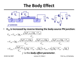
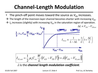
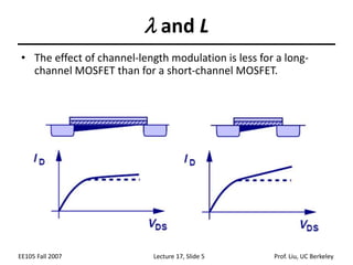
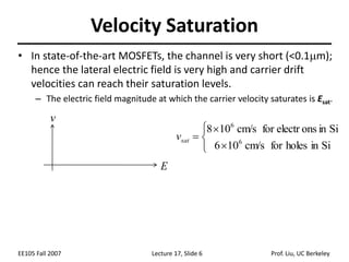
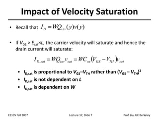
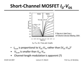
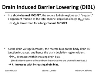
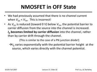
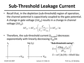
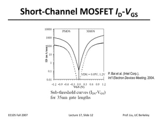
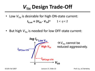
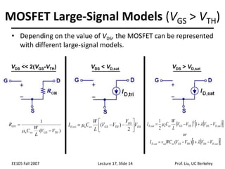
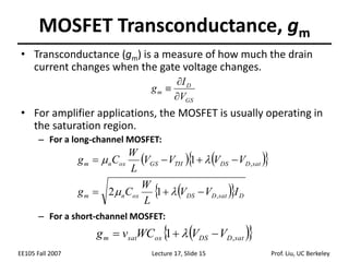
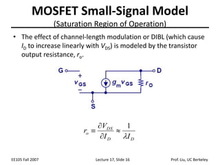
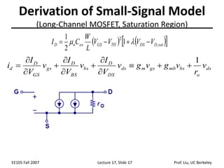
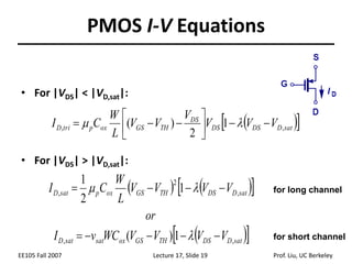
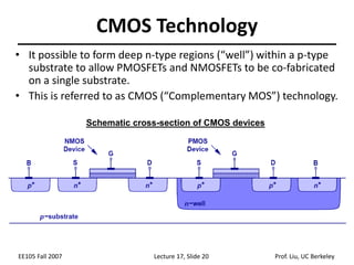
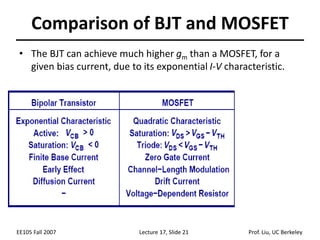
SlideShare a Scribd company logo
EE105 Fall 2007 Lecture 17, Slide 1 Prof. Liu, UC Berkeley
Lecture 17
OUTLINE
• NMOSFET in ON state (cont’d)
– Body effect
– Channel-length modulation
– Velocity saturation
• NMOSFET in OFF state
• MOSFET models
• PMOSFET
Reading: Finish Chapter 6
ANNOUNCEMENTS
• Wed. discussion section moved (again) to 6-7PM in 293 Cory
EE105 Fall 2007 Lecture 17, Slide 2 Prof. Liu, UC Berkeley
The Body Effect
   
B
SB
B
TH
B
SB
B
ox
Si
A
TH
ox
SB
B
Si
A
ox
B
Si
A
ox
B
Si
A
B
FB
ox
SB
B
Si
A
B
FB
TH
V
V
V
C
qN
V
C
V
qN
C
qN
C
qN
V
C
V
qN
V
V
















2
2
2
2
2
)
2
(
2
)
2
(
2
)
2
(
2
2
)
2
(
2
2
0
0 

















• VTH is increased by reverse-biasing the body-source PN junction:
 is the body effect parameter.
EE105 Fall 2007 Lecture 17, Slide 3 Prof. Liu, UC Berkeley
Body Effect Example
 
ox
Si
A
B
SB
B
TH
TH
C
qN
V
V
V





2
where
2
2
0





EE105 Fall 2007 Lecture 17, Slide 4 Prof. Liu, UC Berkeley
Channel-Length Modulation
• The pinch-off point moves toward the source as VDS increases.
 The length of the inversion-layer channel becomes shorter with increasing VDS.
 ID increases (slightly) with increasing VDS in the saturation region of operation.
   
 
sat
D
DS
TH
GS
ox
n
sat
D V
V
V
V
L
W
C
I ,
2
, 1
2
1



 

 is the channel length modulation coefficient.





 





L
L
L
L
L
IDsat 1
1
1
DSsat
DS V
V
L 


EE105 Fall 2007 Lecture 17, Slide 5 Prof. Liu, UC Berkeley
 and L
• The effect of channel-length modulation is less for a long-
channel MOSFET than for a short-channel MOSFET.
EE105 Fall 2007 Lecture 17, Slide 6 Prof. Liu, UC Berkeley
Velocity Saturation
• In state-of-the-art MOSFETs, the channel is very short (<0.1m);
hence the lateral electric field is very high and carrier drift
velocities can reach their saturation levels.
– The electric field magnitude at which the carrier velocity saturates is Esat.






Si
in
holes
for
cm/s
10
6
Si
in
s
on
for electr
cm/s
10
8
6
6
sat
v
v
E
EE105 Fall 2007 Lecture 17, Slide 7 Prof. Liu, UC Berkeley
Impact of Velocity Saturation
• Recall that
• If VDS > Esat×L, the carrier velocity will saturate and hence the
drain current will saturate:
• ID,sat is proportional to VGS–VTH rather than (VGS – VTH)2
• ID,sat is not dependent on L
• ID,sat is dependent on W
)
(
)
( y
v
y
WQ
I inv
D 
  sat
TH
GS
ox
sat
inv
sat
D v
V
V
WC
v
WQ
I 


,
EE105 Fall 2007 Lecture 17, Slide 8 Prof. Liu, UC Berkeley
• ID,sat is proportional to VGS-VTH rather than (VGS-VTH)2
• VD,sat is smaller than VGS-VTH
• Channel-length modulation is apparent (?)
Short-Channel MOSFET ID-VDS
P. Bai et al. (Intel Corp.),
Int’l Electron Devices Meeting, 2004.
EE105 Fall 2007 Lecture 17, Slide 9 Prof. Liu, UC Berkeley
• In a short-channel MOSFET, the source & drain regions each “support”
a significant fraction of the total channel depletion charge Qdep×W×L
 VTH is lower than for a long-channel MOSFET
• As the drain voltage increases, the reverse bias on the body-drain PN
junction increases, and hence the drain depletion region widens.
VTH decreases with increasing drain bias.
(The barrier to carrier diffusion from the source into the channel is reduced.)
 ID increases with increasing drain bias.
Drain Induced Barrier Lowering (DIBL)
EE105 Fall 2007 Lecture 17, Slide 10 Prof. Liu, UC Berkeley
NMOSFET in OFF State
• We had previously assumed that there is no channel current
when VGS < VTH. This is incorrect!
• As VGS is reduced (toward 0 V) below VTH, the potential barrier to
carrier diffusion from the source into the channel is increased.
ID becomes limited by carrier diffusion into the channel, rather
than by carrier drift through the channel.
(This is similar to the case of a PN junction diode!)
ID varies exponentially with the potential barrier height at the
source, which varies directly with the channel potential.
EE105 Fall 2007 Lecture 17, Slide 11 Prof. Liu, UC Berkeley
Sub-Threshold Leakage Current
• Recall that, in the depletion (sub-threshold) region of operation,
the channel potential is capacitively coupled to the gate potential.
A change in gate voltage (VGS) results in a change in channel
voltage (VCS):
• Therefore, the sub-threshold current (ID,subth) decreases
exponentially with linearly decreasing VGS/m
m
V
C
C
C
V
V GS
dep
ox
ox
GS
CS /















log (ID)
VGS
ID
VGS
mV/dec
60
)
10
(
ln
)
(log
1
10












T
GS
DS
mV
S
dV
I
d
S
“Sub-threshold swing”:
EE105 Fall 2007 Lecture 17, Slide 12 Prof. Liu, UC Berkeley
Short-Channel MOSFET ID-VGS
P. Bai et al. (Intel Corp.),
Int’l Electron Devices Meeting, 2004.
EE105 Fall 2007 Lecture 17, Slide 13 Prof. Liu, UC Berkeley
VTH Design Trade-Off
• Low VTH is desirable for high ON-state current:
ID,sat  (VDD - VTH) 1 <  < 2
• But high VTH is needed for low OFF-state current:
VTH cannot be
reduced aggressively.
Low VTH
High VTH
IOFF,high VTH
IOFF,low VTH
VGS
log ID
0
EE105 Fall 2007 Lecture 17, Slide 14 Prof. Liu, UC Berkeley
MOSFET Large-Signal Models (VGS > VTH)
• Depending on the value of VDS, the MOSFET can be represented
with different large-signal models.
   
 
 
 
sat
D
DS
TH
GS
ox
sat
sat
D
sat
D
DS
TH
GS
ox
n
sat
D
V
V
V
V
WC
v
I
or
V
V
V
V
L
W
C
I
,
,
,
2
,
1
)
(
1
2
1











VDS << 2(VGS-VTH)
)
(
1
TH
GS
ox
n
ON
V
V
L
W
C
R



VDS < VD,sat
DS
DS
TH
GS
ox
n
tri
D V
V
V
V
L
W
C
I 








2
)
(
, 
VDS > VD,sat
EE105 Fall 2007 Lecture 17, Slide 15 Prof. Liu, UC Berkeley
MOSFET Transconductance, gm
• Transconductance (gm) is a measure of how much the drain
current changes when the gate voltage changes.
• For amplifier applications, the MOSFET is usually operating in
the saturation region.
– For a long-channel MOSFET:
– For a short-channel MOSFET:
   
 
 
  D
sat
D
DS
ox
n
m
sat
D
DS
TH
GS
ox
n
m
I
V
V
L
W
C
g
V
V
V
V
L
W
C
g
,
,
1
2
1











GS
D
m
V
I
g



 
 
sat
D
DS
ox
sat
m V
V
WC
v
g ,
1 

 
EE105 Fall 2007 Lecture 17, Slide 16 Prof. Liu, UC Berkeley
MOSFET Small-Signal Model
(Saturation Region of Operation)
D
D
DS
o
I
I
V
r

1




• The effect of channel-length modulation or DIBL (which cause
ID to increase linearly with VDS) is modeled by the transistor
output resistance, ro.
EE105 Fall 2007 Lecture 17, Slide 17 Prof. Liu, UC Berkeley
Derivation of Small-Signal Model
(Long-Channel MOSFET, Saturation Region)
ds
o
bs
mb
gs
m
ds
DS
D
bs
BS
D
gs
GS
D
d v
r
v
g
v
g
v
V
I
v
V
I
v
V
I
i
1












   
 
sat
D
DS
TH
GS
ox
n
D V
V
V
V
L
W
C
I ,
2
1
2
1



 

EE105 Fall 2007 Lecture 17, Slide 18 Prof. Liu, UC Berkeley
PMOS Transistor
• A p-channel MOSFET behaves similarly to an n-channel
MOSFET, except the polarities for ID and VGS are reversed.
• The small-signal model for a PMOSFET is the same as that for
an NMOSFET.
– The values of gm and ro will be different for a PMOSFET vs. an NMOSFET,
since mobility & saturation velocity are different for holes vs. electrons.
Circuit symbol
Schematic cross-section
EE105 Fall 2007 Lecture 17, Slide 19 Prof. Liu, UC Berkeley
PMOS I-V Equations
• For |VDS| < |VD,sat|:
• For |VDS| > |VD,sat|:
 
 
sat
D
DS
DS
DS
TH
GS
ox
p
tri
D V
V
V
V
V
V
L
W
C
I ,
, 1
2
)
( 









 

   
 
 
 
sat
D
DS
TH
GS
ox
sat
sat
D
sat
D
DS
TH
GS
ox
p
sat
D
V
V
V
V
WC
v
I
or
V
V
V
V
L
W
C
I
,
,
,
2
,
1
)
(
1
2
1











 for long channel
for short channel
EE105 Fall 2007 Lecture 17, Slide 20 Prof. Liu, UC Berkeley
CMOS Technology
• It possible to form deep n-type regions (“well”) within a p-type
substrate to allow PMOSFETs and NMOSFETs to be co-fabricated
on a single substrate.
• This is referred to as CMOS (“Complementary MOS”) technology.
Schematic cross-section of CMOS devices
EE105 Fall 2007 Lecture 17, Slide 21 Prof. Liu, UC Berkeley
Comparison of BJT and MOSFET
• The BJT can achieve much higher gm than a MOSFET, for a
given bias current, due to its exponential I-V characteristic.

More Related Content

Similar to 5172197.ppt

Very Large Scale Integration -VLSI
Very Large Scale Integration -VLSIVery Large Scale Integration -VLSI
Very Large Scale Integration -VLSI
PRABHAHARAN429
 
Lecture21-BJT ExamplesAnd Pspice based sSim.pdf
Lecture21-BJT ExamplesAnd Pspice based sSim.pdfLecture21-BJT ExamplesAnd Pspice based sSim.pdf
Lecture21-BJT ExamplesAnd Pspice based sSim.pdf
Balraj Singh
 
Simulation Studies of ZnO Nanowire Field-Effect Transistor
Simulation Studies of ZnO Nanowire Field-Effect TransistorSimulation Studies of ZnO Nanowire Field-Effect Transistor
Simulation Studies of ZnO Nanowire Field-Effect Transistor
noelds
 

Similar to 5172197.ppt (20)

CNTFET
CNTFETCNTFET
CNTFET
 
Short channel modified
Short channel modifiedShort channel modified
Short channel modified
 
Power and Delay in a FET.pdf
Power and Delay in a FET.pdfPower and Delay in a FET.pdf
Power and Delay in a FET.pdf
 
small geometry effect and working of solar cell
small geometry effect and working of solar cellsmall geometry effect and working of solar cell
small geometry effect and working of solar cell
 
Analog_chap_02.ppt
Analog_chap_02.pptAnalog_chap_02.ppt
Analog_chap_02.ppt
 
Ch7 lecture slides Chenming Hu Device for IC
Ch7 lecture slides Chenming Hu Device for ICCh7 lecture slides Chenming Hu Device for IC
Ch7 lecture slides Chenming Hu Device for IC
 
Metal Oxide Semiconductor Field Effect Transistors
Metal Oxide Semiconductor Field Effect TransistorsMetal Oxide Semiconductor Field Effect Transistors
Metal Oxide Semiconductor Field Effect Transistors
 
Very Large Scale Integration -VLSI
Very Large Scale Integration -VLSIVery Large Scale Integration -VLSI
Very Large Scale Integration -VLSI
 
Lecture21-BJT ExamplesAnd Pspice based sSim.pdf
Lecture21-BJT ExamplesAnd Pspice based sSim.pdfLecture21-BJT ExamplesAnd Pspice based sSim.pdf
Lecture21-BJT ExamplesAnd Pspice based sSim.pdf
 
Negative Capacitance FET
Negative Capacitance FETNegative Capacitance FET
Negative Capacitance FET
 
Simulation Studies of ZnO Nanowire Field-Effect Transistor
Simulation Studies of ZnO Nanowire Field-Effect TransistorSimulation Studies of ZnO Nanowire Field-Effect Transistor
Simulation Studies of ZnO Nanowire Field-Effect Transistor
 
Rec101 unit ii (part 3) field effect transistor
Rec101 unit ii (part 3) field effect transistorRec101 unit ii (part 3) field effect transistor
Rec101 unit ii (part 3) field effect transistor
 
Electronics 1 : Chapter # 08 : Field effect transistor
Electronics 1 : Chapter # 08 : Field effect transistorElectronics 1 : Chapter # 08 : Field effect transistor
Electronics 1 : Chapter # 08 : Field effect transistor
 
Effects of Scaling on MOS Device Performance
Effects of Scaling on MOS Device PerformanceEffects of Scaling on MOS Device Performance
Effects of Scaling on MOS Device Performance
 
Power Converter Systems .ppt
Power Converter Systems .pptPower Converter Systems .ppt
Power Converter Systems .ppt
 
Lecture8
Lecture8Lecture8
Lecture8
 
Variable Body Biasing (VBB) based VLSI Design Approach to Reduce Static Power
Variable Body Biasing (VBB) based VLSI Design Approach to Reduce Static Power Variable Body Biasing (VBB) based VLSI Design Approach to Reduce Static Power
Variable Body Biasing (VBB) based VLSI Design Approach to Reduce Static Power
 
Structural and Electrical Analysis of Various MOSFET Designs
Structural and Electrical Analysis of Various MOSFET DesignsStructural and Electrical Analysis of Various MOSFET Designs
Structural and Electrical Analysis of Various MOSFET Designs
 
comparator.pptx
comparator.pptxcomparator.pptx
comparator.pptx
 
Metal Insulator Semiconductor devices
Metal Insulator Semiconductor devicesMetal Insulator Semiconductor devices
Metal Insulator Semiconductor devices
 

More from kavita417551 (6)

9402094.ppt
9402094.ppt9402094.ppt
9402094.ppt
 
5006278.ppt
5006278.ppt5006278.ppt
5006278.ppt
 
5378086.ppt
5378086.ppt5378086.ppt
5378086.ppt
 
9077262.ppt
9077262.ppt9077262.ppt
9077262.ppt
 
11136442.ppt
11136442.ppt11136442.ppt
11136442.ppt
 
Lec-2.pdf
Lec-2.pdfLec-2.pdf
Lec-2.pdf
 

Recently uploaded

CFD Simulation of By-pass Flow in a HRSG module by R&R Consult.pptx
CFD Simulation of By-pass Flow in a HRSG module by R&R Consult.pptxCFD Simulation of By-pass Flow in a HRSG module by R&R Consult.pptx
CFD Simulation of By-pass Flow in a HRSG module by R&R Consult.pptx
R&R Consult
 
Digital Signal Processing Lecture notes n.pdf
Digital Signal Processing Lecture notes n.pdfDigital Signal Processing Lecture notes n.pdf
Digital Signal Processing Lecture notes n.pdf
AbrahamGadissa
 
Automobile Management System Project Report.pdf
Automobile Management System Project Report.pdfAutomobile Management System Project Report.pdf
Automobile Management System Project Report.pdf
Kamal Acharya
 
Hall booking system project report .pdf
Hall booking system project report  .pdfHall booking system project report  .pdf
Hall booking system project report .pdf
Kamal Acharya
 

Recently uploaded (20)

Arduino based vehicle speed tracker project
Arduino based vehicle speed tracker projectArduino based vehicle speed tracker project
Arduino based vehicle speed tracker project
 
KIT-601 Lecture Notes-UNIT-5.pdf Frame Works and Visualization
KIT-601 Lecture Notes-UNIT-5.pdf Frame Works and VisualizationKIT-601 Lecture Notes-UNIT-5.pdf Frame Works and Visualization
KIT-601 Lecture Notes-UNIT-5.pdf Frame Works and Visualization
 
ASME IX(9) 2007 Full Version .pdf
ASME IX(9)  2007 Full Version       .pdfASME IX(9)  2007 Full Version       .pdf
ASME IX(9) 2007 Full Version .pdf
 
ONLINE CAR SERVICING SYSTEM PROJECT REPORT.pdf
ONLINE CAR SERVICING SYSTEM PROJECT REPORT.pdfONLINE CAR SERVICING SYSTEM PROJECT REPORT.pdf
ONLINE CAR SERVICING SYSTEM PROJECT REPORT.pdf
 
CFD Simulation of By-pass Flow in a HRSG module by R&R Consult.pptx
CFD Simulation of By-pass Flow in a HRSG module by R&R Consult.pptxCFD Simulation of By-pass Flow in a HRSG module by R&R Consult.pptx
CFD Simulation of By-pass Flow in a HRSG module by R&R Consult.pptx
 
NO1 Pandit Black Magic Removal in Uk kala jadu Specialist kala jadu for Love ...
NO1 Pandit Black Magic Removal in Uk kala jadu Specialist kala jadu for Love ...NO1 Pandit Black Magic Removal in Uk kala jadu Specialist kala jadu for Love ...
NO1 Pandit Black Magic Removal in Uk kala jadu Specialist kala jadu for Love ...
 
Furniture showroom management system project.pdf
Furniture showroom management system project.pdfFurniture showroom management system project.pdf
Furniture showroom management system project.pdf
 
Democratizing Fuzzing at Scale by Abhishek Arya
Democratizing Fuzzing at Scale by Abhishek AryaDemocratizing Fuzzing at Scale by Abhishek Arya
Democratizing Fuzzing at Scale by Abhishek Arya
 
Digital Signal Processing Lecture notes n.pdf
Digital Signal Processing Lecture notes n.pdfDigital Signal Processing Lecture notes n.pdf
Digital Signal Processing Lecture notes n.pdf
 
A case study of cinema management system project report..pdf
A case study of cinema management system project report..pdfA case study of cinema management system project report..pdf
A case study of cinema management system project report..pdf
 
NO1 Pandit Amil Baba In Bahawalpur, Sargodha, Sialkot, Sheikhupura, Rahim Yar...
NO1 Pandit Amil Baba In Bahawalpur, Sargodha, Sialkot, Sheikhupura, Rahim Yar...NO1 Pandit Amil Baba In Bahawalpur, Sargodha, Sialkot, Sheikhupura, Rahim Yar...
NO1 Pandit Amil Baba In Bahawalpur, Sargodha, Sialkot, Sheikhupura, Rahim Yar...
 
Automobile Management System Project Report.pdf
Automobile Management System Project Report.pdfAutomobile Management System Project Report.pdf
Automobile Management System Project Report.pdf
 
HYDROPOWER - Hydroelectric power generation
HYDROPOWER - Hydroelectric power generationHYDROPOWER - Hydroelectric power generation
HYDROPOWER - Hydroelectric power generation
 
ENERGY STORAGE DEVICES INTRODUCTION UNIT-I
ENERGY STORAGE DEVICES  INTRODUCTION UNIT-IENERGY STORAGE DEVICES  INTRODUCTION UNIT-I
ENERGY STORAGE DEVICES INTRODUCTION UNIT-I
 
Introduction to Casting Processes in Manufacturing
Introduction to Casting Processes in ManufacturingIntroduction to Casting Processes in Manufacturing
Introduction to Casting Processes in Manufacturing
 
Hall booking system project report .pdf
Hall booking system project report  .pdfHall booking system project report  .pdf
Hall booking system project report .pdf
 
Construction method of steel structure space frame .pptx
Construction method of steel structure space frame .pptxConstruction method of steel structure space frame .pptx
Construction method of steel structure space frame .pptx
 
shape functions of 1D and 2 D rectangular elements.pptx
shape functions of 1D and 2 D rectangular elements.pptxshape functions of 1D and 2 D rectangular elements.pptx
shape functions of 1D and 2 D rectangular elements.pptx
 
İTÜ CAD and Reverse Engineering Workshop
İTÜ CAD and Reverse Engineering WorkshopİTÜ CAD and Reverse Engineering Workshop
İTÜ CAD and Reverse Engineering Workshop
 
Introduction to Machine Learning Unit-4 Notes for II-II Mechanical Engineering
Introduction to Machine Learning Unit-4 Notes for II-II Mechanical EngineeringIntroduction to Machine Learning Unit-4 Notes for II-II Mechanical Engineering
Introduction to Machine Learning Unit-4 Notes for II-II Mechanical Engineering
 

5172197.ppt

  • 1. EE105 Fall 2007 Lecture 17, Slide 1 Prof. Liu, UC Berkeley Lecture 17 OUTLINE • NMOSFET in ON state (cont’d) – Body effect – Channel-length modulation – Velocity saturation • NMOSFET in OFF state • MOSFET models • PMOSFET Reading: Finish Chapter 6 ANNOUNCEMENTS • Wed. discussion section moved (again) to 6-7PM in 293 Cory
  • 2. EE105 Fall 2007 Lecture 17, Slide 2 Prof. Liu, UC Berkeley The Body Effect     B SB B TH B SB B ox Si A TH ox SB B Si A ox B Si A ox B Si A B FB ox SB B Si A B FB TH V V V C qN V C V qN C qN C qN V C V qN V V                 2 2 2 2 2 ) 2 ( 2 ) 2 ( 2 ) 2 ( 2 2 ) 2 ( 2 2 0 0                   • VTH is increased by reverse-biasing the body-source PN junction:  is the body effect parameter.
  • 3. EE105 Fall 2007 Lecture 17, Slide 3 Prof. Liu, UC Berkeley Body Effect Example   ox Si A B SB B TH TH C qN V V V      2 where 2 2 0     
  • 4. EE105 Fall 2007 Lecture 17, Slide 4 Prof. Liu, UC Berkeley Channel-Length Modulation • The pinch-off point moves toward the source as VDS increases.  The length of the inversion-layer channel becomes shorter with increasing VDS.  ID increases (slightly) with increasing VDS in the saturation region of operation.       sat D DS TH GS ox n sat D V V V V L W C I , 2 , 1 2 1        is the channel length modulation coefficient.             L L L L L IDsat 1 1 1 DSsat DS V V L   
  • 5. EE105 Fall 2007 Lecture 17, Slide 5 Prof. Liu, UC Berkeley  and L • The effect of channel-length modulation is less for a long- channel MOSFET than for a short-channel MOSFET.
  • 6. EE105 Fall 2007 Lecture 17, Slide 6 Prof. Liu, UC Berkeley Velocity Saturation • In state-of-the-art MOSFETs, the channel is very short (<0.1m); hence the lateral electric field is very high and carrier drift velocities can reach their saturation levels. – The electric field magnitude at which the carrier velocity saturates is Esat.       Si in holes for cm/s 10 6 Si in s on for electr cm/s 10 8 6 6 sat v v E
  • 7. EE105 Fall 2007 Lecture 17, Slide 7 Prof. Liu, UC Berkeley Impact of Velocity Saturation • Recall that • If VDS > Esat×L, the carrier velocity will saturate and hence the drain current will saturate: • ID,sat is proportional to VGS–VTH rather than (VGS – VTH)2 • ID,sat is not dependent on L • ID,sat is dependent on W ) ( ) ( y v y WQ I inv D    sat TH GS ox sat inv sat D v V V WC v WQ I    ,
  • 8. EE105 Fall 2007 Lecture 17, Slide 8 Prof. Liu, UC Berkeley • ID,sat is proportional to VGS-VTH rather than (VGS-VTH)2 • VD,sat is smaller than VGS-VTH • Channel-length modulation is apparent (?) Short-Channel MOSFET ID-VDS P. Bai et al. (Intel Corp.), Int’l Electron Devices Meeting, 2004.
  • 9. EE105 Fall 2007 Lecture 17, Slide 9 Prof. Liu, UC Berkeley • In a short-channel MOSFET, the source & drain regions each “support” a significant fraction of the total channel depletion charge Qdep×W×L  VTH is lower than for a long-channel MOSFET • As the drain voltage increases, the reverse bias on the body-drain PN junction increases, and hence the drain depletion region widens. VTH decreases with increasing drain bias. (The barrier to carrier diffusion from the source into the channel is reduced.)  ID increases with increasing drain bias. Drain Induced Barrier Lowering (DIBL)
  • 10. EE105 Fall 2007 Lecture 17, Slide 10 Prof. Liu, UC Berkeley NMOSFET in OFF State • We had previously assumed that there is no channel current when VGS < VTH. This is incorrect! • As VGS is reduced (toward 0 V) below VTH, the potential barrier to carrier diffusion from the source into the channel is increased. ID becomes limited by carrier diffusion into the channel, rather than by carrier drift through the channel. (This is similar to the case of a PN junction diode!) ID varies exponentially with the potential barrier height at the source, which varies directly with the channel potential.
  • 11. EE105 Fall 2007 Lecture 17, Slide 11 Prof. Liu, UC Berkeley Sub-Threshold Leakage Current • Recall that, in the depletion (sub-threshold) region of operation, the channel potential is capacitively coupled to the gate potential. A change in gate voltage (VGS) results in a change in channel voltage (VCS): • Therefore, the sub-threshold current (ID,subth) decreases exponentially with linearly decreasing VGS/m m V C C C V V GS dep ox ox GS CS /                log (ID) VGS ID VGS mV/dec 60 ) 10 ( ln ) (log 1 10             T GS DS mV S dV I d S “Sub-threshold swing”:
  • 12. EE105 Fall 2007 Lecture 17, Slide 12 Prof. Liu, UC Berkeley Short-Channel MOSFET ID-VGS P. Bai et al. (Intel Corp.), Int’l Electron Devices Meeting, 2004.
  • 13. EE105 Fall 2007 Lecture 17, Slide 13 Prof. Liu, UC Berkeley VTH Design Trade-Off • Low VTH is desirable for high ON-state current: ID,sat  (VDD - VTH) 1 <  < 2 • But high VTH is needed for low OFF-state current: VTH cannot be reduced aggressively. Low VTH High VTH IOFF,high VTH IOFF,low VTH VGS log ID 0
  • 14. EE105 Fall 2007 Lecture 17, Slide 14 Prof. Liu, UC Berkeley MOSFET Large-Signal Models (VGS > VTH) • Depending on the value of VDS, the MOSFET can be represented with different large-signal models.           sat D DS TH GS ox sat sat D sat D DS TH GS ox n sat D V V V V WC v I or V V V V L W C I , , , 2 , 1 ) ( 1 2 1            VDS << 2(VGS-VTH) ) ( 1 TH GS ox n ON V V L W C R    VDS < VD,sat DS DS TH GS ox n tri D V V V V L W C I          2 ) ( ,  VDS > VD,sat
  • 15. EE105 Fall 2007 Lecture 17, Slide 15 Prof. Liu, UC Berkeley MOSFET Transconductance, gm • Transconductance (gm) is a measure of how much the drain current changes when the gate voltage changes. • For amplifier applications, the MOSFET is usually operating in the saturation region. – For a long-channel MOSFET: – For a short-channel MOSFET:           D sat D DS ox n m sat D DS TH GS ox n m I V V L W C g V V V V L W C g , , 1 2 1            GS D m V I g        sat D DS ox sat m V V WC v g , 1    
  • 16. EE105 Fall 2007 Lecture 17, Slide 16 Prof. Liu, UC Berkeley MOSFET Small-Signal Model (Saturation Region of Operation) D D DS o I I V r  1     • The effect of channel-length modulation or DIBL (which cause ID to increase linearly with VDS) is modeled by the transistor output resistance, ro.
  • 17. EE105 Fall 2007 Lecture 17, Slide 17 Prof. Liu, UC Berkeley Derivation of Small-Signal Model (Long-Channel MOSFET, Saturation Region) ds o bs mb gs m ds DS D bs BS D gs GS D d v r v g v g v V I v V I v V I i 1                   sat D DS TH GS ox n D V V V V L W C I , 2 1 2 1      
  • 18. EE105 Fall 2007 Lecture 17, Slide 18 Prof. Liu, UC Berkeley PMOS Transistor • A p-channel MOSFET behaves similarly to an n-channel MOSFET, except the polarities for ID and VGS are reversed. • The small-signal model for a PMOSFET is the same as that for an NMOSFET. – The values of gm and ro will be different for a PMOSFET vs. an NMOSFET, since mobility & saturation velocity are different for holes vs. electrons. Circuit symbol Schematic cross-section
  • 19. EE105 Fall 2007 Lecture 17, Slide 19 Prof. Liu, UC Berkeley PMOS I-V Equations • For |VDS| < |VD,sat|: • For |VDS| > |VD,sat|:     sat D DS DS DS TH GS ox p tri D V V V V V V L W C I , , 1 2 ) (                        sat D DS TH GS ox sat sat D sat D DS TH GS ox p sat D V V V V WC v I or V V V V L W C I , , , 2 , 1 ) ( 1 2 1             for long channel for short channel
  • 20. EE105 Fall 2007 Lecture 17, Slide 20 Prof. Liu, UC Berkeley CMOS Technology • It possible to form deep n-type regions (“well”) within a p-type substrate to allow PMOSFETs and NMOSFETs to be co-fabricated on a single substrate. • This is referred to as CMOS (“Complementary MOS”) technology. Schematic cross-section of CMOS devices
  • 21. EE105 Fall 2007 Lecture 17, Slide 21 Prof. Liu, UC Berkeley Comparison of BJT and MOSFET • The BJT can achieve much higher gm than a MOSFET, for a given bias current, due to its exponential I-V characteristic.