
Recommended
Recommended
More Related Content
What's hot
What's hot (20)
Similar to лекция 3 дефекты в полупроводниках ga n alsb
Similar to лекция 3 дефекты в полупроводниках ga n alsb (20)
More from Sergey Sozykin
Recently uploaded
Recently uploaded (20)
лекция 3 дефекты в полупроводниках ga n alsb
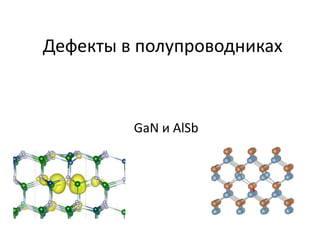
- 1. Дефекты в полупроводниках GaN и AlSb
- 2. Possible trap locations AlGaN Egap=4.2 eV 1 1. Thermally activated to AlGaN Ec 3 2. Tunneling to Gate 2 3. Tunneling to Channel 4. Thermally activated tunneling to Channel 4 GaN Egap=3.4 eV 2’
- 3. Hydrogenated Antisite NH3 Egain = 2.35 eV Exothermic process growth NGaH3 : NEGATIVE FORMATION ENERGY
- 4. Defect Complex VGa-ON E f Dq H x Etot Dq H x bulk Etot ni i q EF Ev V qocc Eshift , i mGa + m N = mGaN bulk m N = m NH - 3 2 m H gas gas 3 2 CBM(GaN) mO = 1 2 m gas O 2
- 5. ~ 0.5 eV
- 6. Results of calculations “0” “-3” C.-H. Lin et. al., Appl. Phys. Lett. (2009) Y. S. Puzyrev, et al., Appl. Phys. Lett. 96, 053505 (2010).
- 7. Candidate defect: hydrogenated Ga vacancy Coulomb Scatterer Neutral defect Transconductance degradation “0” “-3” Remove H Hydrogenated Ga vacancy Yellow Luminescence
- 8. Electrical stress-induced degradation (Process Splits; Critical Experiments) MBE-grown devices (passivated) Electrical stress : VG = −4 V VD = 20 V T = 300 K Positive shift in Ga-rich, N-rich Shift in Vpinch-off is permanent. – acceptors created, or donors removed Negative shift in NH3-rich T. Roy, et al., Appl. Phys. Lett. – donors created or acceptors removed 96, 133503 (2010).
- 9. Source of degradation: hydrogenation of Ga-vacancies • Hot electrons sequentially remove hydrogens from Ga-vacancies • Different charge states “0” Al0.3Ga0.7N “-3” “-2” “-3” “-1” “0” EF during stress T. Roy, et al., Appl. Phys. Lett. 96, 133503 (2010).
- 10. Possible trap locations AlGaN 1 1. Thermally activated to AlGaN Ec 3 2. Tunneling to Gate 2 3. Tunneling to Channel 4. Thermally activated tunneling to Channel 4 GaN 2’
- 11. DFT calculation of Defect Candidates Low formation energies Vacancy complexes with impurities,- O and H Oxygen complexes • VGa-ON • VGa-ON-O Hydrogen Complexes • VGa-VN-H • VGa-VN-H2
- 12. Defect Candidates Oxygen-Hydrogen Complexes • VGa-ON-H • VGa-ON-H2 For example: extended electron state for level ~0.7 eV below CBM of [VGa-ON-H]-2
- 13. Defect Complex VGa-VN-H [VGa-VN-H]-1 CBM(GaN) Localized state ~1.eV below AlGaN CBM
- 14. Thermodynamic Levels ON CBM(GaN) LDA – (0/-1) trap level in conduction band?
- 15. Defect Complex VGa-ON LDA state for [VGa-ON-H]-2 is delocalized CBM(GaN) LDA – (-1/-2) charge transition level in conduction band?
- 16. Defect Complex VGa-ON-H Hybrid Functional calculation Egap = 4.7 V LDA state for [VGa-ON-H]-2 is delocalized Localized state for [VGa-ON-H]-2 . CBM(GaN) Level Ec - 0.7 eV LDA
- 17. Defect Complex VGa-ON-H Formation of the defect? Pre-existing either [ON-H ]+1 or [VGa-ON]-2 Both have low formation energies • H+ diffusion barrier ~2eV • [VGa]-3 diffusion barrier ~1 eV
- 18. Degradation in AlSb/InAs HEMTs Devices from Rockwell
- 19. Substitutional oxygen OSb Ec AlSb InAs 1.7 eV 1.1 eV Structure Charge upon hole capture EF 0.6 eV Ec 0.1 eV Ev S. Dasgupta, et al., IEEE Trans. Electron Dev. 58, 1499 (2011).
- 20. Bias Dependence of Electron Concentration and Energy (Michigan MC) Large peak in G-D region Gate Electric field
- 21. Electron Concentration and Energy Two positions below the channel Electron concentration with energy over 2 eV is significant and exhibits a peak ~ 1.5 eV Y. Puzyrev et. al “Gate bias dependence of hot-carrier degradation of GaN Michigan Monte Carlo HEMTs”, submitted to IEEE Electron Device Letters
- 22. Defect density from Vpinch-off shifts N d (t ) N d (t ) ( E ) n( E ) ( E ) t E>Ea Experimentally observed shifts in pinch-off voltage: • Estimate defect density that contributes to pinch-off voltage shifts – Charge control model of HEMT e N d (t ) 2 V pinch off (t ) d AlGAN
- 23. DFT: activation energy of defect Activation energy of dehydrogenated N-anti-site Eactivation ≈ 1.8 eV N(E) Electrons having energy greater than activation energy of defect
- 24. DFT: activation energy of defect Activation energy of dehydrogenated Ga-vacancies Eactivation ≈ 0.5 eV N(E) Electrons having energy greater than activation energy of defect Accelerated testing performed at bias that gives maximum degradation rate Simulations/Calculations allow extrapolation to device operating conditions
- 25. Scattering from bulk and defects e e
- 27. Modeling hierarchy VGa-Hn NGa-Hn DFT N d (t ) N d (t ) ( E ) n( E ) ( E ) t E Ea DFT Monte-Carlo
- 28. Multiphonon Defect Reconfiguration by Hot Electrons Release of Hydrogen E Ec E
- 29. Mutliphonon capture Henry and Lang, 1977: Linear coupling to phonons 791 V(R,r)= V(R0,r)+q∙∂R V(R,r) Ridley, 1978: Linear coupling is negligible for multiphonon processes Must use non-adiabatic coupling, Kubo 1952 94
- 30. Multiphonon capture Born-Oppenheimer Approximation (ri , R ) X (R ) (ri , R ), Drop R (ri , R ) Non-adiabatic term Wave function 2nd derivative 2 X DFT implementation H NA X j X j qj qj q2 j is time-consuming Wave function derivative
- 31. Multi-phonon electron scattering Transition probability 2 P Xn f H NA i Xi n i Ei E f 2 2 j f i Xn Xi Xn Xi f i j qj qj q2 j n i Ei E f N d (t ) N d (t ) ( E ) n( E ) ( E ) t E Ea N d (t ) N d (t ) n( E )P ( E ) t E Ea
- 32. Overview & Approach Materials and Process Splits growth conditions Characterization DFT • Defect identification activation process multi-phonon scattering rate Simulation We are here Degradation rate • Electron distribution in space in energy Accelerated Operating conditions Reliability Test
Editor's Notes
- Cracking (4)Oxygen (6)Rate (10)Introduction (5)Summary (1)
- Flip left->right
- Neutral – Benign defect
- In the schematic on top right, you can see the hydrogen. The dehydrogenated defect is shown in bottom right.
- Here is an example of an extended -2 state for V_Ga-O_N-H with level ~0.7 eV below AlGaN CBM
- Defect level is too deep, >1.eV below AlGaN CBM
- Top Left: HEMT structure, InAs channel, AlSb barrier. Bottom Left: Band diagram of a HEMT under stress.Top Right: Electron temperature in InAs channel during stress. -- Electrons in the channel are hot, they create holes in the channel through avalanche. (InAs small band gap.)Bottom Right: Red: Position of conduction band. Blue: hole temperature -- Holes getting hot after driven into top AlSb barrier by the gate field .
- After checking several native defects and impurities, we found that only oxygen (substiutional or interstitial) can do the job.When the AlSb barrier is flooded with holes, the defect captures holes and changes its configuration. This structural change upon hole capture is the key for the long life time of metastable defect (or metastablity). This structure change shifts the defect level significantly upwards. It is now far above the Fermi level which is controlled by the adjacent InAs layer.
- Degradation rate