Downloaded 1,592 times


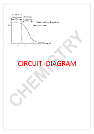


The document is a research project by Himanshu Soni on constructing a transistor switch and analyzing input-output voltage relationships. It includes acknowledgments, intentions, theories, procedures, observations, and conclusions regarding the active and cut-off regions of the transistor. The results reveal the behavior of the transistor acting as a switch in different voltage scenarios.


