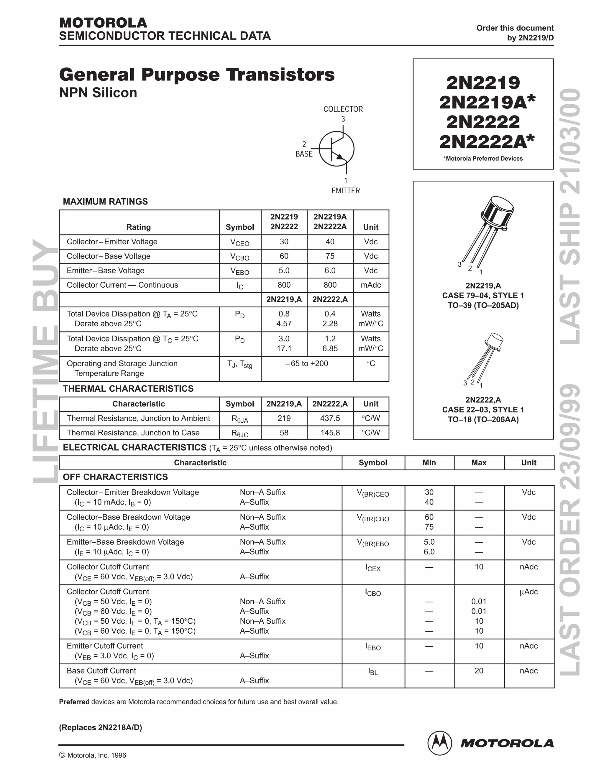
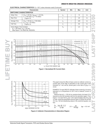
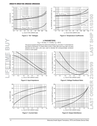
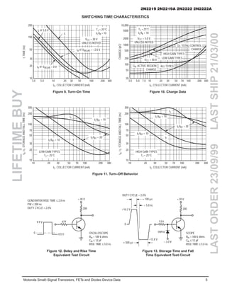
LIFETIMEBUY
LASTORDER23/09/99LASTSHIP21/03/00
1Motorola Small–Signal Transistors, FETs and Diodes Device Data
General Purpose Transistors
NPN Silicon
MAXIMUM RATINGS
Rating Symbol
2N2219
2N2222
2N2219A
2N2222A Unit
Collector–Emitter Voltage VCEO 30 40 Vdc
Collector–Base Voltage VCBO 60 75 Vdc
Emitter–Base Voltage VEBO 5.0 6.0 Vdc
Collector Current — Continuous IC 800 800 mAdc
2N2219,A 2N2222,A
Total Device Dissipation @ TA = 25°C
Derate above 25°C
PD 0.8
4.57
0.4
2.28
Watts
mW/°C
Total Device Dissipation @ TC = 25°C
Derate above 25°C
PD 3.0
17.1
1.2
6.85
Watts
mW/°C
Operating and Storage Junction
Temperature Range
TJ, Tstg –65 to +200 °C
THERMAL CHARACTERISTICS
Characteristic Symbol 2N2219,A 2N2222,A Unit
Thermal Resistance, Junction to Ambient RqJA 219 437.5 °C/W
Thermal Resistance, Junction to Case RqJC 58 145.8 °C/W
ELECTRICAL CHARACTERISTICS (TA = 25°C unless otherwise noted)
Characteristic Symbol Min Max Unit
OFF CHARACTERISTICS
Collector–Emitter Breakdown Voltage Non–A Suffix
(IC = 10 mAdc, IB = 0) A–Suffix
V(BR)CEO 30
40
—
—
Vdc
Collector–Base Breakdown Voltage Non–A Suffix
(IC = 10 µAdc, IE = 0) A–Suffix
V(BR)CBO 60
75
—
—
Vdc
Emitter–Base Breakdown Voltage Non–A Suffix
(IE = 10 µAdc, IC = 0) A–Suffix
V(BR)EBO 5.0
6.0
—
—
Vdc
Collector Cutoff Current
(VCE = 60 Vdc, VEB(off) = 3.0 Vdc) A–Suffix
ICEX — 10 nAdc
Collector Cutoff Current
(VCB = 50 Vdc, IE = 0) Non–A Suffix
(VCB = 60 Vdc, IE = 0) A–Suffix
(VCB = 50 Vdc, IE = 0, TA = 150°C) Non–A Suffix
(VCB = 60 Vdc, IE = 0, TA = 150°C) A–Suffix
ICBO
—
—
—
—
0.01
0.01
10
10
µAdc
Emitter Cutoff Current
(VEB = 3.0 Vdc, IC = 0) A–Suffix
IEBO — 10 nAdc
Base Cutoff Current
(VCE = 60 Vdc, VEB(off) = 3.0 Vdc) A–Suffix
IBL — 20 nAdc
Preferred devices are Motorola recommended choices for future use and best overall value.
Order this document
by 2N2219/D
MOTOROLA
SEMICONDUCTOR TECHNICAL DATA
2N2219
2N2219A
2N2222
2N2222A
2N2219,A
CASE 79–04, STYLE 1
TO–39 (TO–205AD)
1
2
3
*
*
*Motorola Preferred Devices
2N2222,A
CASE 22–03, STYLE 1
TO–18 (TO–206AA)
3 2 1
© Motorola, Inc. 1996
COLLECTOR
3
2
BASE
1
EMITTER
(Replaces 2N2218A/D)
LIFETIMEBUY
LASTORDER23/09/99LASTSHIP21/03/00
2N2219 2N2219A 2N2222 2N2222A
2 Motorola Small–Signal Transistors, FETs and Diodes Device Data
ELECTRICAL CHARACTERISTICS (TA = 25°C unless otherwise noted) (Continued)
Characteristic Symbol Min Max Unit
ON CHARACTERISTICS
DC Current Gain
(IC = 0.1 mAdc, VCE = 10 Vdc) 2N2219,A, 2N2222,A
(IC = 1.0 mAdc, VCE = 10 Vdc) 2N2219,A, 2N2222,A
(IC = 10 mAdc, VCE = 10 Vdc)(1) 2N2219,A, 2N2222,A
(IC = 10 mAdc, VCE = 10 Vdc, TA = –55°C)(1) 2N2219,A, 2N2222,A
(IC = 150 mAdc, VCE = 10 Vdc)(1) 2N2219,A, 2N2222,A
(IC = 150 mAdc, VCE = 1.0 Vdc)(1) 2N2219,A, 2N2222,A
(IC = 500 mAdc, VCE = 10 Vdc)(1) 2N2219, 2N2222
2N2219A, 2N2222A
hFE
35
50
75
35
100
50
30
40
—
—
—
—
300
—
—
—
—
Collector–Emitter Saturation Voltage(1)
(IC = 150 mAdc, IB = 15 mAdc) Non–A Suffix
A–Suffix
(IC = 500 mAdc, IB = 50 mAdc) Non–A Suffix
A–Suffix
VCE(sat)
—
—
—
—
0.4
0.3
1.6
1.0
Vdc
Base–Emitter Saturation Voltage(1)
(IC = 150 mAdc, IB = 15 mAdc) Non–A Suffix
A–Suffix
(IC = 500 mAdc, IB = 50 mAdc) Non–A Suffix
A–Suffix
VBE(sat)
0.6
0.6
—
—
1.3
1.2
2.6
2.0
Vdc
SMALL–SIGNAL CHARACTERISTICS
Current–Gain — Bandwidth Product(2)
(IC = 20 mAdc, VCE = 20 Vdc, f = 100 MHz) All Types, Except
2N2219A, 2N2222A
fT
250
300
—
—
MHz
Output Capacitance(3)
(VCB = 10 Vdc, IE = 0, f = 1.0 MHz)
Cobo — 8.0 pF
Input Capacitance(3)
(VEB = 0.5 Vdc, IC = 0, f = 1.0 MHz) Non–A Suffix
A–Suffix
Cibo
—
—
30
25
pF
Input Impedance
(IC = 1.0 mAdc, VCE = 10 Vdc, f = 1.0 kHz) 2N2219A, 2N2222A
(IC = 10 mAdc, VCE = 10 Vdc, f = 1.0 kHz) 2N2219A, 2N2222A
hje
2.0
0.25
8.0
1.25
kΩ
Voltage Feedback Ratio
(IC = 1.0 mAdc, VCE = 10 Vdc, f = 1.0 kHz) 2N2219A, 2N2222A
(IC = 10 mAdc, VCE = 10 Vdc, f = 1.0 kHz) 2N2219A, 2N2222A
hre
—
—
8.0
4.0
X 10– 4
Small–Signal Current Gain
(IC = 1.0 mAdc, VCE = 10 Vdc, f = 1.0 kHz) 2N2219A, 2N2222A
(IC = 10 mAdc, VCE = 10 Vdc, f = 1.0 kHz) 2N2219A, 2N2222A
hfe
50
75
300
375
—
Output Admittance
(IC = 1.0 mAdc, VCE = 10 Vdc, f = 1.0 kHz) 2N2219A, 2N2222A
(IC = 10 mAdc, VCE = 10 Vdc, f = 1.0 kHz) 2N2219A, 2N2222A
hoe
5.0
15
35
200
mmhos
Collector Base Time Constant
(IE = 20 mAdc, VCB = 20 Vdc, f = 31.8 MHz) A–Suffix
rb′Cc — 150 ps
Noise Figure
(IC = 100 µAdc, VCE = 10 Vdc, RS = 1.0 kΩ,
f = 1.0 kHz) 2N2222A
NF — 4.0 dB
Real Part of Common–Emitter
High Frequency Input Impedance
(IC = 20 mAdc, VCE = 20 Vdc, f = 300 MHz) 2N2219A, 2N2222A
Re(hje) — 60 Ω
1. Pulse Test: Pulse Width v300 ms, Duty Cycle v2.0%.
2. fT is defined as the frequency at which |hfe| extrapolates to unity.
3. 2N5581 and 2N5582 are listed Ccb and Ceb for these conditions and values.
LIFETIMEBUY
LASTORDER23/09/99LASTSHIP21/03/00
2N2219 2N2219A 2N2222 2N2222A
3Motorola Small–Signal Transistors, FETs and Diodes Device Data
ELECTRICAL CHARACTERISTICS (TA = 25°C unless otherwise noted) (Continued)
Characteristic Symbol Min Max Unit
SWITCHING CHARACTERISTICS
Delay Time (VCC = 30 Vdc, VBE(off) = –0.5 Vdc,
IC = 150 mAdc IB1 = 15 mAdc)
td — 10 ns
Rise Time
IC = 150 mAdc, IB1 = 15 mAdc)
(Figure 12) tr — 25 ns
Storage Time (VCC = 30 Vdc, IC = 150 mAdc,
IB1 = IB2 = 15 mAdc)
ts — 225 ns
Fall Time
IB1 = IB2 = 15 mAdc)
(Figure 13) tf — 60 ns
Active Region Time Constant
(IC = 150 mAdc, VCE = 30 Vdc)
(See Figure 11 for 2N2219A, 2N2222A)
TA — 2.5 ns
4.0
3.0
2.0
1.0
0.7
0.5
0.3
0.2
5000.5 0.7 1.0 2.0 3.0 5.0 10 20 30 50 70 100 200 300
IC, COLLECTOR CURRENT (mA)
Figure 1. Normalized DC Current Gain
hFE,NORMALIZEDDCCURRENTGAIN
1.0
0.8
0.6
0.4
0.2
0
0 1.0 2.0 3.0 4.0 5.0
βo/βF, OVERDRIVE FACTOR
VCE,COLLECTOR–EMITTERVOLTAGE(VOLTS)
Figure 2. Collector Characteristics in Saturation Region
This graph shows the effect of base current on collector current. βo
(current gain at the edge of saturation) is the current gain of the
transistor at 1 volt, and βF (forced gain) is the ratio of IC/IBF in a
circuit.
EXAMPLE: For type 2N2219, estimate a base current (IBF) to insure
saturation at a temperature of 25°C and a collector current of
150 mA.
Observe that at IC = 150 mA an overdrive factor of at least 2.5 is
required to drive the transistor well into the saturation region. From
Figure 1, it is seen that hFE @ 1 volt is approximately 0.62 of hFE @
10 volts. Using the guaranteed minimum gain of 100 @ 150 mA and
10 V, βo = 62 and substituting values in the overdrive equation, we
find:
bo
bF
+hFE @ 1.0 V
ICńIBF
2.5 + 62
150ńIBF
IBF [6.0 mA
TJ = 25°C
IC = 300 mA
150 mA
50 mA
TJ = 175°C
25°C
–55°C
VCE = 1.0 V
VCE = 10 V
LIFETIMEBUY
LASTORDER23/09/99LASTSHIP21/03/00
2N2219 2N2219A 2N2222 2N2222A
4 Motorola Small–Signal Transistors, FETs and Diodes Device Data
1.4
1.2
1.0
0.8
0.6
0.4
0.2
0
5000.5 1.0 2.0 5.0 10 20 50 100 200
IC, COLLECTOR CURRENT (mA)
V,VOLTAGE(VOLTS)
V,TEMPERATURECOEFFICIENT(mV/C)°θ
hie,INPUTIMPEDANCE(kOHMS)
h,VOLTAGEFEEDBACKRATIO(X10)re–4
hfe,CURRENTGAIN
h,OUTPUTADMITTANCE(mhos)oem
Figure 3. “On” Voltages
TJ = 25°C
VBE(sat) @ IC/IB = 10
VBE @ VCE = 1.0 V
VCE(sat) @ IC/IB = 10
+1.6
+0.8
0
–0.8
–1.6
–2.4
5000.5 1.0 2.0 5.0 10 20 50 100 200
IC, COLLECTOR CURRENT (mA)
Figure 4. Temperature Coefficients
θVC for VCE(sat)
(25°C to 175°C)
(–55°C to 25°C)
θVB for VBE
h PARAMETERS
VCE = 10 Vdc, f = 1.0 kHz, TA = 25°C
This group of graphs illustrates the relationship between hfe and other “h” parameters for
this series of transistors. To obtain these curves, a high–gain and a low–gain unit were
selected and the same units were used to develop the correspondingly numbered
curves on each graph.
20
10
0.3
0.5
0.7
1.0
2.0
3.0
5.0
7.0
0.1 0.2 0.5 1.0 2.0 5.0 10 20
2
1
IC, COLLECTOR CURRENT (mAdc)
Figure 5. Input Impedance
50
30
20
10
1.0
2.0
3.0
5.0
0.1 0.2 0.5 1.0 2.0 5.0 10 20
IC, COLLECTOR CURRENT (mAdc)
Figure 6. Voltage Feedback Ratio
300
200
100
70
50
30
0.1 0.2 0.5 1.0 2.0 5.0 10 20
IC, COLLECTOR CURRENT (mAdc)
Figure 7. Current Gain
200
100
50
20
10
5.0
0.1 0.2 0.5 1.0 2.0 5.0 10 20
IC, COLLECTOR CURRENT (mAdc)
Figure 8. Output Admittance
1
2
1
2
1
2
LIFETIMEBUY
LASTORDER23/09/99LASTSHIP21/03/00
2N2219 2N2219A 2N2222 2N2222A
5Motorola Small–Signal Transistors, FETs and Diodes Device Data
SWITCHING TIME CHARACTERISTICS
200
10
20
30
50
100
t,TIME(ns)ts,t
CHARGE(pC)
3003.0 5.0 10 20 30 50 100 200
IC, COLLECTOR CURRENT (mA)
Figure 9. Turn–On Time
tr @ 5.0 V
td @ VBE(off) = –2.0 V
tr
td @ VBE(off) = 0 V
TJ = 25°C
IC/IB = 10
VCC = 30 V
UNLESS NOTED
10,000
20
50
100
200
500
1000
2000
5000
3003.0 5.0 10 20 30 50 100 2007.0 70
IC, COLLECTOR CURRENT (mA)
Figure 10. Charge Data
300
200
100
70
50
30
20
10
10 20 30 50 70 100 200 300
IC, COLLECTOR CURRENT (mA)
Figure 11. Turn–Off Behavior
f,STORAGEANDFALLTIME(ns)
ts,tf,STORAGEANDFALLTIME(ns)
ts
tfIC/IB1 = 10
IC/IB1 = 10
IC/IB1 = 20
LOW GAIN TYPES
TJ = 25°C
300
200
100
70
50
30
20
10
10 20 30 50 70 100 200 300
IC, COLLECTOR CURRENT (mA)
HIGH GAIN TYPES
TJ = 25°C
IC/IB1 = 10
IC/IB1 = 10
ts
tf
IC/IB1 = 20
Figure 12. Delay and Rise Time
Equivalent Test Circuit
Figure 13. Storage Time and Fall
Time Equivalent Test Circuit
0
9.9 V
0.5 V
619
+30 V
200
0
≈ 100 µs
+16.2 V
< 5.0 ns
DUTY CYCLE = 2.0%
1.0 k
1N916
–13.8 V
≈ 500 µs
200
–3.0 V
OSCILLOSCOPE
Rin > 100 k ohms
Cin ≤ 12 pF
RISE TIME ≤ 5.0 ns
SCOPE
Rin > 100 k ohms
Cin ≤ 12 pF
RISE TIME ≤ 5.0 ns
TJ = 25°C
IC/IB = 10
VCC = 5.0 V
UNLESS NOTED
QT, TOTAL CONTROL
CHARGE
HIGH GAIN TYPES
LOW GAIN TYPES
VCC = 30 V
QA, ACTIVE REGION
CHARGE
ALL TYPES
GENERATOR RISE TIME ≤ 2.0 ns
PW ≤ 200 ns
DUTY CYCLE = 2.0%
+30 V
LIFETIMEBUY
LASTORDER23/09/99LASTSHIP21/03/00
2N2219 2N2219A 2N2222 2N2222A
6 Motorola Small–Signal Transistors, FETs and Diodes Device Data
PACKAGE DIMENSIONS
CASE 079–04
(TO–205AD)
ISSUE N
NOTES:
1. DIMENSIONING AND TOLERANCING PER ANSI
Y14.5M, 1982.
2. CONTROLLING DIMENSION: INCH.
3. DIMENSION J MEASURED FROM DIMENSION A
MAXIMUM.
4. DIMENSION B SHALL NOT VARY MORE THAN
0.25 (0.010) IN ZONE R. THIS ZONE
CONTROLLED FOR AUTOMATIC HANDLING.
5. DIMENSION F APPLIES BETWEEN DIMENSION
P AND L. DIMENSION D APPLIES BETWEEN
DIMENSION L AND K MINIMUM. LEAD
DIAMETER IS UNCONTROLLED IN DIMENSION
P AND BEYOND DIMENSION K MINIMUM.
STYLE 1:
PIN 1. EMITTER
2. BASE
3. COLLECTOR
SEATING
PLANE
R
E
F
B
C
K
L
P
D 3 PL
–T–
–A–
–H–
M
J
G
2
31
DIM MIN MAX MIN MAX
MILLIMETERSINCHES
A 0.335 0.370 8.51 9.39
B 0.305 0.335 7.75 8.50
C 0.240 0.260 6.10 6.60
D 0.016 0.021 0.41 0.53
E 0.009 0.041 0.23 1.04
F 0.016 0.019 0.41 0.48
G 0.200 BSC 5.08 BSC
H 0.028 0.034 0.72 0.86
J 0.029 0.045 0.74 1.14
K 0.500 0.750 12.70 19.05
L 0.250 ––– 6.35 –––
M 45 BSC 45 BSC
P ––– 0.050 ––– 1.27
R 0.100 ––– 2.54 –––
_ _
MAM0.36 (0.014) H MT
CASE 022–03
(TO–206AA)
ISSUE N
STYLE 1:
PIN 1. EMITTER
2. BASE
3. COLLECTOR
SEATING
PLANE
E
F
B
C
K
L
P
D 3 PL
–T–
–H–
M J
G
2
31
MAM0.36 (0.014) H MT
N
N
–A–
DIM MIN MAX MIN MAX
MILLIMETERSINCHES
A 0.209 0.230 5.31 5.84
B 0.178 0.195 4.52 4.95
C 0.170 0.210 4.32 5.33
D 0.016 0.021 0.406 0.533
E ––– 0.030 ––– 0.762
F 0.016 0.019 0.406 0.483
G 0.100 BSC 2.54 BSC
H 0.036 0.046 0.914 1.17
J 0.028 0.048 0.711 1.22
K 0.500 ––– 12.70 –––
L 0.250 ––– 6.35 –––
M 45 BSC 45 BSC
N 0.050 BSC 1.27 BSC
P ––– 0.050 ––– 1.27
_ _
NOTES:
1. DIMENSIONING AND TOLERANCING PER ANSI
Y14.5M, 1982.
2. CONTROLLING DIMENSION: INCH.
3. DIMENSION J MEASURED FROM DIMENSION A
MAXIMUM.
4. DIMENSION F APPLIES BETWEEN DIMENSION P
AND L. DIMENSION D APPLIES BETWEEN
DIMENSION L AND K MINIMUM. LEAD DIAMETER
IS UNCONTROLLED IN DIMENSION P AND
BEYOND DIMENSION K MINIMUM.
5. DIMENSION E INCLUDES THE TAB THICKNESS.
(TAB THICKNESS IS 0.51(0.002) MAXIMUM).
Motorola reserves the right to make changes without further notice to any products herein. Motorola makes no warranty, representation or guarantee regarding
the suitability of its products for any particular purpose, nor does Motorola assume any liability arising out of the application or use of any product or circuit, and
specifically disclaims any and all liability, including without limitation consequential or incidental damages. “Typical” parameters which may be provided in Motorola
datasheetsand/orspecificationscananddovaryindifferentapplicationsandactualperformancemayvaryovertime. Alloperatingparameters,including“Typicals”
must be validated for each customer application by customer’s technical experts. Motorola does not convey any license under its patent rights nor the rights of
others. Motorola products are not designed, intended, or authorized for use as components in systems intended for surgical implant into the body, or other
applicationsintended to support or sustain life, or for any other application in which the failure of the Motorola product could create a situation where personal injury
ordeath may occur. ShouldBuyerpurchaseoruseMotorolaproductsforanysuchunintendedorunauthorizedapplication,BuyershallindemnifyandholdMotorola
and its officers, employees, subsidiaries, affiliates, and distributors harmless against all claims, costs, damages, and expenses, and reasonable attorney fees
arising out of, directly or indirectly, any claim of personal injury or death associated with such unintended or unauthorized use, even if such claim alleges that
Motorola was negligent regarding the design or manufacture of the part. Motorola and are registered trademarks of Motorola, Inc. Motorola, Inc. is an Equal
Opportunity/Affirmative Action Employer.
How to reach us:
USA/EUROPE/Locations Not Listed: Motorola Literature Distribution; JAPAN: Nippon Motorola Ltd.; Tatsumi–SPD–JLDC, 6F Seibu–Butsuryu–Center,
P.O. Box 20912; Phoenix, Arizona 85036. 1–800–441–2447 or 602–303–5454 3–14–2 Tatsumi Koto–Ku, Tokyo 135, Japan. 03–81–3521–8315
MFAX: RMFAX0@email.sps.mot.com – TOUCHTONE 602–244–6609 ASIA/PACIFIC: Motorola Semiconductors H.K. Ltd.; 8B Tai Ping Industrial Park,
INTERNET: http://Design–NET.com 51 Ting Kok Road, Tai Po, N.T., Hong Kong. 852–26629298
2N2219/D
*2N2219/D*
◊

2 n2222a motorola

  • 1.
    LIFETIMEBUY LASTORDER23/09/99LASTSHIP21/03/00 1Motorola Small–Signal Transistors,FETs and Diodes Device Data General Purpose Transistors NPN Silicon MAXIMUM RATINGS Rating Symbol 2N2219 2N2222 2N2219A 2N2222A Unit Collector–Emitter Voltage VCEO 30 40 Vdc Collector–Base Voltage VCBO 60 75 Vdc Emitter–Base Voltage VEBO 5.0 6.0 Vdc Collector Current — Continuous IC 800 800 mAdc 2N2219,A 2N2222,A Total Device Dissipation @ TA = 25°C Derate above 25°C PD 0.8 4.57 0.4 2.28 Watts mW/°C Total Device Dissipation @ TC = 25°C Derate above 25°C PD 3.0 17.1 1.2 6.85 Watts mW/°C Operating and Storage Junction Temperature Range TJ, Tstg –65 to +200 °C THERMAL CHARACTERISTICS Characteristic Symbol 2N2219,A 2N2222,A Unit Thermal Resistance, Junction to Ambient RqJA 219 437.5 °C/W Thermal Resistance, Junction to Case RqJC 58 145.8 °C/W ELECTRICAL CHARACTERISTICS (TA = 25°C unless otherwise noted) Characteristic Symbol Min Max Unit OFF CHARACTERISTICS Collector–Emitter Breakdown Voltage Non–A Suffix (IC = 10 mAdc, IB = 0) A–Suffix V(BR)CEO 30 40 — — Vdc Collector–Base Breakdown Voltage Non–A Suffix (IC = 10 µAdc, IE = 0) A–Suffix V(BR)CBO 60 75 — — Vdc Emitter–Base Breakdown Voltage Non–A Suffix (IE = 10 µAdc, IC = 0) A–Suffix V(BR)EBO 5.0 6.0 — — Vdc Collector Cutoff Current (VCE = 60 Vdc, VEB(off) = 3.0 Vdc) A–Suffix ICEX — 10 nAdc Collector Cutoff Current (VCB = 50 Vdc, IE = 0) Non–A Suffix (VCB = 60 Vdc, IE = 0) A–Suffix (VCB = 50 Vdc, IE = 0, TA = 150°C) Non–A Suffix (VCB = 60 Vdc, IE = 0, TA = 150°C) A–Suffix ICBO — — — — 0.01 0.01 10 10 µAdc Emitter Cutoff Current (VEB = 3.0 Vdc, IC = 0) A–Suffix IEBO — 10 nAdc Base Cutoff Current (VCE = 60 Vdc, VEB(off) = 3.0 Vdc) A–Suffix IBL — 20 nAdc Preferred devices are Motorola recommended choices for future use and best overall value. Order this document by 2N2219/D MOTOROLA SEMICONDUCTOR TECHNICAL DATA 2N2219 2N2219A 2N2222 2N2222A 2N2219,A CASE 79–04, STYLE 1 TO–39 (TO–205AD) 1 2 3 * * *Motorola Preferred Devices 2N2222,A CASE 22–03, STYLE 1 TO–18 (TO–206AA) 3 2 1 © Motorola, Inc. 1996 COLLECTOR 3 2 BASE 1 EMITTER (Replaces 2N2218A/D)
  • 2.
    LIFETIMEBUY LASTORDER23/09/99LASTSHIP21/03/00 2N2219 2N2219A 2N22222N2222A 2 Motorola Small–Signal Transistors, FETs and Diodes Device Data ELECTRICAL CHARACTERISTICS (TA = 25°C unless otherwise noted) (Continued) Characteristic Symbol Min Max Unit ON CHARACTERISTICS DC Current Gain (IC = 0.1 mAdc, VCE = 10 Vdc) 2N2219,A, 2N2222,A (IC = 1.0 mAdc, VCE = 10 Vdc) 2N2219,A, 2N2222,A (IC = 10 mAdc, VCE = 10 Vdc)(1) 2N2219,A, 2N2222,A (IC = 10 mAdc, VCE = 10 Vdc, TA = –55°C)(1) 2N2219,A, 2N2222,A (IC = 150 mAdc, VCE = 10 Vdc)(1) 2N2219,A, 2N2222,A (IC = 150 mAdc, VCE = 1.0 Vdc)(1) 2N2219,A, 2N2222,A (IC = 500 mAdc, VCE = 10 Vdc)(1) 2N2219, 2N2222 2N2219A, 2N2222A hFE 35 50 75 35 100 50 30 40 — — — — 300 — — — — Collector–Emitter Saturation Voltage(1) (IC = 150 mAdc, IB = 15 mAdc) Non–A Suffix A–Suffix (IC = 500 mAdc, IB = 50 mAdc) Non–A Suffix A–Suffix VCE(sat) — — — — 0.4 0.3 1.6 1.0 Vdc Base–Emitter Saturation Voltage(1) (IC = 150 mAdc, IB = 15 mAdc) Non–A Suffix A–Suffix (IC = 500 mAdc, IB = 50 mAdc) Non–A Suffix A–Suffix VBE(sat) 0.6 0.6 — — 1.3 1.2 2.6 2.0 Vdc SMALL–SIGNAL CHARACTERISTICS Current–Gain — Bandwidth Product(2) (IC = 20 mAdc, VCE = 20 Vdc, f = 100 MHz) All Types, Except 2N2219A, 2N2222A fT 250 300 — — MHz Output Capacitance(3) (VCB = 10 Vdc, IE = 0, f = 1.0 MHz) Cobo — 8.0 pF Input Capacitance(3) (VEB = 0.5 Vdc, IC = 0, f = 1.0 MHz) Non–A Suffix A–Suffix Cibo — — 30 25 pF Input Impedance (IC = 1.0 mAdc, VCE = 10 Vdc, f = 1.0 kHz) 2N2219A, 2N2222A (IC = 10 mAdc, VCE = 10 Vdc, f = 1.0 kHz) 2N2219A, 2N2222A hje 2.0 0.25 8.0 1.25 kΩ Voltage Feedback Ratio (IC = 1.0 mAdc, VCE = 10 Vdc, f = 1.0 kHz) 2N2219A, 2N2222A (IC = 10 mAdc, VCE = 10 Vdc, f = 1.0 kHz) 2N2219A, 2N2222A hre — — 8.0 4.0 X 10– 4 Small–Signal Current Gain (IC = 1.0 mAdc, VCE = 10 Vdc, f = 1.0 kHz) 2N2219A, 2N2222A (IC = 10 mAdc, VCE = 10 Vdc, f = 1.0 kHz) 2N2219A, 2N2222A hfe 50 75 300 375 — Output Admittance (IC = 1.0 mAdc, VCE = 10 Vdc, f = 1.0 kHz) 2N2219A, 2N2222A (IC = 10 mAdc, VCE = 10 Vdc, f = 1.0 kHz) 2N2219A, 2N2222A hoe 5.0 15 35 200 mmhos Collector Base Time Constant (IE = 20 mAdc, VCB = 20 Vdc, f = 31.8 MHz) A–Suffix rb′Cc — 150 ps Noise Figure (IC = 100 µAdc, VCE = 10 Vdc, RS = 1.0 kΩ, f = 1.0 kHz) 2N2222A NF — 4.0 dB Real Part of Common–Emitter High Frequency Input Impedance (IC = 20 mAdc, VCE = 20 Vdc, f = 300 MHz) 2N2219A, 2N2222A Re(hje) — 60 Ω 1. Pulse Test: Pulse Width v300 ms, Duty Cycle v2.0%. 2. fT is defined as the frequency at which |hfe| extrapolates to unity. 3. 2N5581 and 2N5582 are listed Ccb and Ceb for these conditions and values.
  • 3.
    LIFETIMEBUY LASTORDER23/09/99LASTSHIP21/03/00 2N2219 2N2219A 2N22222N2222A 3Motorola Small–Signal Transistors, FETs and Diodes Device Data ELECTRICAL CHARACTERISTICS (TA = 25°C unless otherwise noted) (Continued) Characteristic Symbol Min Max Unit SWITCHING CHARACTERISTICS Delay Time (VCC = 30 Vdc, VBE(off) = –0.5 Vdc, IC = 150 mAdc IB1 = 15 mAdc) td — 10 ns Rise Time IC = 150 mAdc, IB1 = 15 mAdc) (Figure 12) tr — 25 ns Storage Time (VCC = 30 Vdc, IC = 150 mAdc, IB1 = IB2 = 15 mAdc) ts — 225 ns Fall Time IB1 = IB2 = 15 mAdc) (Figure 13) tf — 60 ns Active Region Time Constant (IC = 150 mAdc, VCE = 30 Vdc) (See Figure 11 for 2N2219A, 2N2222A) TA — 2.5 ns 4.0 3.0 2.0 1.0 0.7 0.5 0.3 0.2 5000.5 0.7 1.0 2.0 3.0 5.0 10 20 30 50 70 100 200 300 IC, COLLECTOR CURRENT (mA) Figure 1. Normalized DC Current Gain hFE,NORMALIZEDDCCURRENTGAIN 1.0 0.8 0.6 0.4 0.2 0 0 1.0 2.0 3.0 4.0 5.0 βo/βF, OVERDRIVE FACTOR VCE,COLLECTOR–EMITTERVOLTAGE(VOLTS) Figure 2. Collector Characteristics in Saturation Region This graph shows the effect of base current on collector current. βo (current gain at the edge of saturation) is the current gain of the transistor at 1 volt, and βF (forced gain) is the ratio of IC/IBF in a circuit. EXAMPLE: For type 2N2219, estimate a base current (IBF) to insure saturation at a temperature of 25°C and a collector current of 150 mA. Observe that at IC = 150 mA an overdrive factor of at least 2.5 is required to drive the transistor well into the saturation region. From Figure 1, it is seen that hFE @ 1 volt is approximately 0.62 of hFE @ 10 volts. Using the guaranteed minimum gain of 100 @ 150 mA and 10 V, βo = 62 and substituting values in the overdrive equation, we find: bo bF +hFE @ 1.0 V ICńIBF 2.5 + 62 150ńIBF IBF [6.0 mA TJ = 25°C IC = 300 mA 150 mA 50 mA TJ = 175°C 25°C –55°C VCE = 1.0 V VCE = 10 V
  • 4.
    LIFETIMEBUY LASTORDER23/09/99LASTSHIP21/03/00 2N2219 2N2219A 2N22222N2222A 4 Motorola Small–Signal Transistors, FETs and Diodes Device Data 1.4 1.2 1.0 0.8 0.6 0.4 0.2 0 5000.5 1.0 2.0 5.0 10 20 50 100 200 IC, COLLECTOR CURRENT (mA) V,VOLTAGE(VOLTS) V,TEMPERATURECOEFFICIENT(mV/C)°θ hie,INPUTIMPEDANCE(kOHMS) h,VOLTAGEFEEDBACKRATIO(X10)re–4 hfe,CURRENTGAIN h,OUTPUTADMITTANCE(mhos)oem Figure 3. “On” Voltages TJ = 25°C VBE(sat) @ IC/IB = 10 VBE @ VCE = 1.0 V VCE(sat) @ IC/IB = 10 +1.6 +0.8 0 –0.8 –1.6 –2.4 5000.5 1.0 2.0 5.0 10 20 50 100 200 IC, COLLECTOR CURRENT (mA) Figure 4. Temperature Coefficients θVC for VCE(sat) (25°C to 175°C) (–55°C to 25°C) θVB for VBE h PARAMETERS VCE = 10 Vdc, f = 1.0 kHz, TA = 25°C This group of graphs illustrates the relationship between hfe and other “h” parameters for this series of transistors. To obtain these curves, a high–gain and a low–gain unit were selected and the same units were used to develop the correspondingly numbered curves on each graph. 20 10 0.3 0.5 0.7 1.0 2.0 3.0 5.0 7.0 0.1 0.2 0.5 1.0 2.0 5.0 10 20 2 1 IC, COLLECTOR CURRENT (mAdc) Figure 5. Input Impedance 50 30 20 10 1.0 2.0 3.0 5.0 0.1 0.2 0.5 1.0 2.0 5.0 10 20 IC, COLLECTOR CURRENT (mAdc) Figure 6. Voltage Feedback Ratio 300 200 100 70 50 30 0.1 0.2 0.5 1.0 2.0 5.0 10 20 IC, COLLECTOR CURRENT (mAdc) Figure 7. Current Gain 200 100 50 20 10 5.0 0.1 0.2 0.5 1.0 2.0 5.0 10 20 IC, COLLECTOR CURRENT (mAdc) Figure 8. Output Admittance 1 2 1 2 1 2
  • 5.
    LIFETIMEBUY LASTORDER23/09/99LASTSHIP21/03/00 2N2219 2N2219A 2N22222N2222A 5Motorola Small–Signal Transistors, FETs and Diodes Device Data SWITCHING TIME CHARACTERISTICS 200 10 20 30 50 100 t,TIME(ns)ts,t CHARGE(pC) 3003.0 5.0 10 20 30 50 100 200 IC, COLLECTOR CURRENT (mA) Figure 9. Turn–On Time tr @ 5.0 V td @ VBE(off) = –2.0 V tr td @ VBE(off) = 0 V TJ = 25°C IC/IB = 10 VCC = 30 V UNLESS NOTED 10,000 20 50 100 200 500 1000 2000 5000 3003.0 5.0 10 20 30 50 100 2007.0 70 IC, COLLECTOR CURRENT (mA) Figure 10. Charge Data 300 200 100 70 50 30 20 10 10 20 30 50 70 100 200 300 IC, COLLECTOR CURRENT (mA) Figure 11. Turn–Off Behavior f,STORAGEANDFALLTIME(ns) ts,tf,STORAGEANDFALLTIME(ns) ts tfIC/IB1 = 10 IC/IB1 = 10 IC/IB1 = 20 LOW GAIN TYPES TJ = 25°C 300 200 100 70 50 30 20 10 10 20 30 50 70 100 200 300 IC, COLLECTOR CURRENT (mA) HIGH GAIN TYPES TJ = 25°C IC/IB1 = 10 IC/IB1 = 10 ts tf IC/IB1 = 20 Figure 12. Delay and Rise Time Equivalent Test Circuit Figure 13. Storage Time and Fall Time Equivalent Test Circuit 0 9.9 V 0.5 V 619 +30 V 200 0 ≈ 100 µs +16.2 V < 5.0 ns DUTY CYCLE = 2.0% 1.0 k 1N916 –13.8 V ≈ 500 µs 200 –3.0 V OSCILLOSCOPE Rin > 100 k ohms Cin ≤ 12 pF RISE TIME ≤ 5.0 ns SCOPE Rin > 100 k ohms Cin ≤ 12 pF RISE TIME ≤ 5.0 ns TJ = 25°C IC/IB = 10 VCC = 5.0 V UNLESS NOTED QT, TOTAL CONTROL CHARGE HIGH GAIN TYPES LOW GAIN TYPES VCC = 30 V QA, ACTIVE REGION CHARGE ALL TYPES GENERATOR RISE TIME ≤ 2.0 ns PW ≤ 200 ns DUTY CYCLE = 2.0% +30 V
  • 6.
    LIFETIMEBUY LASTORDER23/09/99LASTSHIP21/03/00 2N2219 2N2219A 2N22222N2222A 6 Motorola Small–Signal Transistors, FETs and Diodes Device Data PACKAGE DIMENSIONS CASE 079–04 (TO–205AD) ISSUE N NOTES: 1. DIMENSIONING AND TOLERANCING PER ANSI Y14.5M, 1982. 2. CONTROLLING DIMENSION: INCH. 3. DIMENSION J MEASURED FROM DIMENSION A MAXIMUM. 4. DIMENSION B SHALL NOT VARY MORE THAN 0.25 (0.010) IN ZONE R. THIS ZONE CONTROLLED FOR AUTOMATIC HANDLING. 5. DIMENSION F APPLIES BETWEEN DIMENSION P AND L. DIMENSION D APPLIES BETWEEN DIMENSION L AND K MINIMUM. LEAD DIAMETER IS UNCONTROLLED IN DIMENSION P AND BEYOND DIMENSION K MINIMUM. STYLE 1: PIN 1. EMITTER 2. BASE 3. COLLECTOR SEATING PLANE R E F B C K L P D 3 PL –T– –A– –H– M J G 2 31 DIM MIN MAX MIN MAX MILLIMETERSINCHES A 0.335 0.370 8.51 9.39 B 0.305 0.335 7.75 8.50 C 0.240 0.260 6.10 6.60 D 0.016 0.021 0.41 0.53 E 0.009 0.041 0.23 1.04 F 0.016 0.019 0.41 0.48 G 0.200 BSC 5.08 BSC H 0.028 0.034 0.72 0.86 J 0.029 0.045 0.74 1.14 K 0.500 0.750 12.70 19.05 L 0.250 ––– 6.35 ––– M 45 BSC 45 BSC P ––– 0.050 ––– 1.27 R 0.100 ––– 2.54 ––– _ _ MAM0.36 (0.014) H MT CASE 022–03 (TO–206AA) ISSUE N STYLE 1: PIN 1. EMITTER 2. BASE 3. COLLECTOR SEATING PLANE E F B C K L P D 3 PL –T– –H– M J G 2 31 MAM0.36 (0.014) H MT N N –A– DIM MIN MAX MIN MAX MILLIMETERSINCHES A 0.209 0.230 5.31 5.84 B 0.178 0.195 4.52 4.95 C 0.170 0.210 4.32 5.33 D 0.016 0.021 0.406 0.533 E ––– 0.030 ––– 0.762 F 0.016 0.019 0.406 0.483 G 0.100 BSC 2.54 BSC H 0.036 0.046 0.914 1.17 J 0.028 0.048 0.711 1.22 K 0.500 ––– 12.70 ––– L 0.250 ––– 6.35 ––– M 45 BSC 45 BSC N 0.050 BSC 1.27 BSC P ––– 0.050 ––– 1.27 _ _ NOTES: 1. DIMENSIONING AND TOLERANCING PER ANSI Y14.5M, 1982. 2. CONTROLLING DIMENSION: INCH. 3. DIMENSION J MEASURED FROM DIMENSION A MAXIMUM. 4. DIMENSION F APPLIES BETWEEN DIMENSION P AND L. DIMENSION D APPLIES BETWEEN DIMENSION L AND K MINIMUM. LEAD DIAMETER IS UNCONTROLLED IN DIMENSION P AND BEYOND DIMENSION K MINIMUM. 5. DIMENSION E INCLUDES THE TAB THICKNESS. (TAB THICKNESS IS 0.51(0.002) MAXIMUM). Motorola reserves the right to make changes without further notice to any products herein. Motorola makes no warranty, representation or guarantee regarding the suitability of its products for any particular purpose, nor does Motorola assume any liability arising out of the application or use of any product or circuit, and specifically disclaims any and all liability, including without limitation consequential or incidental damages. “Typical” parameters which may be provided in Motorola datasheetsand/orspecificationscananddovaryindifferentapplicationsandactualperformancemayvaryovertime. Alloperatingparameters,including“Typicals” must be validated for each customer application by customer’s technical experts. Motorola does not convey any license under its patent rights nor the rights of others. Motorola products are not designed, intended, or authorized for use as components in systems intended for surgical implant into the body, or other applicationsintended to support or sustain life, or for any other application in which the failure of the Motorola product could create a situation where personal injury ordeath may occur. ShouldBuyerpurchaseoruseMotorolaproductsforanysuchunintendedorunauthorizedapplication,BuyershallindemnifyandholdMotorola and its officers, employees, subsidiaries, affiliates, and distributors harmless against all claims, costs, damages, and expenses, and reasonable attorney fees arising out of, directly or indirectly, any claim of personal injury or death associated with such unintended or unauthorized use, even if such claim alleges that Motorola was negligent regarding the design or manufacture of the part. Motorola and are registered trademarks of Motorola, Inc. Motorola, Inc. is an Equal Opportunity/Affirmative Action Employer. How to reach us: USA/EUROPE/Locations Not Listed: Motorola Literature Distribution; JAPAN: Nippon Motorola Ltd.; Tatsumi–SPD–JLDC, 6F Seibu–Butsuryu–Center, P.O. Box 20912; Phoenix, Arizona 85036. 1–800–441–2447 or 602–303–5454 3–14–2 Tatsumi Koto–Ku, Tokyo 135, Japan. 03–81–3521–8315 MFAX: RMFAX0@email.sps.mot.com – TOUCHTONE 602–244–6609 ASIA/PACIFIC: Motorola Semiconductors H.K. Ltd.; 8B Tai Ping Industrial Park, INTERNET: http://Design–NET.com 51 Ting Kok Road, Tai Po, N.T., Hong Kong. 852–26629298 2N2219/D *2N2219/D* ◊