Download to read offline
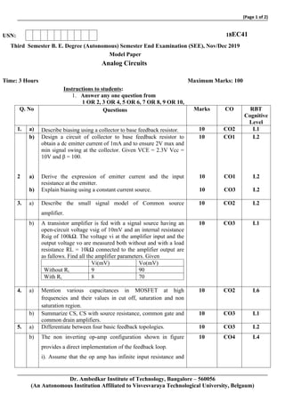
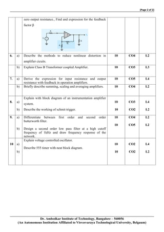

This document is a model paper for the third semester B.E. degree examination in Analog Circuits. It contains 10 questions testing various concepts in analog circuits. Students are instructed to answer any 1 question from each pair of questions 1-10. The questions cover topics such as biasing, small signal modeling, MOSFET capacitances, feedback amplifiers, instrumentation amplifiers, filters, oscillators and timers.