Download to read offline

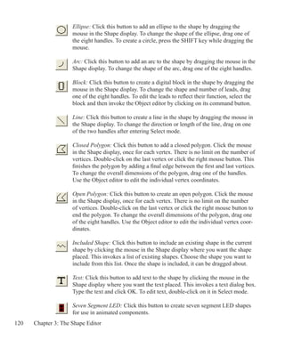
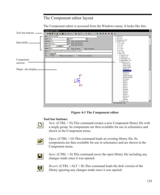
![12
Sample variables 800
Mathematical operators and functions 801
Sample expressions 809
Rules for using operators and variables 812
Chapter 26 - Command Statements 814
.AC 815
.ARRAY 816
.DC 818
.DEFINE 819
.ELIF 821
.ELSE 821
.END 822
.ENDIF 822
.ENDS 822
.ENDSPICE 823
.FUNC 823
.HELP 824
.IC 824
.IF 825
.INCLUDE 826
.LIB 826
.MACRO 827
.MODEL 828
.NODESET 831
.NOISE 832
.OP 832
.OPT[IONS] 833
.PARAM 833
.PARAMETERS 834
.PATH 835
.PLOT 835
.PRINT 835
.PSS 836
.SENS 837
.SPICE 837
.STEP 838
.SUBCKT 839
.TEMP 841
.TF 841
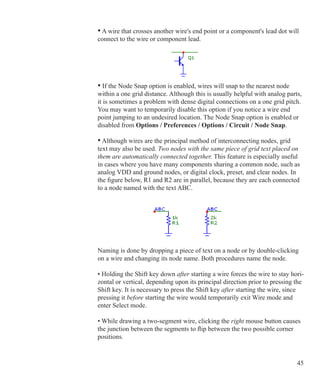
.TIE 842](https://image.slidesharecdn.com/rm102-130625052342-phpapp02/85/Rm10-2-12-320.jpg)
![15
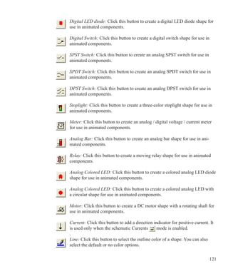
Typographic conventions
Certain typographic conventions are employed to simplify reading and using the
manuals. Here are the guidelines:
1. Named keys are denoted by the key name alone. For example:
Press HOME, then press ENTER.
2. Text that is to be typed by the user is denoted by the text enclosed in double
quotes. For example:
Type in the name TTLINV.
3. Combinations of two keys are shown with the key symbols separated by a plus
sign. For example:
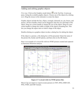
ALT + R
4. Option selection is shown hierarchically. For example this phrase:
Options / Preferences / Options / General / Sound
means the Sound item from the General section of the Options group in the
Preferences dialog box, accessed from the Options menu.
5. Square brackets are used to designate optional entries. For example:
[Low]
6. The characters and bracket required entries. For example:
emitter_lead
7. User entries are shown in italics. For example:
emitter_lead
8. The OR symbol ( | ) designates mutually exclusive alternatives. For
example, PUL | EXP | SIN means PUL or EXP or SIN.](https://image.slidesharecdn.com/rm102-130625052342-phpapp02/85/Rm10-2-15-320.jpg)


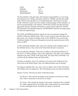
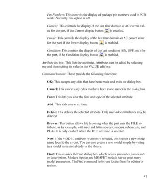
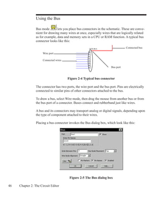
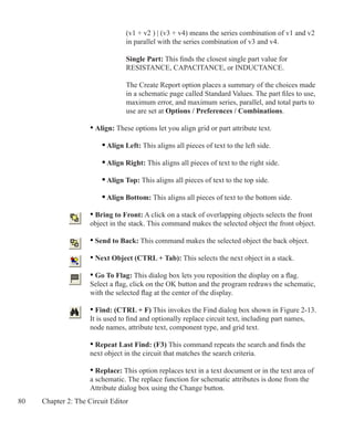
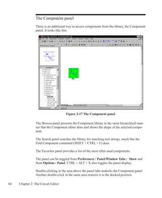
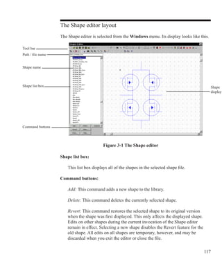
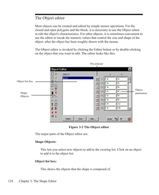
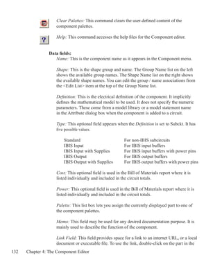
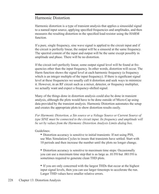
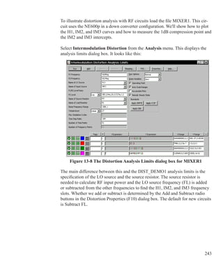
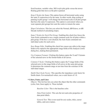
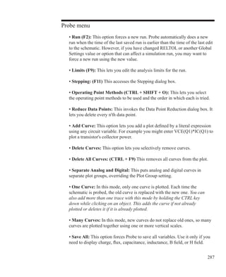
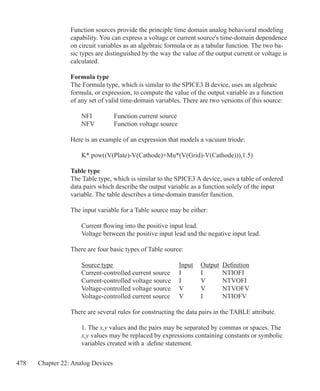
![47
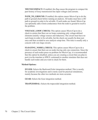
The dialog box has these features:
Part: This field contains the bus connector name. A check box alongside lets
you show or hide the name.
Enter Pin Names: This field contains the pin names, implicitly defining the
number of separate wires / nodes for the bus connector. The names can be
listed separately or using the indicated forms. For example:
A,B,C,D A four pin bus with pins labeled A, B, C, and D
A[1:4] A four pin bus with pins labeled A1, A2, A3, and A4
C[1:4,8,9] A six pin bus with pins labeled C1, C2, C3, C4, C8, and C9
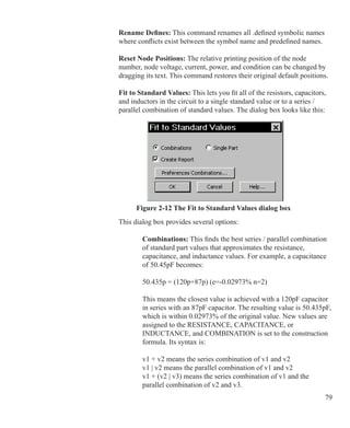
0:7 An eight pin bus with pins labeled 0, 1, 2, 3, 4, 5, 6, and 7
[A,B][1,2] A four pin bus with pins labeled A1, A2, B1, and B2
Grids Between Pins: This specifies the number of grids between pins.
Bus Node Placement: This specifies where to place the bus connector
name. There are three options; top, middle, and bottom.
Wire Node Alignment: This specifies how the wires will emerge from the
connector. There are three options:
Straight: Wires emerge perpendicular to the connector.
Up: Wires slant in one direction.
Down: Wires slant in the opposite direction.
Color: This controls the connector color.
Pin Markers: This check box controls the display of pin markers.
Pin Names: This check box controls the display of pin names.
Enabled: This check box enables/disables the connector.
OK: This accepts the changes and exits the dialog box.
Cancel: This ignores the changes and exits the dialog box.
See ANIM3 for an example of how to use the bus in a circuit.](https://image.slidesharecdn.com/rm102-130625052342-phpapp02/85/Rm10-2-47-320.jpg)
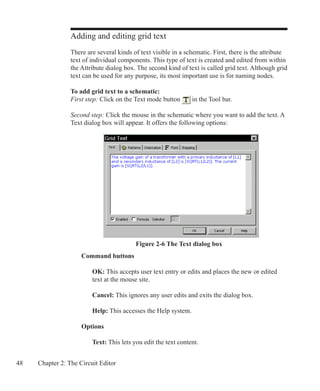
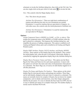
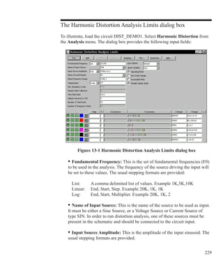
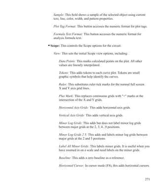
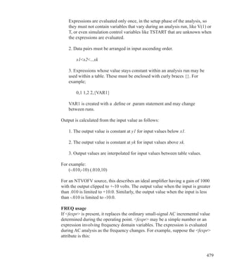
![49
Patterns: This lets you edit the text color, fill (background) color, and
the border width and color.
Orientation: This lets you edit the print order / orientation. There are
four choices. Normal specifies left to right order. Up specifies bottom to
top order. Down specifies top to bottom order. Upside Down specifies
right to left order and upside down orientation.
Font: This lets you edit the text font, size, style, and effects.
Stepping: These options are present only when adding text. They let you
add multiple rows and/or columns of incremented text.
Instances X: This sets the number of rows of text.
Pitch X: This specifies the spacing in number of grids between
rows of text.
Instances Y: This sets the number of columns of text.
Pitch Y: This specifies the spacing in number of grids between
columns of text.
Stepping is used to name wires or nodes with grid text. For example, if
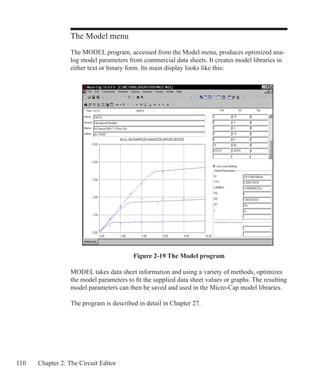
you wanted sixteen names A0, ... A15 vertically arranged, you enter text
of A0, select Instances X = 1, Instances Y = 16, and Pitch Y = 2
(grids).
The stepping tab is present only when you place text. Later, when you
edit a piece of grid text, it is absent since it not needed for editing.
Check boxes:
Enabled: This lets you enable or disable the text. Enabling is important
for text used as a node name and for command text like .DEFINE or
.MODEL statements.
Formula: Checking this tells the program that the text contains a
formula and that the expressions it contains are to be calculated.
Delimiter: This tells the program what character(s) are to be used to
define or delimit the embedded expressions. Although any characters
may be used, brackets [], or braces{} are recommended.](https://image.slidesharecdn.com/rm102-130625052342-phpapp02/85/Rm10-2-49-320.jpg)
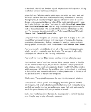
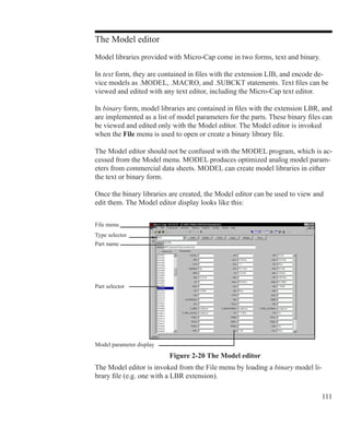
![52 Chapter 2: The Circuit Editor
F0 could now be used in an expression or, in the AC Analysis Limits Frequency
Range, or in a device attribute.
Second Format
The second form is as follows:
text....[formula]...text
For example, if the following four pieces of grid text are entered,
.DEFINE L1 1U
.DEFINE L2 4U
.DEFINE N SQRT(L1/L2)
The voltage gain of a transformer with a primary inductance of [L1] and a
secondary inductance of [L2] is [SQRT(L1/L2)]. The voltage gain is [1/N].
The last piece of text will actually appear as follows:
The voltage gain of a transformer with a primary inductance of 1u
and a secondary inductance of 4u is 0.5. The voltage gain is 2.0.
In this example the delimiter characters are [ and ].
Formula text of this type is calculated only if the Text dialog box's Formula box
is checked.
For both formats of formula text, circuit variables such as V(Out) or I(R1) can
also be used in the equations. The results would not be calculated until an analy-
sis is run.](https://image.slidesharecdn.com/rm102-130625052342-phpapp02/85/Rm10-2-52-320.jpg)


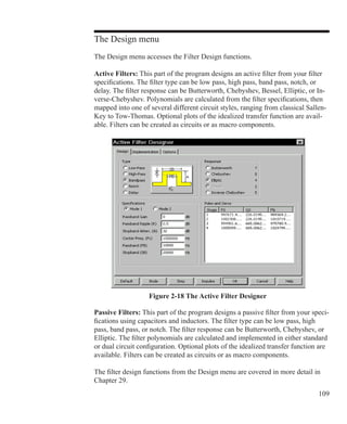


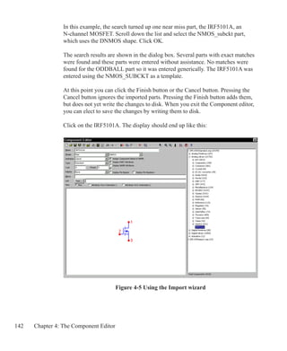

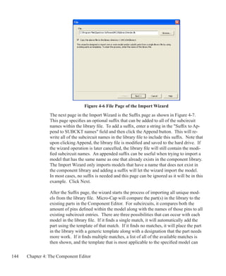
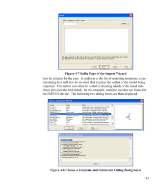

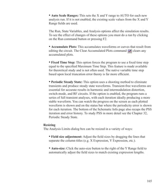
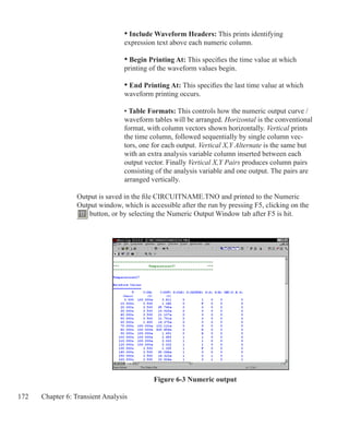
![157
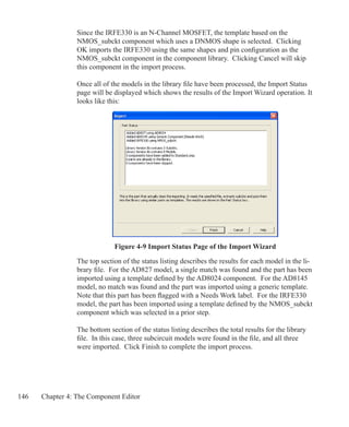
Chapter 6 Transient Analysis
What's in this chapter
Transient analysis requires the repeated iterative solution of a set of nonlinear
time domain equations. The equations are derived from the time-domain models
for each of the components in the circuit. The device models are covered in a
later chapter.
The principal topics described in this chapter include:
• What happens in transient analysis
• Transient Analysis Limits dialog box
• Transient menu
• Initialization
• Using the P key
• Numeric output
Features new in MC10
• Threading is now available for systems with more than one CPU. It can be
used in any analysis mode that involves multiple runs, such as harmonic and
intermodulation distortion, stepping, and Monte Carlo analysis.
• The new Periodic Steady State option provides transient-free waveforms.
• Save, Plot, Don't Plot buttons provide plotting flexibility.
• The State Variables Editor now has numeric format control.
• Branch values may now be used in plot expressions. V(1)@1-V(1)@2 plots
the difference of V(1) between the two branches.
• Cursor values may now be used in formula text expressions. For example,
the formula text [1/(cursorrx-cursorlx)] plots frequency of the expression if
the X variable is T.
• Time-domain Power: When RMS on-schematic display is requested,
transient analysis power is now calculated as P = RMS(V) * RMS(I).
• Time Data Retention: The transient Time Range format of tmax, [tmin] has
been changed to tmax, [tstart]. The analysis always starts at T = 0 but data
points prior to tstart are now discarded after plotting.](https://image.slidesharecdn.com/rm102-130625052342-phpapp02/85/Rm10-2-157-320.jpg)
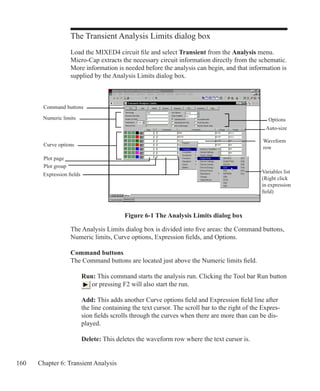
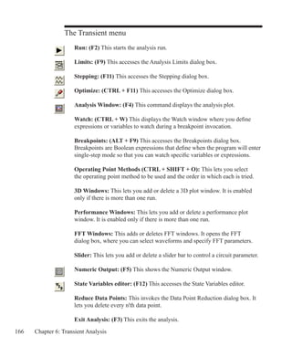
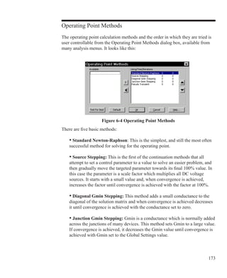
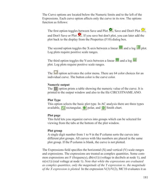
![161
Expand: This expands the text field where the cursor is into a large dialo box
for editing or viewing. To use the feature, click the mouse in the desired field,
and then click the Expand button. Use the Zoom buttons to adjust text size.
Stepping: This invokes the Stepping dialog box. Stepping is reviewed in a
separate chapter.
PSS: This invokes the Periodic Steady State dialog box where you control
PSS parameters. See Chapter 32, Periodic Steady State for more details.
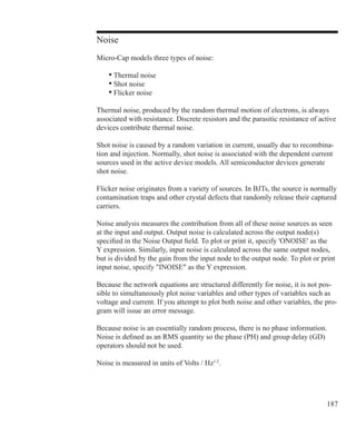
Properties: This command invokes the Properties dialog box which lets you
control the analysis plot window and the way curves are displayed.
Help: This command invokes the Help screen which provides information by
index and topic.
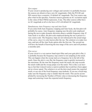
Numeric limits
The Numeric limits field provides control over the analysis time range, time step,
number of printed points, and the temperature(s) to be used.
• Time Range: This field determines the start and stop time for the analysis.
The format of the field is:
tmax [,tstart]
The run starts with time equal to zero and ends when time equals tmax.
Data capture begins for both printing and plotting at tstart.
• Maximum Time Step: This field defines the maximum time step that the
program is allowed to use. The default value, (tmax )/50, is used when the
entry is 0 or blank.
• Number of Points: The contents of this field determine the number of
printed values in the numeric output. The default value is 51. Note that this
number is usually set to an odd value to produce an even print interval. The
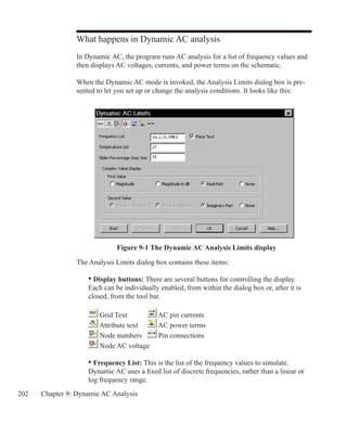
print interval is the time separation between successive printouts. The print
interval used is (tmax - tstart)/([number of points] - 1).
• Temperature: This field specifies the global temperature(s) of the run(s)
in degrees Celsius. This temperature is used for each device unless individual
device temperatures are specified. If the Temperature list box shows Linear
or Log the format is:](https://image.slidesharecdn.com/rm102-130625052342-phpapp02/85/Rm10-2-161-320.jpg)
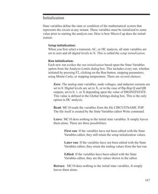
![162 Chapter 6: Transient Analysis
high [ , low [ , step ] ]
The default value of low is high, and the default value of step is
high - low (linear mode) or high/low (log mode). Temperature values
start at low and are either incremented (linear mode) or multiplied (log
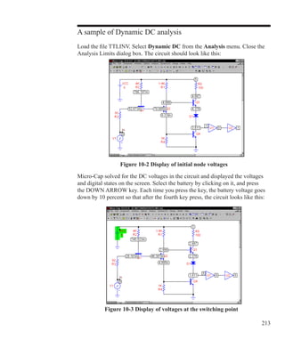
mode) by step until high is reached.
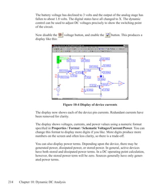
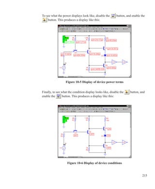
If the Temperature list box shows List the format is:
t1 [ , t2 [ , t3 ] [ ,...]]
where t1, t2,.. are individual values of temperature.
One analysis is done at each specified temperature, producing one curve
branch for each run.
Retrace Runs
This field specifies the number of retrace runs.
Curve options
The Curve options field is located below the Numeric limits field and to the left
of the Expressions field. Each curve option affects only the curve in its row.
The first option toggles between Save and Plot , Save and Don't Plot ,
and Don't Save or Plot . If you save but don't plot, you can later add the
plot back to the display from the Properties (F10) dialog box.
The second option toggles the X-axis between a linear and a log plot.
Log plots require positive scale ranges.
The third option toggles the Y-axis between a linear and a log
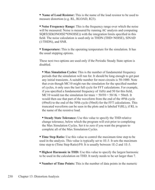
plot. Log plots require positive scale ranges.
Color
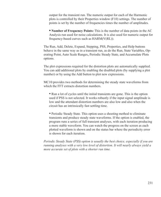
The option activates the color menu. There are 64 color choices for an
individual curve. The button color is the curve color.
Numeric Output
The option prints a table showing the numeric value of the curve. The
number of values printed is set by the Number of Points value. The table is](https://image.slidesharecdn.com/rm102-130625052342-phpapp02/85/Rm10-2-162-320.jpg)
![163
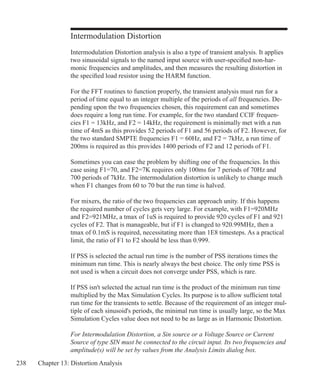
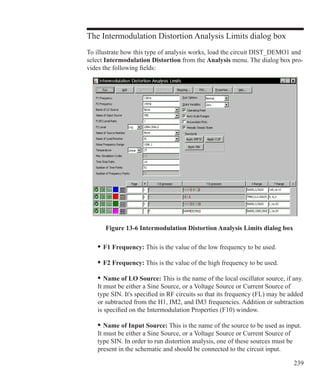
printed to the Output window and saved in the file CIRCUITNAME.TNO.
Plot page
This field lets you organize waveforms into groups which can be selected
for viewing from the tabs at the bottom of the plot window.
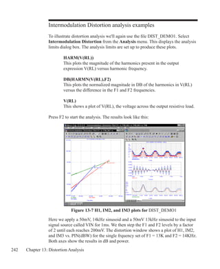
Plot group
A number from 1 to 9 in the (P) column selects the plot group the curve will
be plotted in. All curves with like numbers are placed in the same plot group.
If the P column is blank, the curve is not plotted.
Expression fields
The X Expression and Y Expression fields specify the horizontal (X) and vertical
(Y) expressions. Micro-Cap can evaluate and plot a wide variety of expressions
for either scale. Usually these are single variables like T (time), V(10) (voltage at
node 10), or D(OUT) (digital state of node OUT), but the expressions can be
more elaborate like V(2,3)*I(V1)*sin(2*PI*1E6*T).
Variables list
Clicking the right mouse button in the Y expression field invokes the Variables
list which lets you select variables, constants, functions, operators, and curves, or
expand the field to allow editing long expressions. Clicking the right mouse but-
ton in the other fields invokes a simpler menu showing suitable choices.
The X Range and Y Range fields specify the numeric scales to be used when
plotting the X and Y expressions.
The format is:
high [,low] [,grid spacing] [,bold grid spacing]
low defaults to zero. [,grid spacing] sets the spacing between grids. [,bold
grid spacing] sets the spacing between bold grids. Placing AUTO in the X
or Y range calculates the range automatically. The Auto Scale Ranges option
calculates scales for all ranges during the simulation run and updates the X and
Y Range fields. The Auto Scale (F6) command immediately scales all curves,
without changing the range values, letting you restore them with CTRL + HOME
if desired. Note that grid spacing and bold grid spacing are used only on
linear scales. Logarithmic scales use a natural grid spacing of 1/10 the major grid
values and bold is not used. Auto Scale uses the number of grids specified in the
Properties dialog box (F10) / Scales and Formats / Auto/Static Grids field.](https://image.slidesharecdn.com/rm102-130625052342-phpapp02/85/Rm10-2-163-320.jpg)
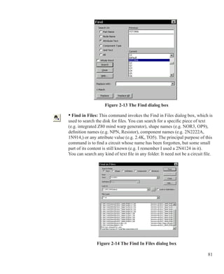
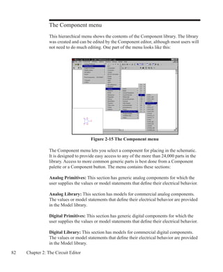
![175
Chapter 7 AC Analysis
What's in this chapter
This chapter describes the AC analysis routines. AC analysis is a linear, small
signal analysis. Before the main AC analysis is run, linearized small signal mod-
els are created for nonlinear components based upon the operating point bias.
Features new in MC10
• Threading is now available for systems with more than one CPU. It can be
used in any analysis mode that involves multiple runs, such as stepping and
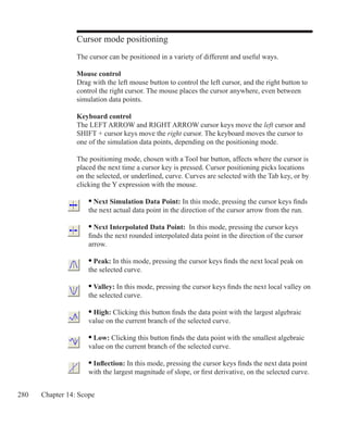
Monte Carlo analysis.
• Save, Plot, Don't Plot buttons provide plotting flexibility.
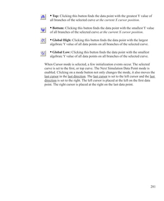
• The State Variables Editor now has numeric format control.
• Branch values may now be used in plot expressions. V(1)@1-V(1)@2 plots
the difference of V(1) between the two branches.
• Cursor values may now be used in plot expressions. For example, the
formula text [1/(cursorrx-cursorlx)] plots frequency of the expression if the
X variable is T.
• Cursor values may now be used in formula text expressions.
• AC power is now calculated as P = V * Conjugate(I).](https://image.slidesharecdn.com/rm102-130625052342-phpapp02/85/Rm10-2-175-320.jpg)
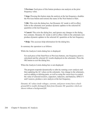
![179
Help: This command calls up the Help system which provides information
by index and topic.
The definition of each item in the Numeric limits field is as follows:
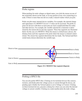
• Frequency Range:
The contents of this field depend upon the type of frequency stepping
selected from the adjacent list box. There are four stepping choices:
• Auto: This method uses the first plot of the first group as a pilot plot.
If, from one frequency point to another, the plot has a vertical change of
greater than Maximum change % of full scale, the frequency step is
reduced, otherwise it is increased. Maximum change % is the value from
the fourth numeric field of the AC Analysis Limits dialog box.
• Linear: This method produces a frequency step such that, with a linear
horizontal scale, the data points are equidistant horizontally. The Number
of Points field sets the total number of data points employed.
• Log: This method produces a frequency step such that with a log
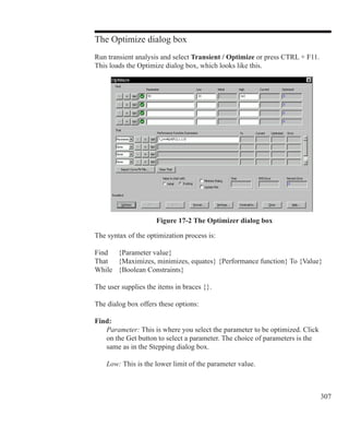
horizontal scale, the data points are equidistant horizontally. The Number
of Points field sets the total number of data points employed.
• List: This method uses a comma-delimited list of frequency points
from the Frequency Range, as in 1E8, 1E7, 5E6.
The Frequency Range field specifies the frequency range for the analysis.
For the List Option:
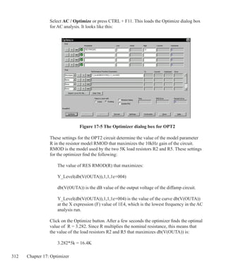
The syntax is Frequency1 [, Frequency2] ... [, FrequencyN].
For Auto, Linear, and Log Options:
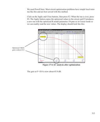
The syntax is Highest Frequency [, Lowest Frequency]. If
Lowest Frequency is unspecified, the program calculates a single data
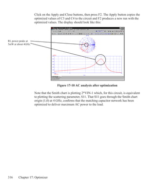
point at Highest Frequency.
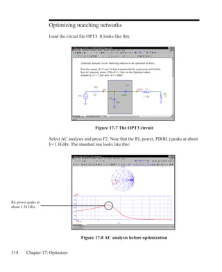
• Number of Points: This determines the number of data points printed in
the Numeric Output window. It also determines the number of data points
actually calculated if Linear or Log stepping is used. If the Auto Step method
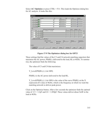
is selected, the number of points actually calculated is controlled by the
Maximum change % value. If Auto is selected, interpolation is used to](https://image.slidesharecdn.com/rm102-130625052342-phpapp02/85/Rm10-2-179-320.jpg)
![180 Chapter 7: AC Analysis
produce the specified number of points. The default value is 51. This number
is usually set to an odd value to produce an even print interval.
For the Linear method, the frequency step and the print interval are:
(Highest Frequency - Lowest Frequency)/(Number of points - 1)
For the Log method, the frequency step is:
(Highest Frequency / Lowest Frequency)1/(Number of points - 1)
• Temperature: This field specifies the global temperature(s) of the run(s)
in degrees Celsius. This temperature is used for each device unless individual
device temperatures are specified. If the Temperature list box shows Linear
or Log the format is:
high [ , low [ , step ] ]
The default value of low is high, and the default value of step is
high - low (linear mode) or high/low (log mode). Temperature values
start at low and are either incremented (linear mode) or multiplied (log
mode) by step until high is reached.
If the Temperature list box shows List the format is:
t1 [ , t2 [ , t3 ] [ ,...]]
where t1, t2,.. are individual values of temperature.
One analysis is done at each specified temperature, producing one curve
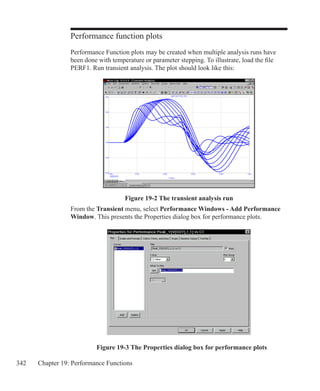
branch for each run.
• Maximum Change %: This value controls the frequency step used when
Auto is selected for the Frequency Step method.
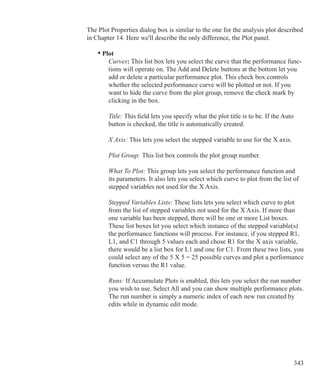
• Noise Input: This is the name of the input source to be used for noise
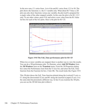
calculations. If the INOISE and ONOISE variables are not used in the
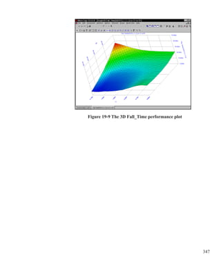
expression fields, this field is ignored.
• Noise Output: This field holds the name(s) or number(s) of the output
node(s) to be used for noise calculations. If the INOISE and ONOISE
variables are not used in the expression fields, this field is ignored.](https://image.slidesharecdn.com/rm102-130625052342-phpapp02/85/Rm10-2-180-320.jpg)
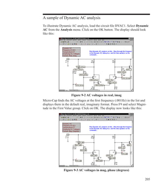
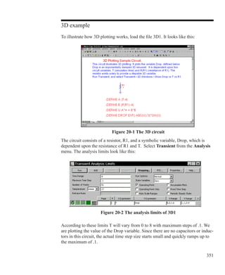
![182 Chapter 7: AC Analysis
a complex quantity, then plots the magnitude of the final result. It is not possible
to plot a complex quantity directly versus frequency. You can plot the imaginary
part of an expression versus its real part (Nyquist plot), or you can plot the real,
magnitude, or imaginary parts versus frequency (Bode plot).
The scale ranges specify the scales to use when plotting the X and Y expressions.
The range format is:
high [,low] [,grid spacing] [,bold grid spacing]
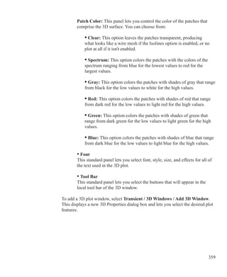
low defaults to zero. [,grid spacing] sets the spacing between grids. [,bold
grid spacing] sets the spacing between bold grids. Placing AUTO in the X or
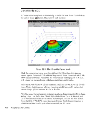
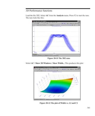
Y scale range calculates its range automatically. The Auto Scale Ranges option
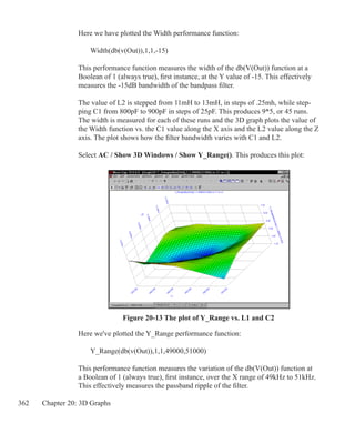
calculates scales for all ranges during the simulation run and updates the X and
Y Range fields. The Auto Scale (F6) command immediately scales all curves,
without changing the range values, letting you restore them with CTRL + HOME
if desired. Note that grid spacing and bold grid spacing are used only on
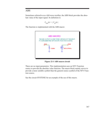
linear scales. Logarithmic scales use a natural grid spacing of 1/10 the major grid
values and bold is not used. Auto Scale uses the number of grids specified in the
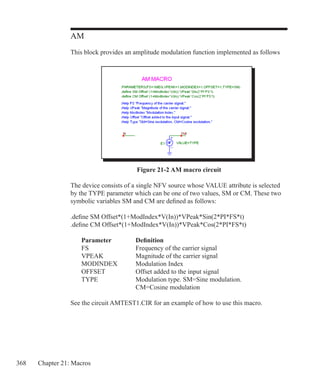
Properties dialog box (F10) / Scales and Formats / Auto/Static Grids field.
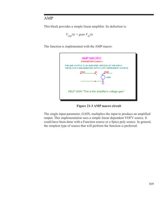
Clicking the right mouse button in the Y expression field invokes the Variables
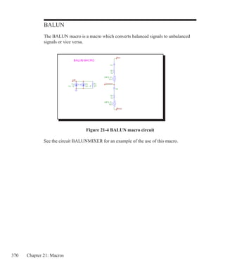
list. It lets you select variables, constants, functions, and operators, or expand the
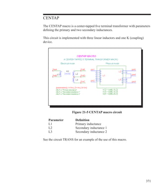
field to allow editing long expressions. Clicking the right mouse button in the
other fields invokes a simpler menu showing suitable choices.
The Options group includes:
• Run Options
• Normal: This runs the simulation without saving it to disk.
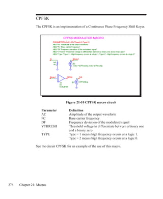
• Save: This runs the simulation and saves it to disk.
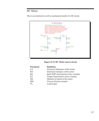
• Retrieve: This loads a previously saved simulation and plots and
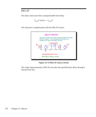
prints it as if it were a new run.
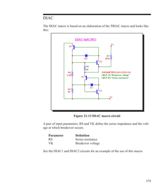
• State Variables: These options determine what happens to the time
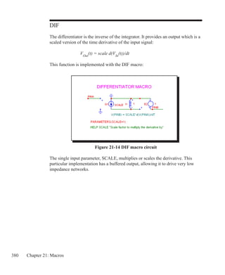
domain state variables (DC voltages, currents, and digital states) prior to
the optional operating point.
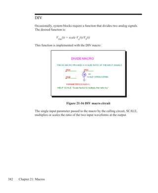
• Zero: This sets the state variable initial values (node voltages, inductor
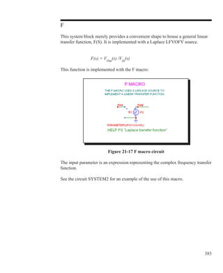
currents, digital states) to zero or X.](https://image.slidesharecdn.com/rm102-130625052342-phpapp02/85/Rm10-2-182-320.jpg)

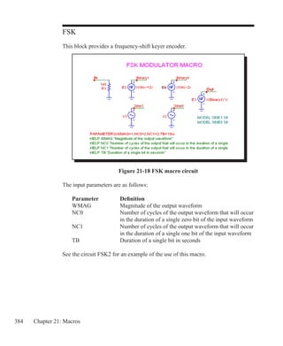
![193
Help: This command calls up the Help system.
The definition of each field in the Numeric limits are as follows:
• Variable 1: This row specifies the Method, Name, and Range fields for
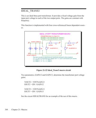
variable 1. Its value is usually plotted along the X axis. Each value produces
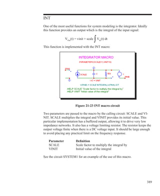
a minimum of one data point per curve. There are four column fields for this
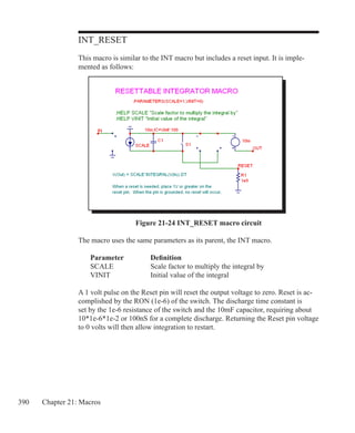
variable.
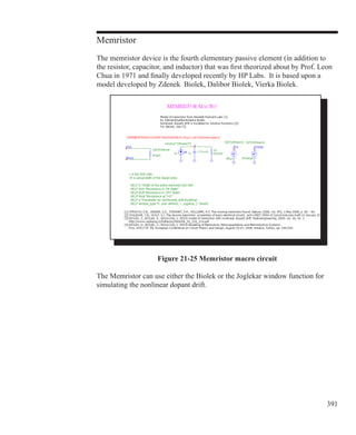
• Method: This field specifies one of four methods for stepping the
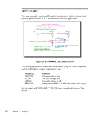
variable: Auto, Linear, Log, or List.
• Auto: In Auto mode the rate of step size is adjusted to keep the
point-to-point change less than Maximum Change % value.
• Linear: This mode uses the following syntax from the Range
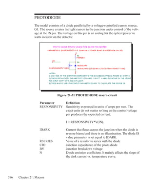
column for this row:
end [,start [,step] ]
Start defaults to 0.0. Step defaults to (start - end)/50. Variable 1
starts at start. Subsequent values are computed by adding step until
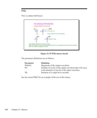
end is reached.
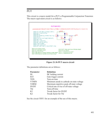
• Log: Log mode uses the following syntax from the Range column
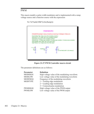
for this row:
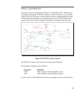
end [,start [,step] ]
Start defaults to end/10. Step defaults to exp(ln(end/start)/10).
Variable 1 starts at start. Subsequent values are computed by
multiplying by step until end is reached.
• List: List mode uses the following syntax from the Range column
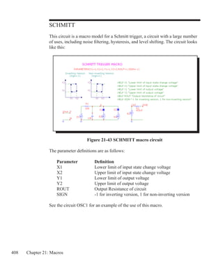
for this row:
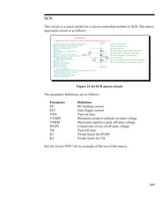
v1 [,v2 [,v3] ...[,vn] ]
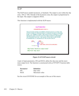
The variable is simply set to each of the values v1, v2, .. vn.](https://image.slidesharecdn.com/rm102-130625052342-phpapp02/85/Rm10-2-193-320.jpg)
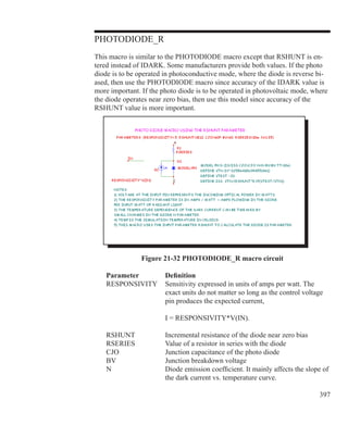
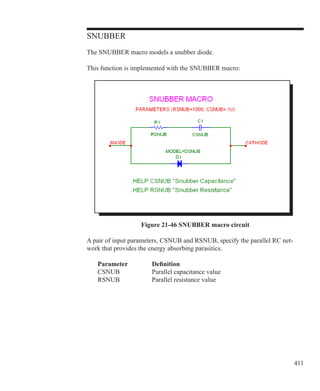
![194 Chapter 8: DC Analysis
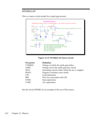
• Name: This field specifies the name of variable 1. The variable
itself may be a source value, temperature, a model parameter, or a
symbolic parameter (one created with a .DEFINE statement). Model
parameter stepping requires both a model name and a model
parameter name.
• Range: This field specifies the numeric range for the variable. The
range syntax depends upon the Method field described above.
• Variable 2: This row specifies the Method, Name, and Range fields for
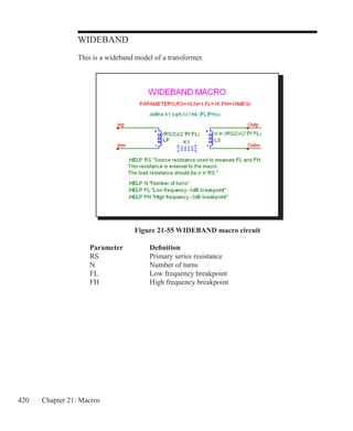
variable 2. The syntax is the same as for variable 1, except that the stepping
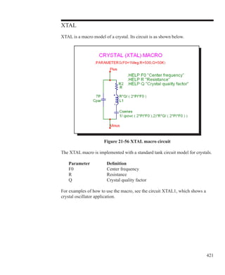
options include None and exclude Auto. Step defaults to (end - start)/10.
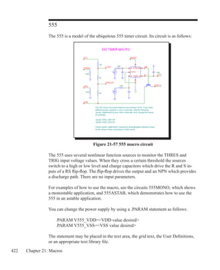
Each value of variable 2 produces a separate branch of the curve.
• Temperature: This controls the temperature of the run. The fields are:
• Method: This list box specifies one of the methods for stepping the
temperature: If the list box shows Linear or Log the format is:
high [ , low [ , step ] ]
The default value of low is high, and the default value of step is
high - low (linear mode) or high/low (log mode). Temperature
values start at low and are either incremented (linear mode) or
multiplied (log mode) by step until high is reached.
If the list box shows List the format is:
t1 [ , t2 [ , t3 ] [ ,...]]
where t1, t2,.. are individual values of temperature.
One analysis is done at each specified temperature, producing one curve
branch for each run. When temperature is selected as one of the
stepped variables (variable 1 or variable 2) this field is not available.
• Range: This field specifies the range for the temperature variable. The
range syntax depends upon the Method field described above.
• Number of Points: This is the number of data points to be interpolated and
printed if numeric output is requested. This number defaults to 51 and is](https://image.slidesharecdn.com/rm102-130625052342-phpapp02/85/Rm10-2-194-320.jpg)
![196 Chapter 8: DC Analysis
The Expressions field is used to specify the horizontal (X) and vertical (Y) scale
ranges and expressions. Some common expressions used are VCE(Q1) (collector
to emitter voltage of transistor Q1) or IB(Q1) (base current of transistor Q1).
The X Range and Y Range fields specify the scales to be used when plotting the
X and Y expressions. The range format is:
high [,low] [,grid spacing] [,bold grid spacing]
low defaults to zero. [,grid spacing] sets the spacing between grids. [,bold
grid spacing] sets the spacing between bold grids. Placing AUTO in the scale
range calculates that individual range automatically. The Auto Scale Ranges op-
tion calculates scales for all ranges during the simulation run and updates the X
and Y Range fields.
The Auto Scale (F6) command immediately scales all curves, without chang-
ing the range values, letting you restore them with CTRL + HOME if desired.
Note that grid spacing and bold grid spacing are used only on linear scales.
Logarithmic scales use a natural grid spacing of 1/10 the major grid values and
bold is not used. Auto Scale uses the number of grids specified in the Properties
dialog box (F10) / Scales and Formats / Auto/Static Grids field.
Clicking the right mouse button in the Y expression field invokes the Variables
list which lets you select variables, constants, functions, and operators, or expand
the field to allow editing long expressions. Clicking the right mouse button in the
other fields invokes a simpler menu showing suitable choices.
The Options area is below the Numeric limits. The Auto Scale Ranges option has
a check box.
The options available from here are:
• Run Options
• Normal: This runs the simulation without saving it to disk.
• Save: This runs the simulation and saves it to disk.
• Retrieve: This loads a previously saved simulation and plots and
prints it as if it were a new run.
• Auto Scale Ranges: This sets the X and Y range to auto every time a
simulation is run. If disabled, the values from the range fields will be used.](https://image.slidesharecdn.com/rm102-130625052342-phpapp02/85/Rm10-2-196-320.jpg)


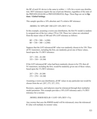
![322 Chapter 18: Monte Carlo Analysis
How Monte Carlo works
Monte Carlo works by analyzing many circuits. Each circuit is constructed of
components randomly selected from populations matching the user-specified
tolerances and distribution type. Tolerances are applied to parameters. Model
parameters can have DEV and LOT tolerances. Symbolic parameters, batteries,
and the parameters of the Voltage Source and the Current Source can be LOT
toleranced only. Tolerances are specified as an actual value or as a percentage of
the nominal parameter value.
Both absolute (LOT) and relative (DEV) tolerances can be specified. A LOT tol-
erance is applied absolutely to each device. A DEV tolerance is then applied to
the first through last device relative to the LOT toleranced value originally cho-
sen for the first device. In other words, the first device in the list receives a LOT
tolerance, if one was specified. All devices, including the first, then receive the
first device's value plus or minus the DEV tolerance. DEV tolerances provide a
means for having some devices track in their critical parameter values.
Both tolerances are specified by including the key words LOT or DEV after the
model parameter:
[LOT[td]=value[%]] [DEV[td]=value[%]]
For example, this model statement specifies a 10% absolute tolerance to the for-
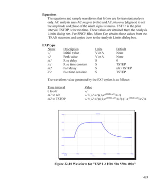
ward beta of the transistor N1:
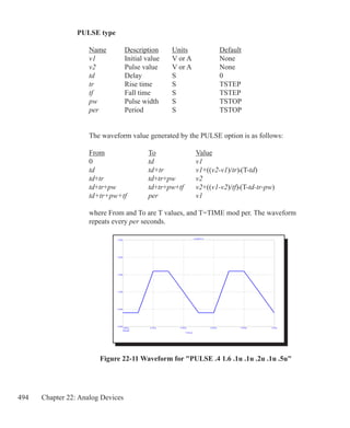
.MODEL N1 NPN (BF=300 LOT=10%)
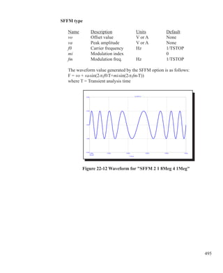
In this example, for a worst case distribution, each transistor using the N1 model
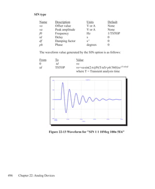
statement has a forward beta of either 270 or 330. For a Gaussian distribution,
a random value would be selected from a distribution with a standard deviation
of 30/SD (SD is the number of standard deviations in the tolerance band). For a
uniform distribution, a random value would be selected from a distribution with a
half-width of 30.
This example specifies a 1% relative tolerance to the BF of the N1 model:
.MODEL N1 NPN (BF=300 DEV=1%)
The DEV value specifies the relative percentage variation of a parameter. A rela-
tive tolerance of 0% implies perfect tracking. A 1.0% DEV tolerance implies that](https://image.slidesharecdn.com/rm102-130625052342-phpapp02/85/Rm10-2-322-320.jpg)
![324 Chapter 18: Monte Carlo Analysis
[td] specifies the tracking and distribution, using the following format:
[/lot#][/distribution name]
These specifications must follow the keywords DEV and LOT without spaces
and must be separated by /.
lot# specifies which of one hundred random number generators, numbered 0
through 99, are used to calculate parameter values. This lets you correlate param-
eters of an individual model statement (e.g. RE and RC of a particular NPN tran-
sistor model) as well as parameters between models (e.g. BF of NPNA and BF of
NPNB). The DEV random number generators are distinct from the LOT random
number generators. Tolerances without lot# get unique random numbers.
distribution name specifies the distribution. It can be any of the following:
Keyword Distribution
UNIFORM Equal probability distribution
GAUSS Normal or Gaussian distribution
WCASE Worst case distribution
If a distribution is not specified in [td], the distribution specified in the Monte
Carlo dialog box is used.
To illustrate the use of lot#, suppose we have the following circuit:
In this example, Q1's RE value will be uncorrelated with Q2's RE value. During
the Monte Carlo runs, each will receive random uncorrelated tolerances.
Figure 18-1 Uncorrelated RE values](https://image.slidesharecdn.com/rm102-130625052342-phpapp02/85/Rm10-2-324-320.jpg)
![325
Now consider this circuit:
Figure 18-2 Using lot# to correlate RE values
Here, the presence of LOT/1 in both RE tolerance specs forces the LOT tolerance
of the RE values to be the same. The values themselves won't be the same since
their nominal values (1.0 and 2.0) are different.
DEV can also use [td] specifications. Consider this circuit.
Here the LOT toleranced RE values will track perfectly, but when the DEV toler-
ance is added, the values will be different due to the use of different generators
for DEV.
Figure 18-3 Using lot# in DEV and LOT](https://image.slidesharecdn.com/rm102-130625052342-phpapp02/85/Rm10-2-325-320.jpg)
![326 Chapter 18: Monte Carlo Analysis
Tolerancing symbolic parameters
Symbolic parameters, those created with a .DEFINE statement, may also be tol-
eranced. The format is as follows:
.DEFINE [{lotspec}] varname expr
where the format of lotspec is similar to that for other parameters except there is
no DEV tolerance. With symbolic variables, there is only one instance so DEV
tolerancing cannot be used.
[LOT[td]=value[%]]
[td] specifies the tracking and distribution, using the usual format:
[/lot#][/distribution name]
For example,
.DEFINE {LOT/1/GAUSS=10%} RATE 100
This defines a variable called RATE that has a Gaussian distribution with a LOT
tolerance of 10% and its tolerances are based on random number generator 1.
Here is another example:
.DEFINE {LOT/3/UNIFORM=20%} VOLTAIRE 100
This defines a variable called VOLTAIRE with a nominal value of 100. It has a
uniform distribution with a LOT tolerance of 20%. Its LOT tolerance is based on
the random number generator 3.
AGAUSS, GAUSS, UNIF, and AUNIF functions can also be used to specify dis-
tributions. For example, if a resistor VALUE attribute is agauss(1k,100,2), this
specifies a 1k resistor with a tolerance of 100 at 2 standard deviations. The stan-
dard deviation is 50 = 100/2 in this case.](https://image.slidesharecdn.com/rm102-130625052342-phpapp02/85/Rm10-2-326-320.jpg)
![329
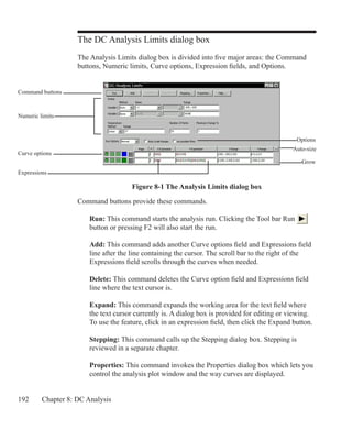
Options
The Monte Carlo options dialog box provides these choices:
• Distribution to Use: This specifies the default distribution to use for all
LOT and DEV tolerances that do not specify a distribution with [td].
• Gaussian distributions are governed by the standard equation:
f(x) = e-.5•s•s
/σ(2•π).5
Where s = x-µ/σ and µ is the nominal parameter value, σ is the standard
deviation, and x is the independent variable.
• Uniform distributions have equal probability within the tolerance
limits. Each value from minimum to maximum is equally likely.
• Worst case distributions have a 50% probability of producing the
minimum and a 50% probability of producing the maximum.
• Status: Monte Carlo analysis is enabled by selecting the On option. To
disable it, click the Off option.
• Number of Runs: The number of runs determines the confidence in the
statistics produced. More runs produce a higher confidence that the mean and
standard deviation accurately reflect the true distribution. Generally, from 30
to 300 runs are needed for a high confidence. The maximum is 30000 runs.
• Show Zero Tolerance Curve: If this option is enabled, the first run
tolerances are set to zero to provide a kind of baseline or reference curve.
• Eliminate Outliers: If this option is enabled, any values outside of the
tolerance band are eliminated. This only applies to Gaussian distributions.
• Report When: This field specifies when to report a failure. The routine
generates a failure report in the numeric output file when the Boolean
expression in this field is true. The field must contain a performance
function specification. For example, this expression
rise_time(V(1),1,2,0.8,1.4)10ns](https://image.slidesharecdn.com/rm102-130625052342-phpapp02/85/Rm10-2-329-320.jpg)
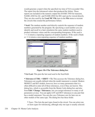


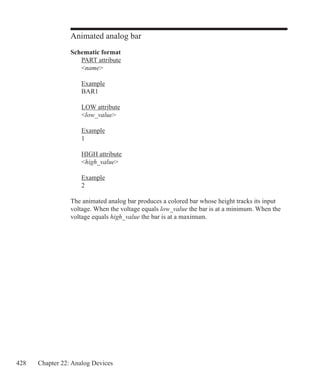
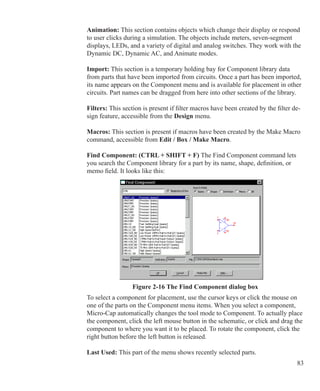
![429
Animated analog LED
Schematic format
PART attribute
name
Example
LED2
COLOR attribute
color name , on voltage , on current , [rs] , [cjo]
Example
Red,1.7,0.015,250m,30p
This device is a light emitting diode whose color appears when the diode voltage
equals or exceeds on voltage. It is modeled as a conventional diode with the
model parameters RS set to [rs] and CJO set to [cjo]. Other model parameters are
adjusted so that the diode voltage and current match the specified on voltage
and on current. [rs] defaults to .500. [cjo] defaults to 20pF.
The choice of color is controlled by the user-selected palette color associated
with color name. To change the color name or actual on-screen color, double
click on a LED, then click on the COLOR attribute, then on the LED Color but-
ton in the Attribute dialog box. This invokes the LED Color dialog box which lets
you edit the existing LED COLOR attributes or add additional ones. The follow-
ing are supplied with the original Micro-Cap library.
YELLOW, 2.0, 15m, 500m, 20pF
GREEN, 2.1, 15m, 500m, 20pF
BLUE, 3.4, 12m, 500m, 20pF
RED, 1.7, 15m, 500m, 20pF](https://image.slidesharecdn.com/rm102-130625052342-phpapp02/85/Rm10-2-429-320.jpg)

![441
Bipolar transistor (Standard Gummel Poon Level=1)
SPICE format
Syntax
Qname collector base emitter [substrate]
+model name [area] [OFF] [IC=vbe[,vce]]
Examples
Q1 5 7 9 2N3904 1 OFF IC=0.65,0.35
Q2 5 7 9 20 2N3904 2.0
Q3 C 20 OUT [SUBS] 2N3904
Schematic format
PART attribute
name
Examples
Q1
BB1
VALUE attribute
[area] [OFF] [IC=vbe[,vce]]
Example
1.5 OFF IC=0.65,0.35
MODEL attribute
model name
Example
2N2222A
The initialization, 'IC=vbe[,vce]', assigns initial voltages to the junctions in
transient analysis if no operating point is done (or if the UIC flag is set). Area
multiplies or divides parameters as shown in the model parameters table. The
OFF keyword forces the BJT off for the first iteration of the operating point.
Model statement forms
.MODEL model name NPN ([model parameters])
.MODEL model name PNP ([model parameters])
.MODEL model name LPNP ([model parameters])](https://image.slidesharecdn.com/rm102-130625052342-phpapp02/85/Rm10-2-441-320.jpg)
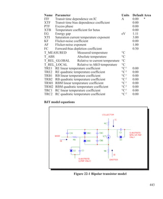
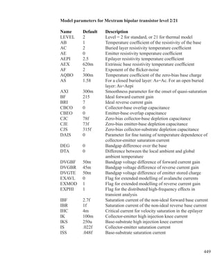
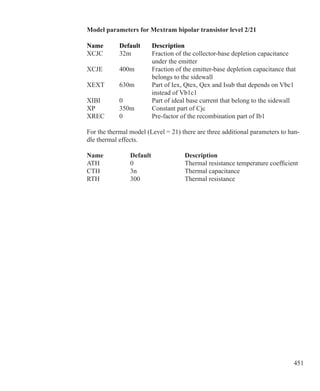
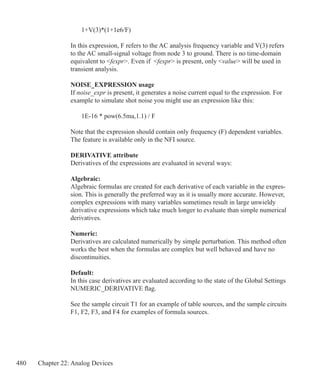
![444 Chapter 22: Analog Devices
Definitions
The model parameters IS, IKF, ISE, IKR, ISC, ISS, IRB, CJC, CJE, CJS, and ITF
are multiplied by [area] and the model parameters RC, RE, RB, and RBM are
divided by [area] prior to their use in the equations below.
T is the device operating temperature and Tnom is the temperature at which the
model parameters are measured. Both are expressed in degrees Kelvin. T is set
to the analysis temperature from the Analysis Limits dialog box. TNOM is de-
termined by the Global Settings TNOM value, which can be overridden with a
.OPTIONS statement. T and Tnom may both be customized for each model by
specifying the parameters T_MEASURED, T_ABS, T_REL_GLOBAL, and T_
REL_LOCAL. For more details on how device operating temperatures and Tnom
temperatures are calculated, see the .MODEL section of Chapter 26, Command
Statements.
The substrate node is optional and, if not specified, is connected to ground. If, in
a SPICE file, the substrate node is specified and is an alphanumeric name, it must
be enclosed in square brackets.
The model types NPN and PNP are used for vertical transistor structures and the
LPNP is used for lateral PNP structures. The isolation diode DJ and capacitance
CJ are connected from the substrate node to the internal collector node for NPN
and PNP model types, and from the substrate node to the internal base node for
the LPNP model type.
When adding new four terminal BJT components to the Component library, use
NPN4 or PNP4 for the Definition field.
When a PNP4 component is placed in a schematic, the circuit is issued an LPNP
model statement. If you want a vertical PNP4, change the LPNP to PNP.
VT = k•T/q
VBE = Internal base to emitter voltage
VBC = Internal base to collector voltage
VCS = Internal collector to substrate voltage
In general, X(T) = Temperature adjusted value of parameter X
Temperature effects
EG(T) = EG - .000702•T2
/(T+1108)
IS(T) = IS•e((T/Tnom-1)•EG/(VT))
•(T/Tnom)(XTI)
ISE(T) = (ISE/(T/Tnom)XTB
)•e((T/Tnom-1)•EG/(NE•VT))
•(T/Tnom)(XTI/NE)
ISC(T) = (ISC/(T/Tnom)XTB
)•e((T/Tnom-1)•EG/(NC•VT))
•(T/Tnom)(XTI/NC)](https://image.slidesharecdn.com/rm102-130625052342-phpapp02/85/Rm10-2-444-320.jpg)
![447
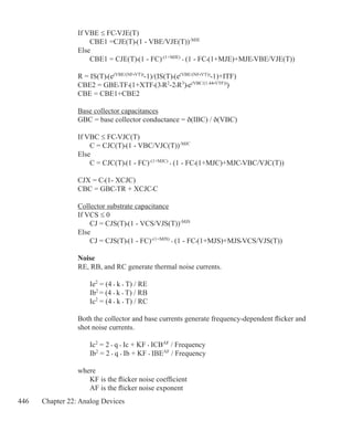
Bipolar transistor (Philips Mextram Level = 2 or 21)
SPICE format
Syntax
Qname collector base emitter [substrate] [thermal]
+model name
+ MULT=no_parallel
Examples
Q1 1 2 3 MM1
Q2 1 2 3 4 MM2
Q3 1 2 3 4 5 MM3
Q4 1 2 3 4 5 MM3 MULT=20
Schematic format
PART attribute
name
Examples
Q1
BB1
VALUE attribute
MULT=no_parallel
Example
MULT=100
MODEL attribute
model name
Example
MLX
Model statement form
.MODEL model name NPN (LEVEL=2 [model parameters])
.MODEL model name NPN (LEVEL=21 [model parameters])
Example of standard model
.MODEL MODN NPN (LEVEL=2 ...)](https://image.slidesharecdn.com/rm102-130625052342-phpapp02/85/Rm10-2-447-320.jpg)
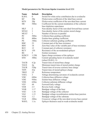
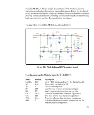
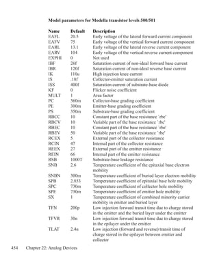
![452 Chapter 22: Analog Devices
Bipolar transistor (Philips Modella Level = 500 or 501)
SPICE format
Syntax
Qname collector base emitter [substrate] [thermal]
+model name
+ MULT=no_parallel
Examples
Q1 1 2 3 MM1
Q2 1 2 3 4 MM2
Q3 1 2 3 4 5 MM3
Q4 1 2 3 4 5 MM3 MULT=20
Schematic format
PART attribute
name
Example
Q1
VALUE attribute
MULT=no_parallel
Example
MULT=100
MODEL attribute
model name
Example
LATPNP
Model statement forms
.MODEL model name LPNP (LEVEL=500 [model parameters])
.MODEL model name LPNP (LEVEL=501 [model parameters])
Example of standard model
.MODEL ML LPNP (LEVEL=500 ...)
Example of thermal model
.MODEL MLT LPNP (LEVEL=501 ...)](https://image.slidesharecdn.com/rm102-130625052342-phpapp02/85/Rm10-2-452-320.jpg)
![456 Chapter 22: Analog Devices
Capacitor
SPICE format
Syntax
Cname plus minus [model name]
+ [capacitance] [IC=initial voltage]
Example
C2 7 8 110P IC=2
plus and minus are the positive and negative node numbers. The
polarity references are used to apply the initial condition.
Schematic format
PART attribute
name
Example
C5
CAPACITANCE attribute
[capacitance] [IC=initial voltage]
Examples
1U
110P IC=3
1N/(1+V(C1)^2)
CHARGE attribute
[charge]
Example
ATAN(V(C1))
FREQ attribute
[freq]
Example
1.2+10m*log(F)](https://image.slidesharecdn.com/rm102-130625052342-phpapp02/85/Rm10-2-456-320.jpg)
![457
MODEL attribute
[model_name]
Example
CMOD
CAPACITANCE attribute
[capacitance] may be a simple number or an expression involving time-
domain variables. It is evaluated in the time domain only. Consider the
following expression:
1N/SQRT(1+V(C1))
V(C1) refers to the value of the voltage across C1 during a transient analysis,
a DC operating point calculation prior to an AC analysis, or during a DC
analysis. It does not mean the AC small signal voltage across C1. If the DC
operating point value for V(C1) was 3, the capacitance would be evaluated
as 1N/SQRT(1+3)) =.5n. The constant value, .5n, would be used in AC
analysis.
CHARGE attribute
[charge], if used, must be an expression involving time-domain variables,
including the voltage across the capacitor and perhaps other symbolic
(.define or .param) variables.
Rules about using CHARGE and CAPACITANCE expressions
1) Either [capacitance] or [charge] must be given.
2) If both [capacitance] and [charge] are given, the user must ensure that
[capacitance] is the derivative of [charge] with respect to the capacitor
voltage. [capacitance] = d([charge])/dV
3) If [capacitance] is not given and [charge] is given, MC10 will create an
expression for capacitance by taking its derivative, C = dQ/dV.
4) If [capacitance] is given as an expression, C(V), and [charge] is not
given, MC10 creates an equivalent circuit consisting of a current source of
value C(V)*DDT(V). In this case, the charge variable for the capacitor will
always be zero. In all other cases the charge variable is available.
5) If [charge] is given, its expression must involve the voltage across the
capacitor. Even for a constant capacitance, Q(C) = C*V(C).](https://image.slidesharecdn.com/rm102-130625052342-phpapp02/85/Rm10-2-457-320.jpg)
![458 Chapter 22: Analog Devices
6) If [capacitance] or [charge] is given as a time-varying expression, the
MODEL attribute is ignored. Capacitance and charge values are determined
solely by the expressions and are unaffected by model parameters.
FREQ attribute
If fexpr is given, it replaces the capacitance value determined during the
operating point. fexpr may be a simple number or an expression involving
frequency domain variables. fexpr is evaluated during AC analysis as the
frequency changes. For example, suppose the fexpr attribute was this:
1n + 1E-9*V(1,2)*(1+10m*log(f))
In this expression F refers to the AC analysis frequency variable and V(1,2)
refers to the AC small signal voltage between nodes 1 and 2. Note that there
is no time-domain equivalent to fexpr. Even if fexpr is present,
[capacitance] and/or [charge] will be used in transient analysis.
MODEL attribute
If [model_name] is given then the model parameters specified in a library or
a model statement are employed. If either [capacitance] or [charge] are
given as time-varying expressions, then the MODEL attribute is ignored.
Initial conditions
IC=initial voltage assigns an initial voltage across the capacitor.
Stepping effects
The CAPACITANCE attribute and all of the model parameters may be stepped,
in which case, the stepped value replaces [capacitance], even if it is an expres-
sion. The stepped value may be further modified by the quadratic and tempera-
ture effects.
Quadratic effects
If [model_name] is used, [capacitance] is multiplied by a factor, QF, a quadratic
function of the time-domain voltage, V, across the capacitor.
QF = 1+ VC1•V + VC2•V2
This is intended to provide a subset of the old SPICE 2G POLY keyword, which
is no longer supported.](https://image.slidesharecdn.com/rm102-130625052342-phpapp02/85/Rm10-2-458-320.jpg)
![459
Temperature effects
If [model_name] is used, [capacitance] is multiplied by a temperature factor:
TF = 1+TC1•(T-Tnom)+TC2•(T-Tnom)2
TC1 is the linear temperature coefficient and is sometimes given in data sheets as
parts per million per degree C. To convert ppm specs to TC1 divide by 1E6. For
example, a spec of 1500 ppm/degree C would produce a TC1 value of 1.5E-3.
T is the device operating temperature and Tnom is the temperature at which the
nominal capacitance was measured. T is set to the analysis temperature from the
Analysis Limits dialog box. TNOM is determined by the Global Settings TNOM
value, which can be overridden with a .OPTIONS statement. T and Tnom may
be changed for each model by specifying values for T_MEASURED, T_ABS,
T_REL_GLOBAL, and T_REL_LOCAL. See the .MODEL section of Chapter
26, Command Statements, for more information on how device operating tem-
peratures and Tnom temperatures are calculated.
Monte Carlo effects
LOT and DEV Monte Carlo tolerances, available only when [model_name] is
used, are obtained from the model statement. They are expressed as either a per-
centage or as an absolute value and are available for all of the model parameters
except the T_ parameters. Both forms are converted to an equivalent tolerance
percentage and produce their effect by increasing or decreasing the Monte Carlo
factor, MF, which ultimately multiplies the value of the model parameter C.
MF = 1 ± tolerance percentage /100
If tolerance percentage is zero or Monte Carlo is not in use, then the MF factor is
set to 1.0 and has no effect on the final value.
The final capacitance used in the analysis, cvalue, is calculated as follows:
cvalue = [capacitance] * QF * TF * MF * C, where C is the model parameter
multiplier.
Model statement form
.MODEL model name CAP ([model parameters])
Examples
.MODEL CMOD CAP (C=2.0 LOT=10% VC1=2E-3 VC2=.0015)
.MODEL CEL CAP (C=1.0 LOT=5% DEV=.5% T_ABS=37)](https://image.slidesharecdn.com/rm102-130625052342-phpapp02/85/Rm10-2-459-320.jpg)
![462 Chapter 22: Analog Devices
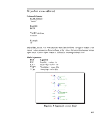
Dependent sources (SPICE E, F, G, H devices)
Standard SPICE formats:
Syntax of the voltage-controlled voltage source
Ename plusout minusout [POLY(k)] n1p n1m
+ [n2p n2m...nkp nkm] p0 [p1...pk] [IC=c1[,c2[,c3...[,ck]]]]
Syntax of the current-controlled current source
Fname plusout minusout [POLY(k)] v1 [v2...vk]
+ p0 [p1...pk] [IC=c1[,c2[,c3...[,ck]]]]
Syntax of the voltage-controlled current source
Gname plusout minusout [POLY(k)]
+n1p n1m [n2p n2m...nkp nkm] p0 [p1...pk]
[IC=c1[,c2[,c3...[,ck]]]]
Syntax of the current-controlled voltage source
Hname plusout minusout [POLY(k)] v1 [v2...vk]
+ p0 [p1...pk] [IC=c1[,c2[,c3...[,ck]]]]
Standard PSpiceTM
supported formats:
Extended syntax of the voltage-controlled voltage source
[E | G]name plusout minusout VALUE = {expression}
[E | G]name plusout minusout TABLE{expression} =
+ input value,output value*
[E | G]name plusout minusout LAPLACE {expression} =
+ {Laplace transfer function}
[E | G]name plusout minusout FREQ
+ {expression} = [KEYWORD]
+frequency value,magnitude value,phase value*
n1p is the first positive controlling node.
n1m is the first negative controlling node.
nkp is the k'th positive controlling node.
nkm is the k'th negative controlling node.
p0 is the first polynomial coefficient.
pk is the k'th polynomial coefficient.
v1 is the voltage source whose current is the first controlling variable.](https://image.slidesharecdn.com/rm102-130625052342-phpapp02/85/Rm10-2-462-320.jpg)
![463
vk is the voltage source whose current is the k'th controlling variable.
c1 is the 1'st initial condition.
ck is the k'th initial condition.
SPICE Examples
E2 7 4 POLY(2) 10 15 20 25 1.0 2.0 10.0 20.0
G2 7 4 POLY(3) 10 15 20 25 30 35 1.0 2.0 3.0 10.0 20.0 30.0
F2 7 4 POLY(2) V1 V2 1.0 2.0 10.0 20.0
H2 7 4 POLY(3) V1 V2 V3 1.0 2.0 3.0 10.0 20.0 30.0
E1 10 20 FREQ {V(1,2)} = (0,0,0) (1K,0,0) (10K,0.001,0)
G1 10 20 TABLE{V(5,6)*V(3)} = (0,0) (1,1) (2,3.5)
E2 10 20 LAPLACE {V(5,6)} = {1/(1+.001*S+1E-8*S*S)}
Schematic format
The schematic attributes are similar to the standard SPICE format without the
plusout and minusout node numbers. The TABLE, VALUE, LAPLACE,
and FREQ features are not supported in the schematic versions of the E, F, G,
and H devices. These features are supported in the Function and Laplace devices,
described later in this chapter.
PART attribute
name
Example
G1
VALUE attribute
[POLY(k)] n1p n1m [n2p n2m...nkp nkm] p0 [p1...pk]
+ [IC=c1[,c2[,c3...[,ck]]]]
[POLY(k)] n1p n1m [n2p n2m...nkp nkm] p0 [p1...pk]
+ [IC=c1[,c2[,c3...[,ck]]]]
[POLY(k)] v1 [v2...vk] p0 [p1...pk] [IC=c1[,c2[,c3...[,ck]]]]
[POLY(k)] v1 [v2...vk] p0 [p1...pk] [IC=c1[,c2[,c3...[,ck]]]]
Examples
POLY(2) 10 15 20 25 1.0 2.0 10.0 20.0
POLY(3) 10 15 20 25 30 35 1.0 2.0 3.0 10.0 20.0 30.0
POLY(2) V1 V2 1.0 2.0 10.0 20.0
POLY(3) V1 V2 V3 1.0 2.0 3.0 10.0 20.0 30.0](https://image.slidesharecdn.com/rm102-130625052342-phpapp02/85/Rm10-2-463-320.jpg)
![467
Diode
SPICE format
Syntax
Dname anode cathode model name [area] [OFF]
+ [IC=vd]
Example
D1 7 8 1N914 1.0 OFF IC=.001
Schematic format
PART attribute
name
Example
D1
VALUE attribute
[area] [OFF] [IC=vd]
Example
10.0 OFF IC=0.65
MODEL attribute
model name
Example
1N914
Both formats
[area] multiplies or divides model parameters as shown in the model parameters
table. The presence of the OFF keyword forces the diode off during the first itera-
tion of the DC operating point. The initial condition, [IC=vd], assigns an initial
voltage to the junction in transient analysis if no operating point is done (or if the
UIC flag is set).
Model statement form
.MODEL model name D ([model parameters])
Example
.MODEL 1N4434 D (IS=1E-16 RS=0.55 TT=5N)](https://image.slidesharecdn.com/rm102-130625052342-phpapp02/85/Rm10-2-467-320.jpg)
![469
Model equations
Figure 22-7 Diode model
Notes and Definitions
The model parameters IS, ISR, IKF, IBV, IBVL, and CJO are multiplied by
[area] and the model parameter RS is divided by [area] prior to their use in the
diode model equations below.
T is the device operating temperature and Tnom is the temperature at which the
model parameters are measured. Both are expressed in degrees Kelvin. T is set
to the analysis temperature from the Analysis Limits dialog box. TNOM is de-
termined by the Global Settings TNOM value, which can be overridden with a
.OPTIONS statement. T and Tnom may both be customized for each model by
specifying the parameters T_MEASURED, T_ABS, T_REL_GLOBAL, and T_
REL_LOCAL. See the .MODEL section of Chapter 26, Command Statements,
for more information on how device operating temperatures and Tnom tempera-
tures are calculated.
Temperature Effects
VT = k • T / q = 1.38E-23 • T / 1.602E-19
IS(T) = IS • e((T/Tnom - 1)•EG/(VT•N))
• (T/Tnom)(XTI/N)
ISR(T) = ISR • e((T/Tnom - 1)•EG/(VT•NR))
• (T/Tnom)(XTI/NR)
IKF(T) = IKF • (1+TIKF•(T - Tnom))
BV(T) = BV • (1+TBV1•(T-Tnom)+TBV2•(T-Tnom)2
)
RS(T) = RS • (1+TRS1•(T-Tnom)+TRS2•(T-Tnom)2
)
VJ(T) = VJ•(T/Tnom)- 3•VT•ln(T/Tnom)- EG(Tnom)•(T/Tnom)+EG(T)
EG(T) = 1.16-.000702•T2
/(T+1108)
EG(Tnom) = 1.17-.000702•Tnom2
/(Tnom+1108)
CJO(T) = CJO•(1+M•(.0004•(T-Tnom) + (1 - VJ(T)/VJ)))](https://image.slidesharecdn.com/rm102-130625052342-phpapp02/85/Rm10-2-469-320.jpg)
![471
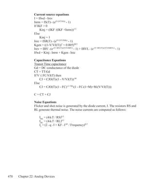
Diode (Philips JUNCAP and JUNCAP2)
SPICE format
Syntax
Dname anode cathode model name
+ AB=diffusion_area
+ LS=nongate_sw_length
+ LG=gate_sw_length
+ MULT=no_parallel
Examples
D1 7 8 MM1 LS=.2u LG=.3u AB=2.4p MULT=50
D2 7 8 MDX LS=11u LG=11u AB=121p MULT=2
Schematic format
PART attribute
name
Example
D1
VALUE attribute
AB=diffusion_area
LS=nongate_sw_length
LG=gate_sw_length
MULT=no_parallel
Example
LS=.46u LG=.12u AB=1.5p MULT=5
MODEL attribute
model name
Example
MM2
Model statement forms
.MODEL model name D (LEVEL=4 [model parameters])
.MODEL model name D (LEVEL=200 [model parameters])](https://image.slidesharecdn.com/rm102-130625052342-phpapp02/85/Rm10-2-471-320.jpg)
![477
Function sources
Schematic format
PART attribute
name
Example
F1
VALUE attribute for formula (NFV and NFI) type
formula
Example of formula type
10*Sin(2*PI*1E6*T)*V(3)*I(L1)*EXP(-V(IN)/100NS)
FREQ attribute
[fexpr]
Example
1200*(1+sqrt(F/1e6))
DERIVATIVE attribute
[Algebraic | Numeric | Default]
Example
Algebraic
NOISE EXPRESSION attribute for NFI only
[noise_expr]
Example
1200*(1+sqrt(F/1e6))
TABLE attribute for table (NTIOFI, NTIOFV, NTVOFV, NTVOFI) types
(x1,y1) (x2,y2) ... ([(xk,yk)])
Curly braces {} are required for expressions and optional for variables.
Examples of table type
(-1m,25) (1m,25) (2m,30)
({start - 1m}, {25*level} ) (end,level) ({end+3m}, level2)](https://image.slidesharecdn.com/rm102-130625052342-phpapp02/85/Rm10-2-477-320.jpg)
![481
GaAsFET
SPICE format
Syntax
Bname drain gate source model name
+ [area] [OFF] [IC=vds[,vgs]]
Example
B1 5 7 9 2N3531 1 OFF IC=1.0,2.5
Schematic format
PART attribute
name
Example
B1
VALUE attribute
[area] [OFF] [IC=vds[,vgs]]
Example
1.5 OFF IC=0.05,1.00
MODEL attribute
model name
Example
GFX_01
The device is an n-channel device. There is no p-channel version. Level 1 speci-
fies the Curtice model, level 2 specifies the Raytheon or Statz model, and level
3 specifies the Triquint model. The [OFF] keyword forces the device off for the
first iteration of the operating point. The initial condition, [IC=vds[,vgs]], assigns
initial voltages to the drain-source and gate-source terms. Additional information
on the model can be found in references (14) and (15).
Model statement form
.MODEL model name GASFET ([model parameters])
Example
.MODEL B1 GASFET (VTO=-2 ALPHA=2 BETA=1E-4 LAMBDA=1E-3)](https://image.slidesharecdn.com/rm102-130625052342-phpapp02/85/Rm10-2-481-320.jpg)
![483
GaAsFET model equations
Figure 22-8 The GaAsFET model
Notes and Definitions
The model parameters BETA, CGS, CGD, and CDS are multiplied by [area] and
the model parameters RG, RD, and RS are divided by [area] prior to their use in
the equations below.
T is the device operating temperature and Tnom is the temperature at which the
model parameters are measured. Both are expressed in degrees Kelvin. T is set
to the analysis temperature from the Analysis Limits dialog box. TNOM is de-
termined by the Global Settings TNOM value, which can be overridden with a
.OPTIONS statement. T and Tnom may both be customized for each model by
specifying the parameters T_MEASURED, T_ABS, T_REL_GLOBAL, and T_
REL_LOCAL. See the .MODEL section of Chapter 26, Command Statements,
for more information on how device operating temperatures and Tnom tempera-
tures are calculated.
Vgs = Internal gate to source voltage
Vds = Internal drain to source voltage
Id = Drain current
VT= k • T / q = 1.38E-23 •T / 1.602E-19
In general, X(T) = Temperature adjusted value of parameter X](https://image.slidesharecdn.com/rm102-130625052342-phpapp02/85/Rm10-2-483-320.jpg)
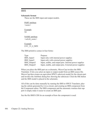
![487
IGBT
SPICE format
Syntax
Zname gate collector emitter model name
+ [AREA=area]
+ [WB=base_width]
+ [AGD=agd]
+ [KP=kp]
+ [TAU=tau]
+ [OFF]
+ [IC=[vgs[,vae[,vds[,veb]]]]]
Example
Z1 1 2 0 IXGH10N170
+ AREA=1E-4 WB=100U AGD=.1N KP=1E-5
+ TAU=100N OFF IC=1,2,3,4
Schematic format
PART attribute
name
Example
Z1
VALUE attribute
[AREA=area] [WB=base_width] [AGD=agd] [KP=kp]
[TAU=tau] [OFF] [IC=[vgs[,vae[,vds[,veb]]]]]
Example
AREA=2E-7 WB=10u
MODEL attribute
model name
Example
IXGH10N170
This device model is based upon the implementation by Gregory Oziemkiewicz
of the IGBT model developed by Allen R. Hefner at the National Institute of
Standards and Technology. The parameter names, default values and units](https://image.slidesharecdn.com/rm102-130625052342-phpapp02/85/Rm10-2-487-320.jpg)
![488 Chapter 22: Analog Devices
are compatible with most SPICE versions of the same model.
The area, base_width, agd, kp, and tau attributes, if specified,
supercede model parameters of the same name.
The [OFF] keyword forces the device off for the first iteration of the operating
point. The initial condition, IC=[vgs[,vae[,vds[,veb]]]], assigns initial voltages to
the model nodes. Additional model information can be found in these references:
Implementation and Development of the NIST IGBT Model in a SPICE-based
Commercial Circuit Simulator, Gregory Todd Oziemkiewicz, Engineer’s Thesis,
University of Florida, December 1995.
Modelling Buffer Layer IGBT’s for Circuit Simulation, Allen R. Hefner Jr, IEEE
Transactions on Power Electronics, Vol. 10, No. 2, March 1995
An Experimentally Verified IGBT Model Implemented in the Saber Circuit
Simulator, Allen R. Hefner, Jr., Daniel M. Diebolt, IEE Transactions on Power
Electronics, Vol. 9, No. 5, September 1994
Model parameters for IGBT model
Name Default Parameter
AGD 5u Gate-drain overlap area
AREA 10u Device area
BVF 1 Avalanche uniformity factor
BVN 4 Avalanche multiplication exponent
CGS 12.4n Gate-source capacitance per unit area
COXD 35n Gate-drain oxide capacitance per unit area
JSNE 650f Emitter saturation current density
KF 1 Triode region factor
KP 380m MOS transconductance
MUN 1.5K Electron mobility
MUP 450 Hole mobility
NB 200T Base doping
T_ABS undefined Absolute temperature
T_MEASURED undefined Parameter measured temperature
T_REL_GLOBAL undefined Relative to current temperature
T_REL_LOCAL undefined Relative to AKO model temperature
TAU 7.1u Ambipolar recombination lifetime
THETA 20m Transverse field factor](https://image.slidesharecdn.com/rm102-130625052342-phpapp02/85/Rm10-2-488-320.jpg)
![492 Chapter 22: Analog Devices
Independent sources (Voltage Source and Current Source)
SPICE format
Syntax for the voltage source
Vname plus minus [[DC ] dcvalue]
+ [AC magval [phaseval]]
+ [PULSE v1 v2 [td [tr [tf [pw [per]]]]]]
OR [SIN vo va [f0 [td [df [ph]]]]]
OR [EXP v1 v2 [td1 [tc1 [td2 [tc2 ]]]]]
OR [PWL t1 v1 t2 v2 ...[tn , vn]]
OR [SFFM vo va f0 [mi [fm]]]
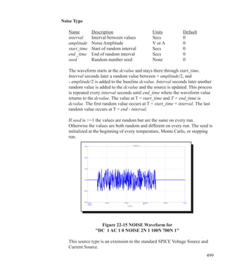
OR [NOISE interval [amplitude [start [end [seed]]]]]
OR [GAUSSIAN amp tpeak width [period]]
Syntax for the current source
The current source syntax is the same as the voltage source except for the
use of I for the first character of the name.
Examples
V3 2 0 DC 0 AC 1 0 SIN 0 1 1MEG 100NS 1E6 0 ;voltage-sin
V5 3 0 DC 0 AC 1 0 EXP 0 1 100N 100N 500N 100N ;voltage-exp
I3 4 0 DC 0 AC 1 0 SFFM 0 1 1E6 .5 1E7 ;current-sffm
V1 5 0 DC 1 AC 1 0 NOISE 10N 1 100N 700N 1 ; voltage-noise
Schematic format
These are the Voltage Source and Current Source components from
Component / Analog Primitives / Waveform Sources.
PART attribute
name
Example
V1
VALUE attribute
value where value is identical to the SPICE format without the name and
the plus and minus node numbers.
Examples
DC 1 PULSE 0 1MA 12ns 8ns 110ns 240ns 500ns
DC 0 AC 1 0 SFFM 0 2 2E6 .5 1E7](https://image.slidesharecdn.com/rm102-130625052342-phpapp02/85/Rm10-2-492-320.jpg)
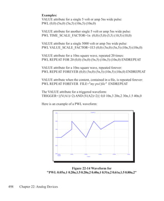
![497
PWL type
General Form:
PWL
+ [TRIGGER={trigger_expression}]
+ [TIME_SCALE_FACTOR=ts_value]
+ [VALUE_SCALE_FACTOR=vs_value]
+(data_pairs OR FILE=filename)
where the syntax of data_pairs is:
tin,in Data pairs must be separated by spaces or commas.
ts_value, if present, multiplies all tin values and vs_value, if present,
multiplies all in values.
Syntax for a single point on the waveform:
(tin,in)
Syntax for m points on the waveform:
(tin1
,in1
) (tin2
,in2
) ... (tinm
,inm
)
Syntax to repeat (data_pairs)* n times:
REPEAT FOR n (data_pairs)* ENDREPEAT
Syntax to repeat (data_pairs)* forever:
REPEAT FOREVER (data_pairs)* ENDREPEAT
Syntax to repeat content of (filename)* n times:
REPEAT FOR n FILE=filename ENDREPEAT
Syntax to repeat content of (filename)* forever:
REPEAT FOREVER FILE=filename ENDREPEAT
The file filename must be a text file and its content must use the same
format as used above in data_pairs.
trigger_expression, if true, enables the waveform or disables it if false.
Each data pair specifies one point on the waveform curve. Intermediate
values are linearly interpolated from the table pairs. There is no specific limit
on the number of data pairs in the table. They may be added indefinitely until
system memory is exhausted.](https://image.slidesharecdn.com/rm102-130625052342-phpapp02/85/Rm10-2-497-320.jpg)
![501
Inductor
SPICE format
Syntax
Lname plus minus [model name]
+ [inductance] [IC=initial current]
Examples
L1 2 3 1U
L2 7 8 110P IC=2
plus and minus are the positive and negative node numbers.
Positive current flows into the plus node and out of the minus node.
Schematic format
PART attribute
name
Example
L1
INDUCTANCE attribute
[inductance] [IC=initial current]
Examples
1U
110U IC=3
1U/(1+I(L2)^2)
FLUX attribute
[flux]
Example
1u*ATAN(I(L2))
FREQ attribute
[fexpr]
Example
1.2mh+5m*(1+log(F))](https://image.slidesharecdn.com/rm102-130625052342-phpapp02/85/Rm10-2-501-320.jpg)
![502 Chapter 22: Analog Devices
MODEL attribute
[model name]
Examples
LMOD
INDUCTANCE attribute
[inductance] may be either a simple number or an expression involving
time-varying variables. Consider the following expression:
1u/(1+I(L2)^2)
I(L2) refers to the value of the L2 current, during a transient analysis, a DC
operating point calculation prior to an AC analysis, or during a DC analysis.
It does not mean the AC small signal L2 current. If the operating point value
for the L2 current was 2 amps, the inductance would be evaluated as
1u/(1+2^2) = 0.2u. The constant value, 0.2u, is then used in AC analysis.
FLUX attribute
[flux], if used, must be an expression involving time-domain variables,
including the current through the inductor and possibly other symbolic
(.define or .param) variables.
Rules about using FLUX and INDUCTANCE expressions
1) Either [inductance] or [flux] must be supplied.
2) If both [inductance] and [flux] are time-varying expressions, the user
must ensure that [inductance] is the derivative of [flux] with respect to the
inductor current.
[inductance] = d([flux])/dI
3) If [inductance] is not given and [flux] is a time-varying expression, MC10
will create an expression for inductance by taking the derivative, L = dX/dI.
4) If [inductance] is a time-varying expression, and [flux] is not given, MC10
will create an equivalent circuit for the inductor consisting of a voltage
source of value L(I)*DDT(I).
5) If [flux] is a time-varying expression, it must involve the current through
the inductor. Even for a constant inductor, X(L) = L*I(L).](https://image.slidesharecdn.com/rm102-130625052342-phpapp02/85/Rm10-2-502-320.jpg)
![503
6) If [inductance] or [flux] is given as a time-varying expression, the
MODEL attribute is ignored and the inductor cannot be referenced by a K
device (mutual inductance). The inductance and flux values are determined
solely by the expressions and are unaffected by model parameters.
Time-varying expression means any expression that uses a variable that can
vary during a simulation run, such as V(L1) or I(L2).
FREQ attribute
If fexpr is used, it replaces the value determined during the operating
point. fexpr may be a simple number or an expression involving frequency
domain variables. The expression is evaluated during AC analysis as the
frequency changes. For example, suppose the fexpr attribute is this:
10mh+I(L1)*(1+1E-9*f)/5m
In this expression, F refers to the AC analysis frequency variable and I(L1)
refers to the AC small signal current through inductor L1. Note that there
is no time-domain equivalent to fexpr. Even if fexpr is present,
[inductance] will be used in transient analysis.
Initial conditions
The initial condition assigns an initial current through the inductor in transient
analysis if no operating point is done (or if the UIC flag is set).
Stepping effects
Both the INDUCTANCE attribute and all of the model parameters may be
stepped. If the inductance is stepped, it replaces [inductance], even if it is an
expression. The stepped value may be further modified by the quadratic and tem-
perature effects.
Quadratic effects
If [model name] is used, [inductance] is multiplied by a factor, QF, which is a
quadratic function of the time-domain current, I, through the inductor.
QF = 1+ IL1•I + IL2•I2
This is intended to provide a subset of the old SPICE 2G POLY keyword, which
is no longer supported.
Temperature effects
The temperature factor is computed as follows:](https://image.slidesharecdn.com/rm102-130625052342-phpapp02/85/Rm10-2-503-320.jpg)
![504 Chapter 22: Analog Devices
If [model name] is used, [inductance] is multiplied by a temperature factor, TF.
TF = 1+TC1•(T-Tnom)+TC2•(T-Tnom)2
TC1 is the linear temperature coefficient and is sometimes given in data sheets as
parts per million per degree C. To convert ppm specs to TC1 divide by 1E6. For
example, a spec of 200 ppm/degree C would produce a TC1 value of 2E-4.
T is the device operating temperature and Tnom is the temperature at which the
nominal inductance was measured. T is set to the analysis temperature from the
Analysis Limits dialog box. TNOM is determined by the Global Settings TNOM
value, which can be overridden with a .OPTIONS statement. T and Tnom may
be changed for each model by specifying values for T_MEASURED, T_ABS,
T_REL_GLOBAL, and T_REL_LOCAL. See the .MODEL section of Chapter
26, Command Statements, for more information on how device operating tem-
peratures and Tnom temperatures are calculated.
Monte Carlo effects
LOT and DEV Monte Carlo tolerances, available only when [model name] is
used, are obtained from the model statement. They are expressed as either a per-
centage or as an absolute value and are available for all of the model parameters
except the T_parameters. Both forms are converted to an equivalent tolerance
percentage and produce their effect by increasing or decreasing the Monte Carlo
factor, MF, which ultimately multiplies the value of the model parameter L.
MF = 1 ± tolerance percentage /100
If tolerance percentage is zero or Monte Carlo is not in use, then the MF factor is
set to 1.0 and has no effect on the final value.
The final inductance, lvalue, is calculated as follows:
lvalue = [inductance] * QF * TF * MF* L, where L is the model parameter
multiplier.
Nonlinear inductor cores and mutual inductance
Use the coupling (K) device to specify a nonlinear magnetic material for the core
using the Jiles-Atherton model.
Model statement form
.MODEL model name IND ([model parameters])](https://image.slidesharecdn.com/rm102-130625052342-phpapp02/85/Rm10-2-504-320.jpg)
![507
JFET
SPICE format
Syntax
Jname drain gate source model name
+ [area] [OFF] [IC=vds[,vgs]]
Example
J1 5 7 9 2N3531 1 OFF IC=1.0,2.5
Schematic format
PART attribute
name
Example
J1
VALUE attribute
[area] [OFF] [IC=vds[,vgs]]
Example
1.5 OFF IC=0.05,1.00
MODEL attribute
model name
Example
JFET_MOD
The value of [area], whose default value is 1, multiplies or divides parameters as
shown in the table. The [OFF] keyword turns the JFET off for the first operating
point iteration. The initial condition, [IC= vds[,vgs]], assigns initial drain-
source and gate-source voltages. Negative VTO implies a depletion mode device
and positive VTO implies an enhancement mode device. This conforms to the
SPICE 2G.6 model. Additional information on the model can be found in refer-
ence (2).
Model statement forms
.MODEL model name NJF ([model parameters])
.MODEL model name PJF ([model parameters])](https://image.slidesharecdn.com/rm102-130625052342-phpapp02/85/Rm10-2-507-320.jpg)
![509
Notes and Definitions
Parameters BETA, CGS, CGD, and IS are multiplied by [area] and parameters
RD and RS are divided by [area] prior to their use in the equations below.
Vgs = Internal gate to source voltage
Vds = Internal drain to source voltage
Id = Drain current
Temperature Dependence
T is the device operating temperature and Tnom is the temperature at which the
model parameters are measured. Both are expressed in degrees Kelvin. T is set
to the analysis temperature from the Analysis Limits dialog box. TNOM is de-
termined by the Global Settings TNOM value, which can be overridden with a
.OPTIONS statement. Both T and Tnom may be customized for each model by
specifying the parameters T_MEASURED, T_ABS, T_REL_GLOBAL, and T_
REL_LOCAL. See the .MODEL section of Chapter 26, Command Statements,
for more information on how device operating temperatures and Tnom tempera-
tures are calculated.
VTO(T) = VTO + VTOTC•(T-Tnom)
BETA(T) = BETA•1.01BETACE•(T-Tnom)
IS(T) = IS•e1.11•(T/Tnom-1)/VT
•(T/Tnom)XTI
EG(T) = 1.16 - .000702•T2
/(T+1108)
PB(T) = PB•( T/Tnom)- 3•VT•ln((T/Tnom))-EG(Tnom)•(T/Tnom)+EG(T)
CGS(T) = CGS•(1+M•(.0004•(T-Tnom) + (1 - PB(T)/PB)))
CGD(T) = CGD•(1+M•(.0004•(T-Tnom) + (1 - PB(T)/PB)))
Current equations
Cutoff Region : Vgs ≤ VTO(T)
Id = 0
Saturation Region : Vds Vgs - VTO(T)
Id=BETA(T)•(Vgs - VTO(T))2
•(1+LAMBDA•Vds)
Linear Region : Vds Vgs - VTO(T)
Id=BETA(T)•Vds•(2•(Vgs - VTO(T))- Vds)•(1+LAMBDA•Vds)](https://image.slidesharecdn.com/rm102-130625052342-phpapp02/85/Rm10-2-509-320.jpg)
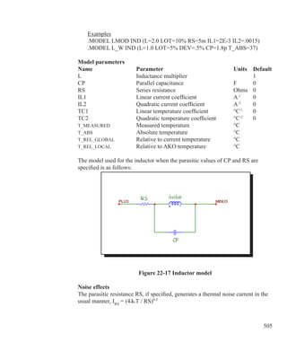
![511
K (Mutual inductance / Nonlinear magnetics model)
SPICE formats
Kname Linductor name Linductor name*
+ coupling value
Kname Linductor name* coupling value
+ model name
Examples
K1 L1 L2 .98
K1 L1 L2 L3 L4 L5 L6 .98
Schematic format
PART attribute
name
Example
K1
INDUCTORS attribute
inductor name inductor name*
Example
L10 L20 L30
COUPLING attribute
coupling value
Example
0.95
MODEL attribute
[model name]
Example
K_3C8
If model name is used, there can be a single inductor name in the INDUC-
TORS attribute. If model name is not used, there must be at least two inductor
names in the INDUCTORS attribute.](https://image.slidesharecdn.com/rm102-130625052342-phpapp02/85/Rm10-2-511-320.jpg)
![514 Chapter 22: Analog Devices
INDUCTORS L1 L2
COUPLING Coupling coefficient between L1 and L2 (0-1.0)
MODEL KCORE
This procedure creates two coupled cores whose magnetic properties are con-
trolled by the KCORE model statement. See the sample circuit file CORE3 for an
example of multiple, coupled core devices.
Model statement form
.MODEL model name CORE ([model parameters ])
Examples
.MODEL K1 CORE (Area=2.54 Path=.54 MS=2E5)
.MODEL K2 CORE (MS=2E5 LOT=25% GAP=.001)
Model parameters
Name Parameter Units Default
Area Mean magnetic cross-section cm2
1.00
Path Mean magnetic path length cm 1.00
Gap Effective air gap length cm 0.00
MS Saturation magnetization a/m 4E5
A Shape parameter a/m 25
C Domain wall flexing constant .001
K Domain wall bending constant 25
Note that the model parameters are a mix of MKS or SI units (a/m) and CGS
units (cm and cm2
).
Model Equations
Definitions and Equations
All calculations are done in MKS (SI) units
µ0
= magnetic permeability of free space = 4*PI*1e-7 Webers/Amp-meter
N= number of turns
Ma = Anhysteretic magnetization
H = Magnetic field intensity inside core
B = Magnetic flux density inside core
M = Magnetization due to domain alignment
I = Core current
V = Core voltage
Ma = MS • H/( |H| +A)
Sign = K if dH/dt 0.0
Sign= - K if dH/dt = 0.0](https://image.slidesharecdn.com/rm102-130625052342-phpapp02/85/Rm10-2-514-320.jpg)
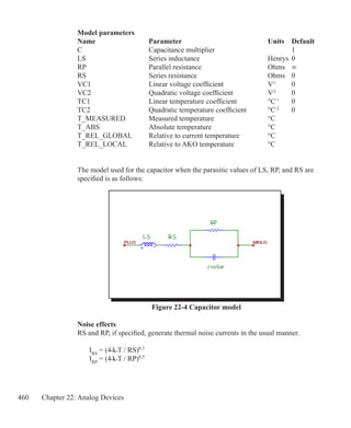
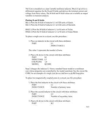
![516 Chapter 22: Analog Devices
Laplace sources
Schematic format
PART attribute
name
Examples
FIL1
LOW1
LAPLACE attribute of LFIOFI, LFIOFV, LFVOFV, LFVOFI
expression
Example
1/(1+.001*S+1E-8*S*S)
FREQ attribute of LTIOFI, LTIOFV, LTVOFV, LTVOFI
(f1,m1,p1) (f2,m2,p2)...(fn,mn,pn)
Example
(0.0,1.0,0.0) (1Meg,0.9,-10) (10Meg,0.2,-35)
KEYWORD attribute (for use with FREQ attribute)
[[DB | MAG] [DEG | RAD]] | [R_I]
Examples
DB RAD
MAG DEG
R_I
There is no SPICE version of this source. Use the Dependent source, E or G de-
vice.
The keywords DB, MAG, DEG, RAD, R_I are interpreted as follows:
DB: Magnitude value is expressed in decibels. (default)
MAG: Magnitude value is true magnitude.
DEG: Degrees value is expressed in degrees. (default)
RAD: Degrees value is expressed in radians.
R_I: The table contains real and imaginary parts.](https://image.slidesharecdn.com/rm102-130625052342-phpapp02/85/Rm10-2-516-320.jpg)
![522 Chapter 22: Analog Devices
MOSFET
SPICE format
Syntax
Mname drain gate source bulk model name
+ [M=mval]
+ [L=length] [W=width] [AD=drainarea] [AS=sourcearea]
+ [PD=drainperiphery] [PS=sourceperiphery]
+ [NRD=drainsquares] [NRS=sourcesquares]
+ [NRG=gatesquares] [NRB=bulksquares]
+ [OFF][IC=vds[,vgs[,vbs]]]
Example
M1 5 7 9 0 IRF350 L=1.5E-6 W=0.25 OFF IC=25.0,8.0
Schematic format
PART attribute
name
Example
M1
VALUE attribute
[M=mval]
+ [L=length] [W=width] [AD=drainarea] [AS=sourcearea]
+ [PD=drainperiphery] [PS=sourceperiphery]
+ [NRD=drainsquares] [NRS=sourcesquares]
+ [NRG=gatesquares] [NRB=bulksquares]
+ [OFF][IC=vds[,vgs[,vbs]]]
Examples
M=20 NRD=10 NRS=25 NRG=5
L=.35u IC=.1, 2.00
L=.4u W=2u OFF IC=0.05,1.00
MODEL attribute
model name
Examples
IRF350
MM150](https://image.slidesharecdn.com/rm102-130625052342-phpapp02/85/Rm10-2-522-320.jpg)
![523
Supported Models
Level Model Name
1 Schichman-Hodges
2 MOS2 Grove-Frohman model (SPICE 3F5)
3 MOS3 empirical model (SPICE 3F5)
4 BSIM1 Original BSIM model (Berkeley Short Channel IGFET)
5 BSIM2 Second generation BSIM model
8, 49 or 53 BSIM3 Third generation BSIM3v3.3 (7/29/2005)
14 or 54 BSIM4 Fourth generation BSIM4.5.0 (7/29/2005)
44 EKV 2.6 Charge based-short channel model developed by the
Swiss Institute of Technology. See the MOSFET(EKV) section
following this MOSFET section
Various Philips MOSFET models. See the Philips MOSFET section
following the EKV section.
width and length are the drawn device dimensions, before side diffusion, in
meters. They can be specified as device attributes, model parameters, or by us-
ing the global default values, DEFW and DEFL. For Levels 1-3, and BSIM 1-3,
DEFNRD and DEFNRS define default drain and source squares, and DEFPD and
DEFPS default drain and source periphery. Device attributes supersede model
parameters, which supersede the global values from the Global Settings dialog
box or a local .OPTIONS statement.
The initialization [IC=vds[,vgs[,vbs]]] assigns initial voltages to the drain-
source, gate-source, and body-source terms in transient analysis if no operating
point is done (or if the UIC flag is set). The [OFF] keyword forces the device off
during the first iteration of the DC operating point.
sourceperiphery and drainperiphery are the diffusion peripheries (m).
sourcearea and drainarea are the diffusion areas (sq. m). Source and drain
junction capacitances may be specified directly by the model parameters CBS
and CBD. If absent, they are calculated from area and periphery terms.
The parasitic resistances may be specified directly with the model parameters
RS, RD, RG, and RB. If unspecified, they are calculated from the product of
the sheet resistivity, RSH, and the number of squares terms, drainsquares,
sourcesquares, gatesquares, and bulksquares. If these terms are absent,
or zero, and the model parameters RS, RD, RG, and RB are absent or zero,
then the parasitic resistances are not included in the model. drainsquares and
sourcesquares default to 0. The other parameter line values also default to
zero.](https://image.slidesharecdn.com/rm102-130625052342-phpapp02/85/Rm10-2-523-320.jpg)
![524 Chapter 22: Analog Devices
mval is a multiplier (default = 1) that provides a way to simulate the effect of
paralleling many devices. It multiplies the effective width, overlap, and junction
capacitances, and the junction currents. It multiplies the drain and source areas,
the device width, and the two peripheries, and divides the four resistances RS,
RD, RG, and RB.
Model statement forms
.MODEL model name NMOS ([model parameters])
.MODEL model name PMOS ([model parameters])
Examples
.MODEL M1 NMOS (W=0.2 L=0.8U KP=1E-6 GAMMA=.65)
.MODEL M2 PMOS (W=0.1 L=0.9U KP=1.2E-6 LAMBDA=1E-3)
Common model parameters
These model parameters are common to levels 1, 2, 3, 4, 5, and 8: Levels 1-5
share common default values. Level 8 defaults are shown in the last column.
Name Parameter Units Default Values For
Lev 1-5 Lev 8
LEVEL Model level 1-5 8
L Channel length m DEFL DEFL
W Channel width m DEFW DEFW
RDS Drain-source shunt resistance Ω ∞ ∞
RD Drain ohmic resistance Ω 0.00 0.00
RS Source ohmic resistance Ω 0.00 0.00
RG Gate ohmic resistance Ω 0.00 0.00
RB Bulk ohmic resistance Ω 0.00 0.00
RSH Source and drain sheet res. Ω/sq 0.00 0.00
CGDO Gate-drain overlap cap. F/m 0.00 0.00
CGSO Gate-source overlap cap. F/m 0.00 0.00
CGBO Gate-bulk overlap cap. F/m 0.00 0.00
CBD Bulk p-n zero-bias B-D cap. F 0.00 0.00
CBS Bulk p-n zero-bias B-S cap. F 0.00 0.00
CJ Bulk p-n zero-bias bot. cap. F/m2
0.00 5E-4
CJSW Bulk p-n zero-bias s/w cap. F/m 0.00 5E-10
MJ Bulk p-n zero-bias bottom grad. 0.50 0.50
MJSW Bulk p-n zero-bias s/w coeff. 0.33 0.33
TT Bulk p-n transit time S 0.00 0.00
IS Bulk p-n saturation current A 1E-14 1E-14
N Bulk p-n emission coefficient 1.00 1.00
JS Bulk p-n bot. current density A/m2
0.00 1E-4](https://image.slidesharecdn.com/rm102-130625052342-phpapp02/85/Rm10-2-524-320.jpg)
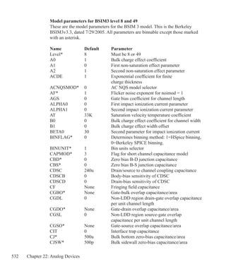
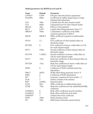
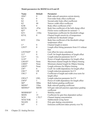
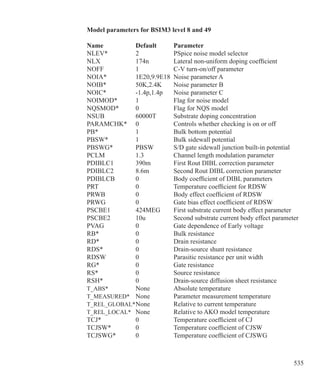
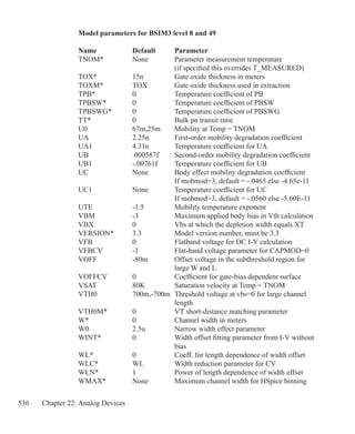
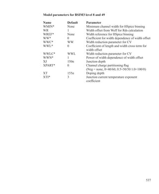
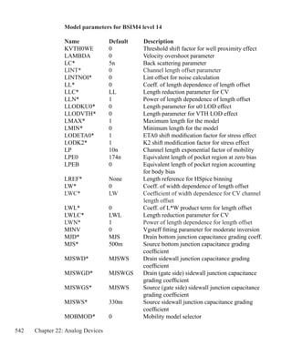
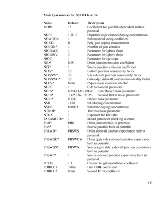
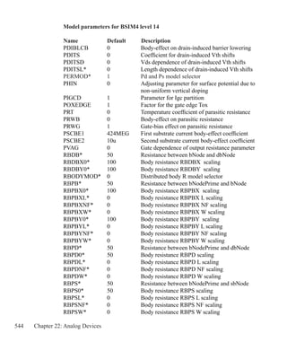
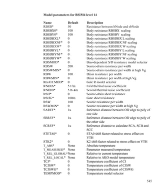
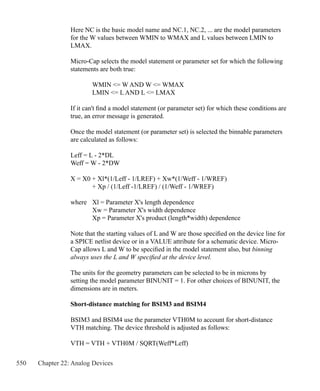
![551
MOSFET (EKV)
SPICE format
The EKV device format is similar to other MOSFETs but has a few more device
parameters that are not found in the other models.
SPICE format
Syntax
Mname drain gate source bulk model name
+ [L=length] [W=width] [AD=drainarea] [AS=sourcearea]
+ [PD=drainperiphery] [PS=sourceperiphery]
+ [NRD=drainsquares] [NRS=sourcesquares]
+ [NRG=gatesquares] [NRB=bulksquares]
+ [NP|M=no_parallel] [NS|N=no_series]
+ [SCALE=scale] [GEO=geometry_model]
+ [TEMP=temperature]
+ [OFF][IC=vds[,vgs[,vbs]]]
Examples of device instance
M1 5 7 9 0 IRF350 L=1.5E-6 W=0.25 NP=10 OFF IC=25.0,8.0
MS 1 2 3 4 NSC SCALE=.8 GEO=2 NRD=1 NRS=2 AS=1E-11 AD=1E-11
Schematic format
PART attribute
name
Example of PART attribute
M1
VALUE attribute
[L=length] [W=width] [AD=drainarea] [AS=sourcearea]
+ [PD=drainperiphery] [PS=sourceperiphery]
+ [NRD=drainsquares] [NRS=sourcesquares]
+ [NRG=gatesquares] [NRB=bulksquares]
+ [NP|M=no_parallel] [NS|N=no_series]
+ [SCALE=scale] [GEO=geometry_model]
+ [TEMP=temperature]
+ [OFF][IC=vds[,vgs[,vbs]]]](https://image.slidesharecdn.com/rm102-130625052342-phpapp02/85/Rm10-2-551-320.jpg)
![552 Chapter 22: Analog Devices
Examples of VALUE attribute
M=20 NRD=10 NRS=25 NRG=5
L=.35u IC=.1, 2.00
L=.4u W=2u OFF IC=0.05,1.00
MODEL attribute
model name
Examples of MODEL attribute
IRF350
width and length are the drawn device dimensions, before side diffusion, in
meters. They can be specified as device attributes, model parameters, or by using
the global default values, DEFW and DEFL. Device attributes supersede model
parameters, which supersede the global DEFW and DEFL values from the Global
Settings dialog box or a local .OPTIONS statement.
The initialization [IC=vds[,vgs[,vbs]]] assigns initial voltages to the drain-
source, gate-source, and body-source terms in transient analysis if no operating
point is done (or if the UIC flag is set). The [OFF] keyword forces the device off
during the first iteration of the DC operating point.
sourceperiphery and drainperiphery are the diffusion peripheries (m).
sourcearea and drainarea are the diffusion areas (sq. m). Source and drain
junction capacitances may be specified directly by the model parameters CBS
and CBD. If absent, they are calculated from area and periphery terms.
The diffusion resistances may be specified directly with the model parameters
RS, RD, RG, and RB. If unspecified, they are calculated from the product of
the sheet resistivity, RSH, and the number of squares terms, drainsquares,
sourcesquares, gatesquares, and bulksquares. If these terms are absent,
or zero, and the model parameters RS, RD, RG, and RB are absent or zero, then
the parasitic resistances are not included in the model. The procedure used to
calculate the resistive values is dependent upon the ACM model parameter and is
described in the section EKV diode parameter calculation methods.
drainsquares and sourcesquares default to 1.0. The other parameter line
values default to zero.
no_parallel is the number of devices in parallel. no_series is the number of
devices in series.](https://image.slidesharecdn.com/rm102-130625052342-phpapp02/85/Rm10-2-552-320.jpg)

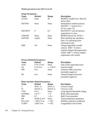
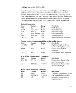

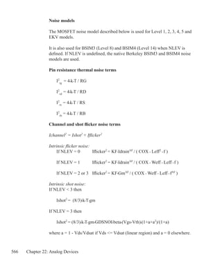
![568 Chapter 22: Analog Devices
MOSFET Philips Model 11
The Philips Model 11 is a compact MOSFET model, intended for digital, analog,
and RF circuit simulation in modern CMOS technologies. Its surface potential
formulation assures continuity of derivatives across operating boundaries. The
instance format is similar to other MOSFET devices but with fewer parameters.
Note that the model includes no source or drain diodes. When needed, these are
added using the JUNCAP diode model, usually as a part of a subcircuit which
includes the MOSFET.
SPICE format
Syntax for Geometrical and Binning models
Mname drain gate source bulk model name
+ [L=length] [W=width] [M=no_parallel]
Syntax for Electrical model
Mname drain gate source bulk model name
+ [M=no_parallel]
Example of device instance for Geometrical and Binning models
MS 1 2 3 4 NSC L=.25u W=1.2u M=20
Schematic format
PART attribute
name
Examples of PART attribute
M1
Syntax for Geometrical and Binning model VALUE attribute
[L=length] [W=width] [M=no_parallel]
Examples of VALUE attribute for Geometrical and Binning models
M=20 L=.4u W=2u
Syntax for Electrical model VALUE attribute
[M=no_parallel]
MODEL attribute
model name](https://image.slidesharecdn.com/rm102-130625052342-phpapp02/85/Rm10-2-568-320.jpg)
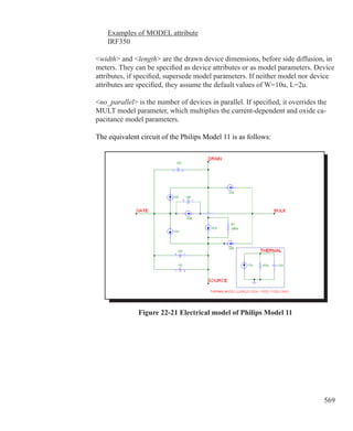
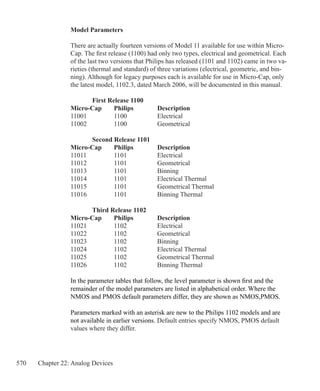
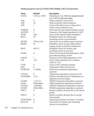
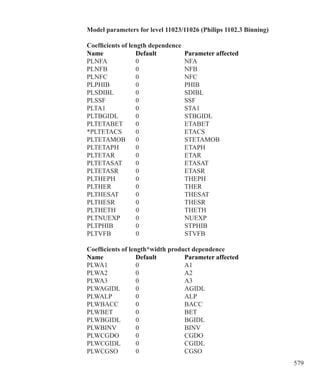
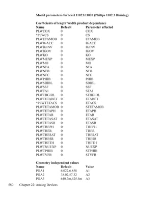
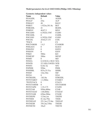
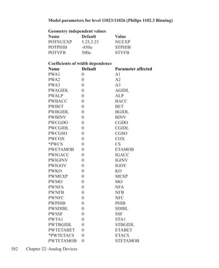
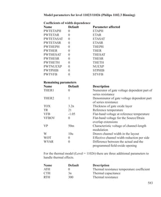
![584 Chapter 22: Analog Devices
MOSFET Philips Model 20
The Philips Model 20 is an asymmetrical, surface-potential-based LDMOS
model, that describes the transition from weak to strong inversion in the channel
region, as well as from accumulation to depletion in the drift region. It provides a
good physical description of effects important for LDMOS devices, such as weak
and strong inversion in the channel region, accumulation and depletion in the
drift region, mobility reduction in both the channel and the drift region, velocity
saturation in the channel region, conductance effects of the channel region (chan-
nel length modulation, DIBL and static feedback), and weak avalanche currents
in the channel region.
Note that the model includes no source or drain diodes. When needed, these are
added using the JUNCAP diode model, usually as a part of a subcircuit which
includes the MOSFET.
SPICE format
Syntax for Electrical model
Mname drain gate source bulk model name
+ [M=no_parallel]
Syntax for Geometrical model
Mname drain gate source bulk model name
+ [W=channel_width] [WD=drift_width] [M=no_parallel]
Example of device instance for Geometrical model
MS 1 2 3 4 NSC W=20u WD=25u M=200
Schematic format
PART attribute
name
Examples of PART attribute
M1
Syntax for Geometrical VALUE attribute
[W=channel_width] [WD=drift_width] [M=no_parallel]
Examples of VALUE attribute for Geometrical model
W=30u WD=15u M=5](https://image.slidesharecdn.com/rm102-130625052342-phpapp02/85/Rm10-2-584-320.jpg)
![585
Syntax for Electrical model VALUE attribute
[M=no_parallel]
MODEL attribute
model name
Examples of MODEL attribute
MODS12
In the Geometrical model, channel_width and drift_width are the drawn
widths of the channel and drift region, before side diffusion, in meters. They can
be specified as device attributes or as model parameters. Device attributes, if
specified, supersede model parameters. If neither model nor device attributes are
specified, they assume the default values of W=20u, WD=20u.
no_parallel is the number of devices in parallel. If specified, it overrides the
MULT model parameter, which multiplies the current-dependent and oxide ca-
pacitance model parameters.
There are two versions of Model 20 available for use within Micro-Cap, the
Electrical and the Geometric. The latest model, dated March 2006, will be docu-
mented here.
Micro-Cap Level Philips Level Description
20011 20.01 MOS20 Electrical
20012 20.01 MOS20 Geometrical
20014 20.01 MOS20 Electrical Thermal
20015 20.01 MOS20 Geometrical Thermal
20021 20.02 MOS20 Electrical
20022 20.02 MOS20 Geometrical
In the table below, the model parameters are listed in alphabetical order.
Parameters marked with an asterisk are new to the Philips 20.02 models and are
not available in the Philips 20.01 models.](https://image.slidesharecdn.com/rm102-130625052342-phpapp02/85/Rm10-2-585-320.jpg)
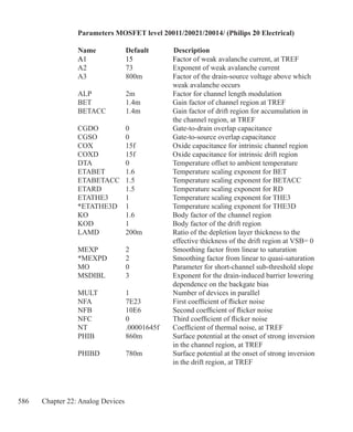
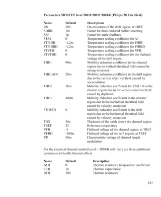
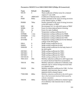
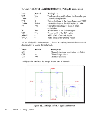
![591
MOSFET Philips Model 31
The Philips Model 31 is a physics based device model suitable for high voltage
applications. The model describes the electrical behavior of a junction isolated
accumulation / depletion MOSFET. The model is used as the drain extension of
high voltage MOS devices, like the Lateral Double-diffused (LDMOS), Vertical
Double-diffused (VDMOS), and Extended MOS transistors.
Note that the model includes no source or drain diodes. When needed, these are
added using the JUNCAP diode model, usually as a part of a subcircuit which
includes the MOSFET.
SPICE format
Syntax
Mname drain gate source bulk model name
+ [M=no_parallel]
Example of device instance
MS 1 2 3 4 NSC M=200
Schematic format
PART attribute
name
Examples of PART attribute
M1
VALUE attribute
[M=no_parallel]
Examples of VALUE attribute
M=5
MODEL attribute
model name
Examples of MODEL attribute
LM1](https://image.slidesharecdn.com/rm102-130625052342-phpapp02/85/Rm10-2-591-320.jpg)
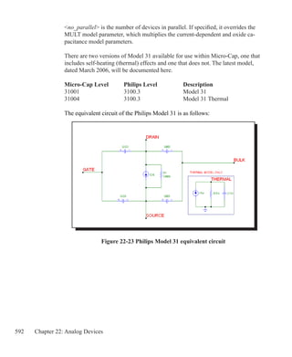
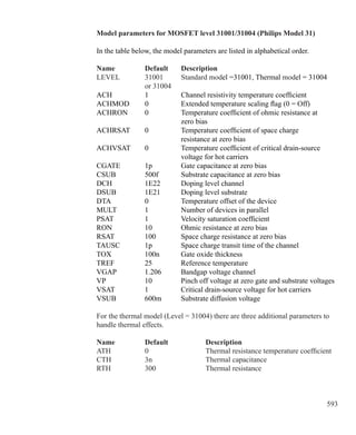
![594 Chapter 22: Analog Devices
MOSFET Philips Model 40
The Philips Model 40 is a physics based model for high voltage applications.
The model describes the electrical behavior of an accumulation / depletion type
MOSFET in Silicon-on-Insulator (SOI) processes. The model is used as a drain
extension of high-voltage MOS devices, like the Lateral Double-diffused MOS
(LDMOS), the Vertical Double-diffused MOS (VDMOS), and the Extended
MOS transistors.
Note that the model includes no source or drain diodes. When needed, these are
added using the JUNCAP diode model, usually as a part of a subcircuit which
includes the MOSFET.
SPICE format
Syntax
Mname drain gate source bulk model name
+ [M=no_parallel]
Example of device instance
MS 1 2 3 4 NSO M=100
Schematic format
PART attribute
name
Example of PART attribute
MS1
VALUE attribute
[M=no_parallel]
Example of VALUE attribute
M=10
MODEL attribute
model name
Example of MODEL attribute
LM1](https://image.slidesharecdn.com/rm102-130625052342-phpapp02/85/Rm10-2-594-320.jpg)
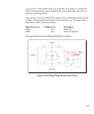
![597
MOSFET PSP Model
The PSP model is a relatively new compact MOSFET model, jointly developed
by Philips Research and Penn State University. It is a surface-potential based
MOS model, describing the key physical effects necessary to model modern
deep-submicron bulk CMOS technologies. These effects include mobility
reduction, velocity saturation, DIBL, gate current, lateral doping gradient effects,
and STI stress. The source/drain junction model, called the JUNCAP2 model, is
an integrated part of the PSP model.
SPICE format
Syntax of electrical model
Mname drain gate source bulk model name
+ [ABSOURCE=bottom_area_source]
+ [ABDRAIN=bottom_area_drain]
+ [LSSOURCE=sti_edge_source] [LSDRAIN=sti_edge_drain]
+ [LGSOURCE=gate_edge_source] [LGDRAIN=gate_edge_drain]
+ [AD=drainarea] [AS=sourcearea]
+ [PD=drainperiphery] [PS=sourceperiphery]
+ [MULT=no_parallel]
+ [JW=jw]
Syntax of geometrical and binning models
Mname drain gate source bulk model name
+ [L=length] [W=width]
+ [SA=source_od-poly_distance] [SB=drain_od-poly_distance]
+ [ABSOURCE=bottom_area_source]
+ [ABDRAIN=bottom_area_drain]
+ [LSSOURCE=sti_edge_source] [LSDRAIN=sti_edge_drain]
+ [LGSOURCE=gate_edge_source] [LGDRAIN=gate_edge_drain]
+ [AD=drainarea] [AS=sourcearea]
+ [PD=drainperiphery] [PS=sourceperiphery]
+ [MULT=no_parallel]
Example of electrical model instance
MS 1 2 3 4 NSO ABSOURCE=2.5p ABDRAIN=3p
Example of geometrical or binning model instance
MS 1 2 3 4 NSO W=.2u L=.09u SA=.12u SB=.12u](https://image.slidesharecdn.com/rm102-130625052342-phpapp02/85/Rm10-2-597-320.jpg)
![598 Chapter 22: Analog Devices
Schematic format
PART attribute
name
Examples of PART attribute
MP1, MX2
Syntax for electrical model VALUE attribute
[ABSOURCE=bottom_area_source]
[ABDRAIN=bottom_area_drain]
[LSSOURCE=sti_edge_source] [LSDRAIN=sti_edge_drain]
[LGSOURCE=gate_edge_source] [LGDRAIN=gate_edge_drain]
[AD=drainarea] [AS=sourcearea]
[PD=drainperiphery] [PS=sourceperiphery]
[MULT=no_parallel]
[JW=jw]
Syntax for geometrical and binning model VALUE attribute
[L=l] [W=w]
[SA=source_od-poly_distance] [SB=drain_od-poly_distance]
[ABSOURCE=bottom_area_source]
[ABDRAIN=bottom_area_drain]
[LSSOURCE=sti_edge_source] [LSDRAIN=sti_edge_drain]
[LGSOURCE=gate_edge_source] [LGDRAIN=gate_edge_drain]
[AD=drainarea] [AS=sourcearea]
[PD=drainperiphery] [PS=sourceperiphery]
[MULT=no_parallel]
Example of VALUE attribute for electrical model
ABSOURCE=5p ABDRAIN=18p LSSOURCE=.2u
Example of VALUE attribute for geometrical or binning model
MULT=10 W=.5u L=.1u SA=.2u SB=.25u
MODEL attribute
model name
Example of MODEL attribute
P102_N
w and l are the drawn device dimensions, before side diffusion, in meters.](https://image.slidesharecdn.com/rm102-130625052342-phpapp02/85/Rm10-2-598-320.jpg)
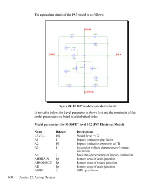
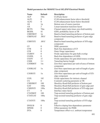
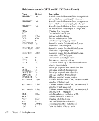
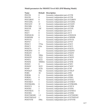
![623
OPAMP
Schematic format
PART attribute
name
Example
OP1
MODEL attribute
model name
Example
LF351
There are three model levels for the OPAMP. Each succeeding level provides
increasingly more realistic models at the expense of increasingly more complex
equivalent circuits.
Level 1 is a simple voltage-controlled current source with a finite output resis-
tance and open loop gain.
Level 2 is a three stage, two pole model with slew rate limiting, finite gain, and
output resistance.
Level 3 is an enhanced Boyle model, similar to those implemented in other
SPICE programs as subcircuits. It is not, however, a macro or a subcircuit, but
a fully internal device model. It models positive and negative slew rates, finite
gain, AC and DC output resistance, input offset voltage and current, phase mar-
gin, common mode rejection, unity gain bandwidth, three types of differential
input, and realistic output voltage and current limiting.
Model statement forms
.MODEL model name OPA ([model parameters])
Examples
.MODEL LM709 OPA (A=45K VOFF=.001 SRP=250K GBW=1E6)
.MODEL LF155 OPA (LEVEL=2 TYPE=1 A=50K SRP=330K)](https://image.slidesharecdn.com/rm102-130625052342-phpapp02/85/Rm10-2-623-320.jpg)
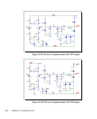
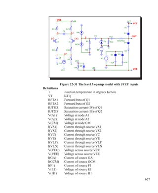
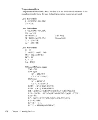
![630 Chapter 22: Analog Devices
Pulse source
Schematic format
PART attribute
name
Example
P1
MODEL attribute
model name
Example
RAMP
The PULSE source is similar to the SPICE PULSE independent voltage source,
except that it uses a model statement and its timing values are defined with re-
spect to T=0.
Model statement forms
.MODEL model name PUL ([model parameters])
Example
.MODEL STEP PUL (VZERO=.5 VONE=4.5 P1=10n P2=20n P3=100n
+ P4=110n P5=500n)
Model parameters
Name Parameter Units Default
VZERO Zero level V 0.0
VONE One level V 5.0
P1 Time delay to leading edge S 1.0E-7
P2 Time delay to one-level S 1.1E-7
P3 Time delay to trailing edge S 5.0E-7
P4 Time delay to zero level S 5.1E-7
P5 Repetition period S 1.0E-6](https://image.slidesharecdn.com/rm102-130625052342-phpapp02/85/Rm10-2-630-320.jpg)
![632 Chapter 22: Analog Devices
Resistor
SPICE format
Syntax
Rname plus minus [model_name]
+resistance [TC=tc1[,tc2]]
Example
R1 2 3 50
plus and minus are the positive and negative node numbers. The
polarity references are used only for plotting or printing the voltage across,
V(RX), and the current through, I(RX), the resistor.
Schematic format
PART attribute
name
Examples
R5
CARBON5
RESISTANCE attribute
resistance [TC=tc1[,tc2]]
Examples
50
10K
50K*(1+V(6)/100)
FREQ attribute
fexpr
Examples
2K+10*(1+F/1e9)
MODEL attribute
[model_name]
Example
RMOD](https://image.slidesharecdn.com/rm102-130625052342-phpapp02/85/Rm10-2-632-320.jpg)
![633
RESISTANCE attribute
resistance may be a constant or an expression involving time-domain
variables. The expression is evaluated in the time domain only. Consider the
expression:
100+V(10)*2
V(10) refers to the value of the voltage on node 10 during a transient
analysis, a DC operating point calculation prior to an AC analysis, or during
a DC analysis. It does not mean the AC small signal voltage on node 10. If
the DC operating point value for node 10 was 2, the resistance would be
evaluated as 100 + 2*2 = 104. The constant value, 104, is used in AC
analysis.
FREQ attribute
If fexpr is used, it replaces the value determined during the operating
point. fexpr may be a simple number or an expression involving frequency
domain variables. The expression is evaluated during AC analysis as the
frequency changes. For example, suppose the fexpr attribute is this:
V(4,5)*(1+F/1e7)
In this expression, F refers to the AC analysis frequency variable and V(4,5)
refers to the AC small signal voltage between nodes 4 and 5. Note that there
is no time-domain equivalent to fexpr. Even if fexpr is present,
resistance will be used in transient analysis.
Stepping effects
The RESISTANCE attribute and all of the model parameters may be stepped. If
it is stepped, it replaces resistance, even if resistance is an expression. The
stepped value may be further modified by the temperature effect.
Temperature effects
There are two different temperature factors, a quadratic factor and an exponential
factor. The quadratic factor is characterized by the model parameters TC1 and
TC2, or tc1 and tc2 from the parameter line. The exponential factor is char-
acterized by the model parameter TCE.
If [TC=tc1[,tc2]] is specified on the parameter line, resistance is multi-
plied by a temperature factor, TF.
TF = 1+tc1•(T-Tnom)+tc2•(T-Tnom)2](https://image.slidesharecdn.com/rm102-130625052342-phpapp02/85/Rm10-2-633-320.jpg)
![634 Chapter 22: Analog Devices
If [model_name] is used and TCE is not specified, resistance is multiplied by a
temperature factor, TF.
TF = 1+TC1•(T-Tnom)+TC2•(T-Tnom)2
TC1 is the linear temperature coefficient and is sometimes given in data sheets as
parts per million per degree C. To convert ppm specs to TC1 divide by 1E6. For
example, a spec of 3000 ppm/degree C would produce a TC1 value of 3E-3.
If [model_name] is used and TCE is specified, value is multiplied by a tem-
perature factor, TF.
TF = 1.01TCE•(T-Tnom)
If both [model_name] and [TC=tc1[,tc2]] are specified, [TC=tc1[,tc2]]
takes precedence.
T is the device operating temperature and Tnom is the temperature at which the
nominal resistance was measured. T is set to the analysis temperature from the
Analysis Limits dialog box. TNOM is determined by the Global Settings TNOM
value, which can be overridden with a .OPTIONS statement. T and Tnom may be
changed for each model by specifying values for T_MEASURED, T_ABS, T_REL_
GLOBAL, and T_REL_LOCAL. See the .MODEL command for more on how de-
vice operating temperatures and Tnom temperatures are calculated.
Monte Carlo effects
LOT and DEV Monte Carlo tolerances, available only when [model_name] is
used, are obtained from the model statement. They are expressed as either a per-
centage or as an absolute value and are available for all of the model parameters
except the T_parameters. Both forms are converted to an equivalent tolerance
percentage and produce their effect by increasing or decreasing the Monte Carlo
factor, MF, which ultimately multiplies the value of the model parameter R.
MF = 1 ± tolerance percentage /100
If tolerance percentage is zero or Monte Carlo is not in use, then the MF factor is
set to 1.0 and has no effect on the final value.
The final resistance, rvalue, is calculated as follows:
rvalue = value * TF * MF * R, where R is the model parameter multiplier.](https://image.slidesharecdn.com/rm102-130625052342-phpapp02/85/Rm10-2-634-320.jpg)
![635
Model statement form
.MODEL model_name RES ([model parameters])
Example
.MODEL RM RES (R=2.0 LOT=10% LS=2.3n TC1=.015)
Model parameters
Name Parameter Units Default
R Resistance multiplier 1.0
LS Series inductance H 0.0
CP Parallel capacitance F 0.0
TC1 Linear temperature coefficient °C-1
0.0
TC2 Quadratic temperature coefficient °C-2
0.0
TCE Exponential temperature coefficient %/°C 0.0
NM Noise multiplier 1.0
T_MEASURED Measured temperature °C
T_ABS Absolute temperature °C
T_REL_GLOBAL Relative to current temperature °C
T_REL_LOCAL Relative to AKO temperature °C
Figure 22-33 Resistor model
Noise effects
Resistor noise is modeled with a thermal noise current:
I = NM * sqrt(4*K*T/rvalue )
NM multiplies the resistor noise current. A value of zero eliminates the noise
contribution from all resistors that use the model.](https://image.slidesharecdn.com/rm102-130625052342-phpapp02/85/Rm10-2-635-320.jpg)
![637
This switch is controlled by the voltage across the two input nodes and the switch
impedance is impressed across the output nodes.
RON and ROFF must be greater than zero and less than 1/Gmin.
Do not make the transition region, VON-VOFF, too small as this will cause an
excessive number of time points required to cross the region. The smallest al-
lowed values for VON-VOFF is (RELTOL•(max(VON,VOFF))+VNTOL).
Model statement forms
.MODEL model name VSWITCH ([model parameters])
Example
.MODEL S1 VSWITCH (RON=1 ROFF=1K VON=1 VOFF=1.5)
.MODEL S2 VSWITCH (RON=1 ROFF=1K VT=3 VH=1)
Model parameters
Name Parameter Units Default
RON On resistance Ohms 1
ROFF Off resistance Ohms 1E6
VON Control voltage for On state V 1
VOFF Control voltage for Off state V 0
VT Threshold voltage V None
VH Hysteresis voltage V None
Model Equations
VC = Voltage across the control nodes
LM = Log-mean of resistor values = ln((RON•ROFF)1/2
)
LR = Log-ratio of resistor values = ln(RON/ROFF)
VM= Mean of control voltages = (VON+VOFF)/2
VD = Difference of control voltages = VON-VOFF
k = Boltzmann's constant
T = Analysis temperature
RS = Switch output resistance](https://image.slidesharecdn.com/rm102-130625052342-phpapp02/85/Rm10-2-637-320.jpg)
![641
Sine source
Schematic format
PART attribute
name
Examples
S1
MODEL attribute
model name
Example
Line60
The Sine source is similar to the SPICE SIN independent voltage source. Unlike
the SPICE source, it uses a model statement.
Model statement form
.MODEL model name SIN ([model parameters])
Example
.MODEL V1 SIN (F=1Meg A=0.6 DC=1.5)
Model parameters
Name Parameter Units Default
F Frequency Hz 1E6
A Amplitude V 1.0
DC DC level V 0.0
PH Phase shift Radians 0.0
RS Source resistance Ω 0.001
RP Repetition period of exponential S 0.00
TAU Exponential time constant S 0.00
Model Equations
If TAU = 0 then
V = A•sin (2•π•F•TIME + PH) + DC
Else
V = A•e(-T/TAU)
•sin (2•π•F•TIME + PH) + DC
where T = TIME mod RP.](https://image.slidesharecdn.com/rm102-130625052342-phpapp02/85/Rm10-2-641-320.jpg)
![643
Subcircuit call
SPICE format
Xname [node]* subcircuit name
+ [PARAMS: parameter name=parameter value*]
+ [TEXT: text name=text value*]
Examples
X1 10 20 AMP
XDIFF 100 200 DIFF PARAMS: GAIN=10
Schematic format
PART attribute
name
Example
X1
NAME attribute
subcircuit name
Example
FILTER
FILE attribute
[file name]
Example
MYFILE.MOD
PARAMS attribute
[parameter name=parameter value*]
Example
CENTER=10kHz BW=1kHz
OPTIONAL attribute
[pin_name=node_name*]
Example
DPWR=$G_DPWR_VCC](https://image.slidesharecdn.com/rm102-130625052342-phpapp02/85/Rm10-2-643-320.jpg)
![644 Chapter 22: Analog Devices
TEXT: attribute
[text name=text value*]
Example
JEDEC=FILENAME
[node]* are the numbers or names of the nodes specified in the .SUBCKT state-
ment. The number of nodes in the subcircuit call must be the same as the number
of nodes in the .SUBCKT statement. When the subcircuit is called, the nodes in
the call are substituted for the nodes in the body of the subcircuit in the same or-
der as they are listed in the .SUBCKT statement.
Any nodes defined in the .SUBCKT statement with the OPTIONAL keyword
may optionally follow the [node]* values. A subset of the optional nodes may be
listed, and will be assigned to the internal subckt nodes in the order specified by
the OPTIONAL statement. If you skip nodes, they must be skipped from the end
of the list. This statement is used in the Digital Library to specify optional power
nodes. Optional nodes can also be specified through the OPTIONAL attribute.
The SPICE subcircuit name or schematic NAME attribute defines the subcir-
cuit name. It must be the same as the name in the defining .SUBCKT statement.
The schematic FILE attribute defines the name of the file in which the .SUBCKT
statement can be found. Micro-Cap looks for the .SUBCKT statement in the fol-
lowing places in the order indicated.
• If the circuit is a schematic:
• In the Text area.
• In the file named in the FILE attribute.
• In one or more files named in a '.LIB' statement.
• In one or more files named in the default '.LIB NOM.LIB' statement.
• If the circuit is a SPICE text file:
• In the circuit description text.
• In one or more files named in a '.LIB' statement.
• In one or more files named in the default '.LIB NOM.LIB' statement.
Subcircuits are used extensively in the Component library. They are accessed via
the default .LIB statement. The SPICE keyword or schematic PARAMS attribute
let you pass multiple numeric parameters to the subcircuit. parameter name is
its name and parameter value defines the value it will assume if the parameter
is not included in the subcircuit call. For example:](https://image.slidesharecdn.com/rm102-130625052342-phpapp02/85/Rm10-2-644-320.jpg)
![646 Chapter 22: Analog Devices
Switch
Schematic format
PART attribute
name
Example
S1
VALUE attribute
[V | T | I],n1,n2 [,ron[,roff]]
Examples
V,1,2
I,2ma,3ma
T,1ms,2ms,50,5Meg
This is the oldest of three types of switches. The newer S and W switches exhibit
a slower, but smoother transition between the off and on states.
There are three types of dependent switches; current-controlled, voltage-con-
trolled, and time-controlled.
The switch is a four-terminal device. A current sensing inductor must be con-
nected across the two input nodes when the current-controlled switch option is
used. Voltage-controlled switches are controlled by the voltage across the two
input nodes. Time dependent switches use the transient analysis time variable to
control the opening and closing of the switch.
The two controlling nodes for a time-controlled switch are not used and may be
shorted to ground or to the two output nodes to reduce the node count by two.
In transient analysis, care must be taken in choosing the time step of the simula-
tion. If the time step is too large, the switch might never turn on. There must be at
least one time point within the specified window for the switch to close or open.
The switch parameter syntax provides for a normally-on or a normally-off switch.
A normally-on switch is one that is on outside the specified window and off in-
side the window. A normally-off switch is one that is off outside the window and
on inside the window.](https://image.slidesharecdn.com/rm102-130625052342-phpapp02/85/Rm10-2-646-320.jpg)

![652 Chapter 22: Analog Devices
Transmission line
SPICE format
Ideal Line
Tname A port + node A port - node
+B port + node B port - node
+[model name]
+ [Z0=value [TD=value] | [F=value [NL=value]]]
Example
T1 10 20 30 40 Z0=50 TD=3.5ns
T1 10 20 30 40 Z0=150 F=125Meg NL=0.5
T1 20 30 40 50 TLMODEL
Lossy Line
Tname A port + node A port - node
+B port + node B port - node
+[model name [physical length]]
+[ LEN=len value R=rvalue L=lvalue G=gvalue
+ C=cvalue]
Examples
T1 20 30 40 50 LEN=1 R=.5 L=.8U C=56PF
T3 1 2 3 4 TMODEL 12.0
Schematic format
PART attribute
name
Example
T1
VALUE attribute for ideal line
Z0=value [TD=value] | [F=value [NL=value]]
Example for ideal line
Z0=50 TD=3.5ns
VALUE attribute for lossy line
physical length LEN=len value R=rvalue L=lvalue
G=gvalue C=cvalue](https://image.slidesharecdn.com/rm102-130625052342-phpapp02/85/Rm10-2-652-320.jpg)
![653
Examples for lossy line
LEN=1 R=.5 L=.8U C=56PF
R=.5 L=.8U C=56PF
MODEL attribute
model name
Example
RELAY
Model statement form
.MODEL model name TRN ([model parameters])
Examples
.MODEL TIDEAL TRN(Z0=50 TD=10ns)
.MODEL TLOSS TRN(C=23pF L=13nH R=.35 LEN=10)
Model parameters for ideal line
Name Parameter Units Default
Z0 Characteristic impedance Ohms None
TD Transmission delay S None
F Frequency for NL Hz None
NL Relative wavelength 0.25
Model parameters for lossy line
Name Parameter Units Default
R Resistance per unit length Ohms / unit None
L Inductance per unit length Henries / unit None
G Conductance per unit length Mhos / unit None
C Capacitance per unit length Farads / unit None
LEN Physical length Same as RLGC None
LEN, R, L, G, and C must use a common unit of length. For example, if C is
measured in units of farads/cm, then R must be in ohms/cm, L must be in henrys/
cm, G must be in mhos/cm, and LEN must be in centimeters.
R, L, C, and G are usually fixed values, but may also be expressions using the
frequency F, or complex frequency S (2*PI*F*j), in AC analysis only. In any
other analysis, expressions are evaluated with F = 0.
Model Equations
The ideal and lossy lines are represented by the model shown in Figure 22-35.](https://image.slidesharecdn.com/rm102-130625052342-phpapp02/85/Rm10-2-653-320.jpg)
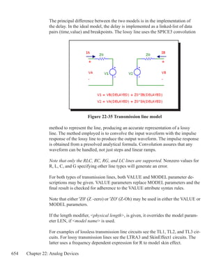
![655
User file source
Schematic format
PART attribute
name
Example
U1
FILE attribute
file name
Example
AMP.USR
EXPRESSION attribute
[expression]
Example
V(OUT) vs T
REPEAT attribute
[number]
Example
5
ENABLE_EXPR attribute
[enable_expression]
Examples
V(OUT)3.2
Time110ns
This is a voltage source whose curve comes from a text file. The curve is repeated
[number] times in transient analysis and once in AC and DC analysis.
The files contain a header and N sequential lines, each with a variable number of
data values:](https://image.slidesharecdn.com/rm102-130625052342-phpapp02/85/Rm10-2-655-320.jpg)
![656 Chapter 22: Analog Devices
Transient analysis:
Two data values per line: Time, Y X set to Time
Three data values per line: Time, X, Y
AC:
Three data values per line: Frequency, Real(Y), Imag(Y) X set to Frequency
Five data values per line: Frequency, Real(X), Imag(X), Real(Y), Imag(Y)
DC: Three data values per line:
DCINPUT1, X, Y
where X is the X expression value, Y is the Y expression value, and
DCINPUT1 is the value of variable1.
User files may be created externally, or by saving one or more curves or wave-
forms after an analysis run. To save a particular waveform, press F10 to invoke
the Plot Properties dialog box after the analysis is over and select the waveform
to be saved from the Save Curves section of the dialog box.
When you place a user source in a schematic, Micro-Cap reads the current data
directory to find any files with the extension *.USR. It then reads the files them-
selves to see what waveforms are available for use. It presents the files and wave-
forms as items in drop-down lists in the FILE and EXPRESSION fields so you
can easily select the file name and waveform expression.
Curves saved in user files can be displayed in an analysis by selecting them from
the Curves section of the Variables list. To invoke this list, click the right mouse
button in the Y Expression field. The X and Y parts of a waveform are stored as
CurveX and CurveY, to let you select the X and Y parts independently.
If [enable_expression] is given, it gates the source. If it is not given, the source
is always enabled. When [enable_expression] is true the waveform starts. If [en-
able_expression] becomes false, the source stays at its current output level.
See USER for an example of a simple source, USER2 for an example of two
sources, and USER3 for an example of a triggered source. Click on Info , then
on the source to examine the data file used by the source.](https://image.slidesharecdn.com/rm102-130625052342-phpapp02/85/Rm10-2-656-320.jpg)
![658 Chapter 22: Analog Devices
vergence problems. In the Hysteresis mode, IT and IH are specified. ION and
IOFF are ignored. The switch impedance changes abruptly from ROFF to RON
as the control current moves past IT+IH and from RON to ROFF as the control
current moves past IT-IH.
This switch is controlled by the current through the source defined by control-
ling voltage source name.
RON and ROFF must be greater than zero and less than 1/Gmin.
Model statement form
.MODEL model name ISWITCH ([model parameters])
Examples
.MODEL W1 ISWITCH (RON=1 ROFF=1K ION=1 IOFF=1.5)
.MODEL W2 ISWITCH (RON=1 ROFF=1K IT=1 IH=1.5)
Model parameters
Name Parameter Units Default
RON On resistance Ohms 1
ROFF Off resistance Ohms 1E6
ION Control current for On state A .001
IOFF Control current for Off state A 0
IT Threshold current A None
IH Hysteresis current A None
Model Equations
IC = Controlling current
LM = Log-mean of resistor values = ln((RON•ROFF)1/2
)
LR = Log-ratio of resistor values = ln(RON/ROFF)
IM = Mean of control currents = (ION+IOFF)/2
ID = Difference of control currents = ION-IOFF
k = Boltzmann's constant
T = Analysis temperature
RS = Switch output resistance](https://image.slidesharecdn.com/rm102-130625052342-phpapp02/85/Rm10-2-658-320.jpg)

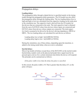
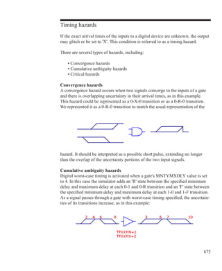
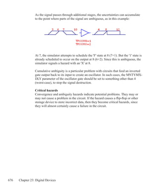
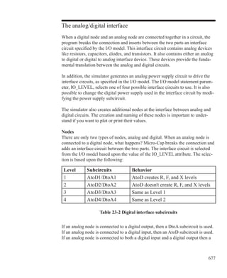
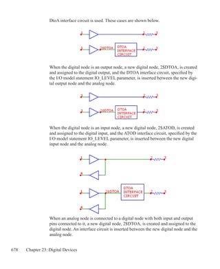
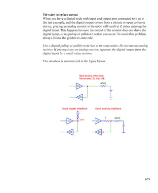
![681
General digital primitive format
The digital device format is similar to the general SPICE component format.
Both analog and digital primitives require node numbers, optional parameters,
and model statements. Analog devices use at most a single model statement. Dig-
ital devices require a timing model statement and an I/O model statement.
Timing model statements define propagation delays and timing constraints. I/O
model statements define the impedances, equivalent circuits, and switching times
of the analog/digital interface model. The I/O model is mainly used when a digi-
tal node is connected to an analog node, but it also defines the impedances used
to resolve states when device outputs of differing strengths are wired together.
Timing model statements embody data unique to each device, so most devices
have unique timing model statements. The same is not true of I/O models since
the interface is generally standardized for all devices within a particular digital
family. For example, all 74LS devices use the same interface specification.
General format
Uname primitive type [(parameter value*)]
+digital power node digital ground node node*
+timing model name I/O model name
+[MNTYMXDLY=delay select value]
+[IO_LEVEL=interface subcircuit select value]
Examples
U1 JKFF(1) $G_DPWR $G_DGND PR CLB CKB J K Q QB D0_74 IO_STD
U1 NOR(3) $G_DPWR $G_DGND 10 20 30 40 D0_74 IO_STD
Definition
Uname
This is the part name.
primitive type
The primitive type specifies which of the primitive digital types, such as
NAND, NOR, JKFF, or PLA, the part is.
[(parameter value*)]
Depending upon the primitive type, these are zero or more parameters repre-
senting the number of input and/or output nodes.](https://image.slidesharecdn.com/rm102-130625052342-phpapp02/85/Rm10-2-681-320.jpg)
![682 Chapter 23: Digital Devices
digital power node digital ground node
These nodes provide power to the A/D interface circuits employed when an ana-
log node is connected to a digital node. Usually the global pins $G_DPWR and
$G_DGND are used. Refer to the section, The analog/digital interface for more
information.
node*
Depending upon the primitive type, these are the node names of the actual input
and/or output node numbers.
timing model name
This name refers to a timing model statement, which specifies propagation and
constraint timing values. Each model has minimum, typical, and maximum val-
ues for each timing parameter. The MNTYMXDLY device parameter selects one
of the values or it lets DIGMNTYMX select one globally.
I/O model name
This name refers to an I/O model statement which specifies impedance and inter-
face circuit information for modeling the analog/digital interface.
[MNTYMXDLY=delay select value]
This value selects the minimum, typical, or maximum value for each timing pa-
rameter as follows:
0=Current value of DIGMNTYMX
1=Minimum
2=Typical
3=Maximum
4=Worst case. Use both minimum and maximum delays.
[IO_LEVEL=interface subcircuit select value]
This selects one of four interface circuits named in the I/O model. These interface
circuits are used at the digital/analog interface. Refer to the I/O model topic at the
end of this chapter for more information.
Timing model form
.MODEL model name model type (model parameters*)
Each primitive type has a unique model type and model parameters.
I/O model form
.MODEL model name UIO (model parameters*)
There is one I/O model structure that is used by all primitives.](https://image.slidesharecdn.com/rm102-130625052342-phpapp02/85/Rm10-2-682-320.jpg)
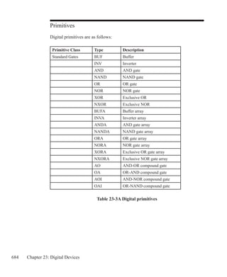
![688 Chapter 23: Digital Devices
Standard gates
SPICE format
Uname gate type[(parameters)*]
+digital power node digital ground node
+input node* output node*
+timing model name I/O model name
+[MNTYMXDLY=delay select value]
+[IO_LEVEL=interface subckt select value]
Examples:
A 5 input NOR gate:
U1 NOR(5) $G_DPWR $G_DGND IN1 IN2 IN3 IN4 IN5 OUT
D0_GATE IO_STD MNTYMXDLY=0 IO_LEVEL=2
A 3 gate NAND array with 2 inputs per gate:
U17 NANDA(2,3) $G_DPWR $G_DGND 1A 1B 2A 2B 3A 3B O1 O2 O3
DLY1 IO_ACT
An AND-OR compound gate having 2 input gates with 3 inputs per gate:
UCMPD AO(3,2) $G_DPWR $G_DGND i1a i1b i1c i2a i2b i2c out
dlymod io_hc_oc MNTYMXDLY=3
Schematic format
PART attribute
name
Example
U1
TIMING MODEL attribute
timing model name
Example
74LS
I/O MODEL attribute
I/O model name
Example
IO_STD](https://image.slidesharecdn.com/rm102-130625052342-phpapp02/85/Rm10-2-688-320.jpg)
![689
MNTYMXDLY attribute
delay select value
Example
2
IO_LEVEL attribute
interface subckt select value
Example
1
POWER NODE attribute
digital power node
Example
$G_DPWR
GROUND NODE attribute
digital ground node
Example
$G_DGND
Model statement form
.MODEL timing model name UGATE ([model parameters])
Example
.MODEL TOR UGATE ( TPLHMN=3ns TPLHTY=5ns TPLHMX=7ns
+ TPHLMN=4ns TPHLTY=6ns TPHLMX=7ns )
The standard gate types and their parameters are shown in Table 23-4. The table
uses the standard syntax:
in one input node
in* one or more input nodes
out one output node
out* one or more output nodes
The phrase # of inputs means the number of inputs per gate. The phrase
# of gates means the number of gates in the array.](https://image.slidesharecdn.com/rm102-130625052342-phpapp02/85/Rm10-2-689-320.jpg)
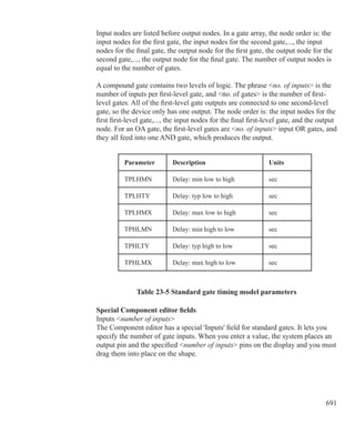
![692 Chapter 23: Digital Devices
Tri-state gates
SPICE format
Uname tri-state gate type[(parameters*)]
+digital power node digital ground node
+input node* enable node output node*
+timing model name I/O model name
+[MNTYMXDLY=delay select value]
+[IO_LEVEL=interface subckt select value]
Examples:
A 3 input tri-state NOR gate:
U20 NOR3(3) $G_DPWR $G_DGND IN1 IN2 IN3 ENABLE OUT
D0_GATE IO_STD MNTYMXDLY=0 IO_LEVEL=2
A 3 gate tri-state AND array with 2 inputs per gate:
UBX AND3A(2,3) $G_DPWR $G_DGND 1A 1B 2A 2B 3A 3B EN O1 O2 O3
DLY1 IO_ACT
Schematic format
PART attribute
name
Example
U1
TIMING MODEL attribute
timing model name
Example
74ALS
I/O MODEL attribute
I/O model name
Example
IO_STD](https://image.slidesharecdn.com/rm102-130625052342-phpapp02/85/Rm10-2-692-320.jpg)
![693
MNTYMXDLY attribute
delay select value
Example
1
IO_LEVEL attribute
interface subckt select value
Example
1
POWER NODE attribute
digital power node
Example
$G_DPWR
GROUND NODE attribute
digital ground node
Example
$G_DGND
Model statement form
.MODEL timing model name UTGATE ([model parameters])
Example
.MODEL TRIG UTGATE ( TPLHMN=2ns TPLHTY=3ns TPLHMX=5ns
+ TPZLMN=4ns TPZLTY=6ns TPZLMX=8ns )
The tri-state gate types and their parameters are shown in Table 23-6. The table
uses the standard syntax:
en one enable node
in one input node
in* one or more input nodes
out one output node
out* one or more output nodes](https://image.slidesharecdn.com/rm102-130625052342-phpapp02/85/Rm10-2-693-320.jpg)
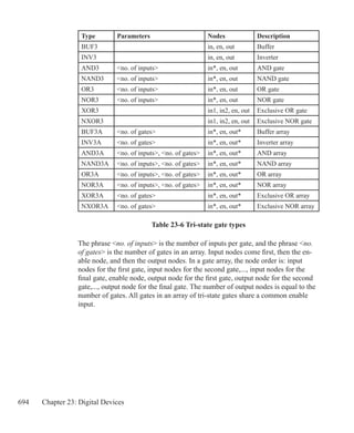
![697
Edge-triggered flip-flops
Two types of edge-triggered flip-flops are provided, the JKFF and the DFF. Both
of these devices change after the active edge of the clock. The active edge of the
JKFF is the negative or falling edge. The active edge of the DFF is the positive or
rising edge.
SPICE format
Uname JKFF(no. of flip-flops)
+digital power node digital ground node
+presetbar node clearbar node clockbar node
+first j node...last j node
+first k node...last k node
+first q node...last q node
+first qbar node...last qbar node
+timing model name I/O model name
+[MNTYMXDLY=delay select value]
+[IO_LEVEL=interface subckt select value]
Uname DFF(no. of flip-flops)
+digital power node digital ground node
+presetbar node clearbar node clock node
+first d node...last d node
+first q node...last q node
+first qbar node...last qbar node
+timing model name I/O model name
+[MNTYMXDLY=delay select value]
+[IO_LEVEL=interface subckt select value]
Examples
U1 JKFF(2) $G_DPWR $G_DGND
+ PREBAR CLRBAR CLKBAR
+J1 J2 K1 K2 Q1 Q2 Q1BAR Q2BAR
+D0_EFF IO_STD IO_LEVEL=1
U4 DFF(1) $G_DPWR $G_DGND
+PREB CLRB CLK
+DIN Q QBAR DLY_DFF IO_ACT](https://image.slidesharecdn.com/rm102-130625052342-phpapp02/85/Rm10-2-697-320.jpg)

![699
Table 23-8a Edge-triggered flip-flop timing model parameters
Model statement form
.MODEL timing model name UEFF ([model parameters])
Example
.MODEL JKDLY UEFF (tppcqlhty=10ns tppcqlhmx=25ns tpclkqlhty=12ns
+twpclty=15ns tsudclkty=4ns)
Parameter Description Units
TPPCQLHMN Delay: min preb/clrb to q/qb low to high sec
TPPCQLHTY Delay: typ preb/clrb to q/qb low to high sec
TPPCQLHMX Delay: max preb/clrb to q/qb low to high sec
TPPCQHLMN Delay: min preb/clrb to q/qb high to low sec
TPPCQHLTY Delay: typ preb/clrb to q/qb high to low sec
TPPCQHLMX Delay: max preb/clrb to q/qb high to low sec
TWPCLMN Width: min preb/clrb low sec
TWPCLTY Width: typ preb/clrb low sec
TWPCLMX Width: max preb/clrb low sec
TPCLKQLHMN Delay: min clk/clkb edge to q/qb low to high sec
TPCLKQLHTY Delay: typ clk/clkb edge to q/qb low to high sec
TPCLKQLHMX Delay: max clk/clkb edge to q/qb low to high sec](https://image.slidesharecdn.com/rm102-130625052342-phpapp02/85/Rm10-2-699-320.jpg)
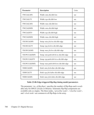
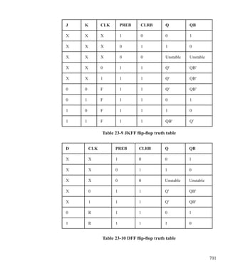
![702 Chapter 23: Digital Devices
Gated latch
Two types of gated latches are provided, the SRFF and the DLTCH. Both devices
change during the high level of the gate.
SPICE format
Uname SRFF(no. of latches)
+digital power node digital ground node
+presetbar node clearbar node gate node
+first s node...last s node
+first r node...last r node
+first q node...last q node
+first qbar node...last qbar node
+timing model name I/O model name
+[MNTYMXDLY=delay select value]
+[IO_LEVEL=interface subckt select value]
Uname DLTCH(no. of latches)
+digital power node digital ground node
+presetbar node clearbar node gate node
+first d node...last d node
+first q node...last q node
+first qbar node...last qbar node
+timing model name I/O model name
+[MNTYMXDLY=delay select value]
+[IO_LEVEL=interface subckt select value]
Examples
U1 SRFF(2) $G_DPWR $G_DGND
+ PREBAR CLRBAR CLK
+S1 S2 R1 R2 Q1 Q2 Q1BAR Q2BAR
+D0_SRFF IO_STD IO_LEVEL=1
U4 DLTCH(1) $G_DPWR $G_DGND
+PREB CLRB GATE
+D1 Q QBAR D_DLTCH IO_ALS](https://image.slidesharecdn.com/rm102-130625052342-phpapp02/85/Rm10-2-702-320.jpg)
![704 Chapter 23: Digital Devices
Table 23-11A Gated latch timing model parameters
Model statement form
.MODEL timing model name UGFF ([model parameters])
Example
.MODEL SR1 UGFF (tppcqlhty=10ns tppcqlhmx=25ns tpgqlhty=12ns
+twpclty=15ns tsudgty=4ns)
Parameter Description Units
TPPCQLHMN Delay: min preb/clrb to q/qb low to high sec
TPPCQLHTY Delay: typ preb/clrb to q/qb low to high sec
TPPCQLHMX Delay: max preb/clrb to q/qb low to high sec
TPPCQHLMN Delay: min preb/clrb to q/qb high to low sec
TPPCQHLTY Delay: typ preb/clrb to q/qb high to low sec
TPPCQHLMX Delay: max preb/clrb to q/qb high to low sec
TWPCLMN Width: min preb/clrb low sec
TWPCLTY Width: typ preb/clrb low sec
TWPCLMX Width: max preb/clrb low sec
TPGQLHMN Delay: min gate to q/qb low to high sec
TPGQLHTY Delay: typ gate to q/qb low to high sec
TPGQLHMX Delay: max gate to q/qb low to high sec
TPGQHLMN Delay: min gate to q/qb high to low sec
TPGQHLTY Delay: typ gate to q/qb high to low sec
TPGQHLMX Delay: max gate to q/qb high to low sec](https://image.slidesharecdn.com/rm102-130625052342-phpapp02/85/Rm10-2-704-320.jpg)
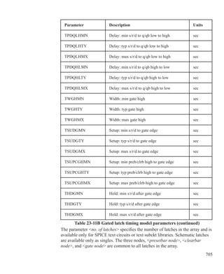
![707
Pullup and pulldown
These devices provide a constant output level at a user-specified strength. The
outputs are as follows:
Device Level Strength
Pullup 1 DRVH (from the I/O model)
Pulldn 0 DRVL (from the I/O model)
These devices provide a strong '1' to pull up or a strong '0' to pull down a group
of open-collector devices whose outputs are wired together.
SPICE format
Uname resistor type(number of resistors)
+digital power node digital ground node
+output node*
+I/O model name
+[IO_LEVEL=interface subckt select value]
resistor type is one of the following:
PULLUP array of digital pullup resistors
PULLDN array of digital pulldown resistors
number of resistors specifies the number of resistors in the array.
Note that these devices are digital devices, not analog devices. Their sole pur-
pose is to provide a strong constant level to a set of open-collector digital devices
whose outputs are wired together. Open-collector devices are simply digital de-
vices with a very large value of DRVH in their I/O model.
PULLUP and PULLDN devices do not use timing models since there is no delay
associated with them. They do, however, need I/O models, since they are digital
devices.
Example
U1 PULLUP(8)
+$G_DPWR $G_DGND
+A1 A2 A3 A4 A5 A6 A7 A8
+ IO_STD](https://image.slidesharecdn.com/rm102-130625052342-phpapp02/85/Rm10-2-707-320.jpg)

![709
Delay line
This device provides a constant delay according to the timing model parameters.
Unlike the other digital devices, there is no inertial cancellation of narrow pulse
widths through delay lines.
SPICE format
Uname DLYLINE
+digital power node digital ground node
+input node output node
+timing model name I/O model name
+[MNTYMXDLY=delay select value]
+[IO_LEVEL=interface subckt select value]
Example
U1 DLYLINE
+$G_DPWR $G_DGND
+IN OUT
+ DMOD IO1
Schematic format
PART attribute
name
Example
U1
TIMING MODEL attribute
timing model name
Example
DELAY1
I/O MODEL attribute
I/O model name
Example
IO_STD
MNTYMXDLY attribute
delay select value](https://image.slidesharecdn.com/rm102-130625052342-phpapp02/85/Rm10-2-709-320.jpg)
![711
Programmable logic arrays
The programmable logic array is designed to allow modeling of a wide variety
of programmable logic devices. The device is constructed of a user-specified
number of inputs, visualized as columns, and a user-specified number of outputs,
which form the rows. Each output (row) is a gate, whose inputs are selected from
the inputs (columns). The device is programmed by choosing the inputs to be
a part of the gate. The type of gate is determined by the PLA type. A PLNAND
provides NAND gates, a PLOR provides OR gates, and so on. The PLA device
provides a programmable core for modeling commercial PLA parts.
There are two ways to program the PLA. The normal way is to provide the data
in a JEDEC format file. These files are normally created as the primary output of
a PLA design program. The second method is to include the data directly in the
SPICE command line or, for schematics, in the DATA attribute.
SPICE format
Uname pld type(no. of inputs,no. of outputs)
+digital power node digital ground node
+input node* output node*
+timing model name I/O model name
+[FILE=file name constant | |file name expression|]
+[DATA=data constant | radix flag$program data$]
+[MNTYMXDLY=delay select value]
+[IO_LEVEL=interface subckt select value]
Schematic format
PART attribute
name
Example
U10
TIMING MODEL attribute
timing model name
Example
PL_04
I/O MODEL attribute
I/O model name](https://image.slidesharecdn.com/rm102-130625052342-phpapp02/85/Rm10-2-711-320.jpg)
![716 Chapter 23: Digital Devices
The data values must be delimited by dollar signs ($). They may be separated by
spaces or placed on continuation lines.
Model statement form
.MODEL timing model name UPLD ([model parameters])
Example
.MODEL PLD1 UPLD (TPLHMN=10ns TPLHTY=25ns TPLHMX=35ns)
Table 23-16 PLA timing model parameters
Parameter Description Default
TPLHMN Delay: min low to high 0
TPLHTY Delay: typ low to high 0
TPLHMX Delay: max low to high 0
TPHLMN Delay: min high to low 0
TPHLTY Delay: typ high to low 0
TPHLMX Delay: max high to low 0
OFFSET
JEDEC file mapping: Address of first input and first
gate program
0
COMPOFFSET
JEDEC file mapping: Address of complement of first
input and first gate program
1
INSCALE
JEDEC file mapping: Amount the JEDEC file address
changes for each new input pin
true only:1
true comp:2
OUTSCALE
JEDEC file mapping: Amount the JEDEC file address
changes for each new output pin (gate)
true only:no. of
inputs
true comp:2*no.
of inputs](https://image.slidesharecdn.com/rm102-130625052342-phpapp02/85/Rm10-2-716-320.jpg)
![717
Multi-bit A/D converter
SPICE format
Uname ADC(bits)
+digital power node digital ground node
+in node ref node gnd node convert node
+status node over-range node
+output msb node output lsb node
+timing model name I/O model name
+[MNTYMXDLY=delay select value]
+[IO_LEVEL=interface subckt select value]
Example
U10 ADC(8) $G_DPWR $G_DGND
+analog_in reference 0 convert status over B7 B6 B5 B4 B3 B2 B1 B0
+IO_STD_OC_ST
Schematic format
PART attribute
name
Example
U10
TIMING MODEL attribute
timing model name
Example
AF_04
I/O MODEL attribute
I/O model name
Example
IO_AC
MNTYMXDLY attribute
delay select value
Example
1](https://image.slidesharecdn.com/rm102-130625052342-phpapp02/85/Rm10-2-717-320.jpg)

![720 Chapter 23: Digital Devices
Model statement form
.MODEL timing model name UADC ([model parameters])
Example
.MODEL A1 UADC (TPCSMN=5ns TPCSTY=15ns TPCSMX=25ns)
Table 23-17 ADC timing model parameters
Parameter Description Units
TPCSMN Delay: min rising edge of Convert to rising edge of Status sec
TPCSTY Delay: typ rising edge of Convert to rising edge of Status sec
TPCSMX Delay: max rising edge of Convert to rising edge of Status sec
TPSDMN Delay: min rising edge of Status to valid data outputs sec
TPSDTY Delay: typ rising edge of Status to valid data outputs sec
TPSDMX Delay: max rising edge of Status to valid data outputs sec
TPDSMN Delay: min data outputs valid to falling edge of Status sec
TPDSTY Delay: typ data outputs valid to falling edge of Status sec
TPDSMX Delay: max data outputs valid to falling edge of Status sec
See the sample circuit AD16 for an example of the use of this type of device.](https://image.slidesharecdn.com/rm102-130625052342-phpapp02/85/Rm10-2-720-320.jpg)
![721
Multi-bit D/A converter
SPICE format
Uname DAC(no. of bits)
+digital power node digital ground node
+out node ref node gnd node
+input msb node input lsb node
+timing model name I/O model name
+[MNTYMXDLY=delay select value]
+[IO_LEVEL=interface subckt select value]
Example
U10 DAC(8) $G_DPWR $G_DGND
+analog_out reference 0 B7 B6 B5 B4 B3 B2 B1 B0
+ D0_EFF IO_STD_ST
Schematic format
PART attribute
name
Example
U10
TIMING MODEL attribute
timing model name
Example
DACTM
I/O MODEL attribute
I/O model name
Example
IO_HCT
MNTYMXDLY attribute
delay select value
Example
1](https://image.slidesharecdn.com/rm102-130625052342-phpapp02/85/Rm10-2-721-320.jpg)
![723
Binary inputs in the 'X' state translate to analog voltages halfway between the
analog voltage for the '0' state and the '1' state.
Following a change on one or more of the binary inputs, the analog output
changes linearly from the old state to the new state over the specified TSW time
as shown in the timing diagram below.
Figure 23-3 DAC timing diagram
See the sample circuit AD16 for an example of the use of this type of device.
Model statement form
.MODEL timing model name UDAC ([model parameters])
Example
.MODEL DAC1 UDAC (TSWMN=5ns TSWTY=15ns TSWMX=25ns)
Parameter Description Units
TSWMN Switching time: min data change to stable analog out sec
TSWTY Switching time: typ data change to stable analog out sec
TSWMX Switching time: max data change to stable analog out sec
Table 23-18 DAC timing model parameters](https://image.slidesharecdn.com/rm102-130625052342-phpapp02/85/Rm10-2-723-320.jpg)
![725
Logic expression
The logic expression primitive provides a means for describing complex digital
behavior. It lets you define the behavior of outputs with standard Boolean alge-
bra, using as variables, input states, temporary states, and output states.
SPICE format
Uname LOGICEXP(no. of inputs,no. of outputs)
+digital power node digital ground node
+first input node...last input node
+first output node...last output node
+timing model name
+I/O model name
+[MNTYMXDLY=delay select value]
+[IO_LEVEL=interface subckt select value]
+ LOGIC:logic assignments*
Schematic format
Logic expressions are usually found in the text file libraries. They are not often
used directly as schematic components, although they can be. For this reason,
only a few sample logic expression components are included in the Component
library.
PART attribute
name
Example
U10
TIMING MODEL attribute
timing model name
Example
DLOGIC
I/O MODEL attribute
I/O model name
Example
IO_STD](https://image.slidesharecdn.com/rm102-130625052342-phpapp02/85/Rm10-2-725-320.jpg)
![728 Chapter 23: Digital Devices
Logic expression operators and their precedence are as follows:
Operator Definition Precedence
~ Unary negation 1
AND 2
^ Exclusive OR 3
| OR 4
Operands are one of the following:
input nodes
Previously assigned temporary values
Previously assigned output nodes
Constants: '0, '1, 'R, 'F, and 'X. Note that the mandatory single quote (') is a
part of the constant name.
Parentheses may be freely used to group expressions.
Timing model format
The timing model is identical to the standard gate primitive UGATE format:
.MODEL timing model name UGATE ([model parameters])
Simulation behavior
The LOGIC statement is evaluated when any input or output pin changes state.
Each logic assignment is evaluated in the order listed within the LOGIC
statement. Expressions have no delay. Any output node name that changes is
scheduled with the appropriate delay from the timing model. Note that usually
the timing model delays are set to zero. Instead, delay is modeled by having the
outputs drive the inputs of a pin-to-pin delay device. These devices provide logi-
cal control of delay based upon inputs that make implementing data sheet delays
easy. Internal feedback is forbidden. This means a logic assignment should
only use previously assigned temporary values or output nodes.
Table 23-19 Logic expression operators](https://image.slidesharecdn.com/rm102-130625052342-phpapp02/85/Rm10-2-728-320.jpg)
![730 Chapter 23: Digital Devices
Pin-to-pin delay
The PINDLY primitive provides a way of modeling complex conditional pin
delays. Conceptually, it can be pictured as a set of channels, where the delay
through each is controlled by a set of user-defined rules. Rules assign a delay to a
particular channel based upon activity at the pins. A typical rule might say:
OUT1 = {CHANGED(REF1,0) TRN_LH, DELAY(10NS,15NS,18NS)}
This means, If the REF1 pin changed in the last 0 seconds, and the channel node
OUT1 is making a low to high transition, then the delay for the OUT1 channel is
min=10ns, typ=15ns, max=18ns.
PINDLY primitives are typically used within a subckt between the logic expres-
sion outputs and the subckt outputs. That is, the inputs to a PINDLY are usually
the outputs of a logic expression. The outputs of a PINDLY are usually the out-
puts of the subcircuit which embodies the full digital model of the part.
A PINDLY may use multiple conditional rules to determine the delay on each
channel. Reference and enable pin states may be used in the rule logic.
SPICE format
Uname PINDLY(no. of paths,no. of enables,no. of refs)
+digital power node digital ground node
+first input node...last input node
+first enable node...last enable node
+first reference node...last reference node
+first output node...last output node
+I/O model name
+[MNTYMXDLY=delay select value]
+[IO_LEVEL=interface subckt select value]
+[BOOLEAN:boolean assignments*]
+[PINDLY:delay assignments*]
+[TRISTATE: ENABLE LO | HI enable node delay assignments*]
+[SETUP_HOLD:setup_hold specifications]
+[WIDTH:width specifications]
+[FREQ:freq specifications]
+[GENERAL:general specifications]](https://image.slidesharecdn.com/rm102-130625052342-phpapp02/85/Rm10-2-730-320.jpg)
![731
Schematic format
PINDLYs are most commonly found in the text file libraries. They are not often
used directly as schematic components, although they can be. For this reason,
only a few token PINDLY components are found in the Component library.
PART attribute
name
Example
P20
PINDELAY attribute
[BOOLEAN:boolean assignments*]
+[PINDLY:delay assignments*]
+[TRISTATE: ENABLE LO | HI enable node delay assignments*]
This attribute is a full PINDELAY statement or, more commonly, the name of a
PINDELAY statement defined with a .define statement in the text area or in a file
referenced by a .lib statement in the schematic.
Examples
CARRY_DELAYS ; defined with a .define statement in the text area
PINDLY: OUT1= {(DELAY (10NS,20NS,30NS))}
PINDLY: BIT2= {CASE (CHANGED(REF1,O),DELAY (10NS,20NS,30NS))}
BOOLEAN:
+READY={CHANGED_LH(GATE,0)}
+LOW={CHANGED_LH(SEC,0)}
+PINDLY: BIT2 = { CASE (READY LOW),
+ DELAY (10NS,20NS,30NS)) }
I/O MODEL attribute
I/O model name
Example
IO_STD
MNTYMXDLY attribute
delay select value](https://image.slidesharecdn.com/rm102-130625052342-phpapp02/85/Rm10-2-731-320.jpg)
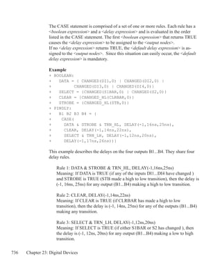
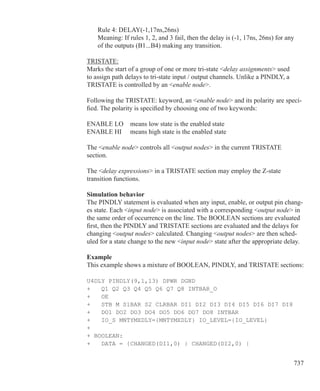
![739
Constraint checker
The CONSTRAINT primitive provides a way of checking complex conditional
timing parameters. It lets you check setup and hold time, pulse width and fre-
quency, and includes a general user-defined check to model unique requirements.
Constraints usually accept as inputs the part or subcircuit inputs and typically
work in concert with logic expressions, pin-to-pin delays, and other digital primi-
tives. Constraints are passive warning devices. They create timing violation mes-
sages and place them in the Numeric Output window. They normally do not af-
fect simulation results. The I/O model attribute is required only to handle the case
of an accidental connection of a Constraint digital node to an analog node.
SPICE format
Uname CONSTRAINT(no. of inputs)
+digital power node digital ground node
+first digital input node...last digital input node
+I/O model name
+[IO_LEVEL=interface subckt select value]
+[BOOLEAN:boolean assignments]
+[SETUP_HOLD:setup_hold specifications]
+[WIDTH:width specifications]
+[FREQ:freq specifications]
+[GENERAL:general specifications]
Schematic format
Constraints are usually found in the text file libraries. They aren't often used di-
rectly as schematic components, although they can be. For this reason, only a few
sample constraint components are to be found in the Component library.
PART attribute
name
Example
C20
CONSTRAINT attribute
[BOOLEAN:boolean assignments]
+[SETUP_HOLD:setup_hold specifications]
+[WIDTH:width specifications]
+[FREQ:freq specifications]
+[GENERAL:general specifications]](https://image.slidesharecdn.com/rm102-130625052342-phpapp02/85/Rm10-2-739-320.jpg)
![741
requires the input pin placements, including all possible constraint devices in the
library is not feasible. Only a few such devices are to be found in the library, and
they are mainly for illustration. These devices are really targeted for use in text
file subcircuits. While you can use them directly in schematics, their real power
issues from their use in the models of commercial digital parts.
Format definitions
BOOLEAN:
Marks the start of a group of one or more boolean assignments used as tempo-
rary variables in subsequent specifications. A boolean assignment is of the
following form:
boolean variable = {boolean expression}
boolean expression
This is the same as in the PINDLY, with the singular exception that the transition
functions (TRN_pc) are not available.
SETUP_HOLD:
Marks the start of a setup_hold specification. The format is as follows:
+SETUP_HOLD:
+CLOCK assertion edge = input node
+DATA(no. of data inputs) = first input node...last input node
+[SETUPTIME=time value]
+[HOLDTIME=time value]
+[WHEN=boolean expression]
+[MESSAGE=extra message text]
+[ERRORLIMIT=limit value]
The CLOCK argument input node defines the input node that serves as a
reference for the setup/hold specification. The CLOCK assertion edge is one
of the following:
LH This specifies that the clock low to high edge is the assertion edge.
HL This specifies that the clock high to low edge is the assertion edge.
The DATA arguments first input node...last input node specify one or more
input nodes whose setup or hold time is to be measured. There must be at least
one input node. The arguments must be separated by a space or a comma.
The SETUPTIME argument time value specifies the minimum time that all](https://image.slidesharecdn.com/rm102-130625052342-phpapp02/85/Rm10-2-741-320.jpg)
![743
If either the CLOCK node or the DATA node are unknown, the check is skipped
to avoid the profusion of errors that usually result. If a clock is X when DATA
changes or vice-versa, the error has probably already been flagged elsewhere.
The constraint is checked only if boolean expression is true. If the number of
constraint warning messages exceeds limit value, no further messages are is-
sued. extra message text if any, is added to the standard error message.
WIDTH:
Marks the start of a group of one or more width specifications which have the
following format:
+WIDTH:
+NODE=input node
+[MIN_LO=time value]
+[MIN_HI=time value]
+[WHEN=boolean expression]
+[MESSAGE=extra message text]
+[ERRORLIMIT=limit value]
The NODE argument, input node, defines the node whose input is to be
checked for width.
The MIN_LO argument, time value, defines the minimum time that input
node can be at the 0 level. If time value is specified as zero, the width check
is not performed.
The MIN_HI argument, time value, defines the minimum time that input
node can be at the 1 level. If time value is specified as zero, the width check
is not performed.
At least one of the two forms, MIN_LO or MIN_HI must be present inside every
WIDTH specification.
The constraint is checked only if boolean expression is true. If the number of
constraint warning messages exceeds limit value, no further messages are is-
sued. extra message text if any, is added to the standard error message.
FREQ:
Marks the start of a group of one or more freq specifications which have the
following format:](https://image.slidesharecdn.com/rm102-130625052342-phpapp02/85/Rm10-2-743-320.jpg)
![744 Chapter 23: Digital Devices
+FREQ:
+NODE = input node
+[MINFREQ=freq value]
+[MAXFREQ=freq value]
+[WHEN=boolean expression]
+[MESSAGE=extra message text]
+[ERRORLIMIT=limit value]
The NODE argument, input node, defines the node whose input is to be
checked for frequency.
The MINFREQ argument, freq value, defines the minimum permissible fre-
quency on input node.
The MAXFREQ argument, freq value, defines the maximum permissible fre-
quency on input node.
Either MINFREQ or MAXFREQ must be present in every FREQ specification.
How it works
FREQ checks compare the frequency on input node with freq value. If the
frequency is greater than MAXFREQ or less than MINFREQ, the appropriate
error message is issued.
WIDTH checks compare the low and high pulse widths on input node with
time value. If the high pulse width is less than MIN_HI or the low pulse width
is less than MIN_LO, the appropriate error message is issued.
WIDTH and FREQ checks are identical if the pulse duty cycle is exactly 50%.
Otherwise, the WIDTH check is somewhat more flexible, as it allows for the pos-
sibility of asymmetric duty cycles.
The constraint is checked only if boolean expression is true. If the number of
constraint warning messages exceeds limit value, no further messages are is-
sued. extra message text if any, is added to the standard error message.
GENERAL:
Marks the start of a group of one or more general specifications which have
the following format:](https://image.slidesharecdn.com/rm102-130625052342-phpapp02/85/Rm10-2-744-320.jpg)

![747
Stimulus devices
Digital networks usually require stimulus devices for testing and simulation.
These devices create a temporal sequence of digital states to stimulate the circuit.
They are the digital equivalent of the analog sources, SIN, PULSE, USER, Volt-
age Source, and Current Source.
There are two types of sources. The stimulus generator (STIM), and the file stim-
ulus (FSTIM). The STIM device uses a language of basic commands to create
virtually any waveform. The FSTIM device reads its waveforms from an external
file.
There is no timing model, since timing information is an inherent property of the
stimulus devices.
Stimulus generator
The stimulus generator primitive provides a flexible language of commands for
creating highly complex digital waveforms. Its format is as follows:
SPICE format
Uname STIM(width,format array)
+digital power node digital ground node node*
+I/O model name] [IO_LEVEL=interface subckt select value]
+[TIMESTEP=stepsize] commands*
Schematic format
PART attribute
name
Example
C20
FORMAT attribute
format array
Example
1111 ; four binary values](https://image.slidesharecdn.com/rm102-130625052342-phpapp02/85/Rm10-2-747-320.jpg)
![748 Chapter 23: Digital Devices
COMMAND attribute
command_name
Example
BINARY16
I/O MODEL attribute
I/O model name
Example
IO_STD
TIMESTEP attribute
[stepsize]
Example
10ns
IO_LEVEL attribute
interface subckt select value
Example
0
POWER NODE attribute
digital power node
Example
$G_DPWR
GROUND NODE attribute
digital ground node
Example
$G_DGND
Definitions
width
In a SPICE file, this is the number of signals or output nodes. For a schematic
part, width is set when the part is entered in the Component library, so simply
picking a STIM device from the library menu supplies this information.](https://image.slidesharecdn.com/rm102-130625052342-phpapp02/85/Rm10-2-748-320.jpg)
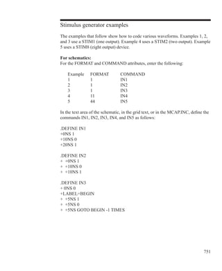
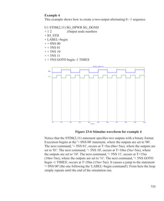
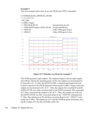
![757
The File Stimulus device
The File Stimulus device lets you import digital waveforms from a text file. This
device lets you import digital waveforms from other simulators or from the Mi-
cro-Cap output file (with some editing).
File Stimulus input file format
The File Stimulus device expects to read a file in the following format:
Header
One or more blank lines
Transition tables
Header
This consists of the following:
[TIMESCALE=time scale value]
[first signal name...last signal name]
OCT(signal name bit 3...signal name of lsb)...
HEX(signal name bit 4...signal name of lsb)...
Header contains the optional [TIMESCALE=value] line and a single line
list of signal names. The signal names may be separated by spaces, commas, or
tabs. The line may not be continued with the continuation character '+'. The line
may contain up to 256 signals. The signal names will be associated with signal
values from the Transition tables, in the same order.
The optional OCT(sig3, sig2, sig1) radix function lets you declare seg-
ments of the transition table as octal numbers. It decodes each octal digit from the
table into three binary values and assigns these values to the three signal names.
The function must have exactly three signal names as arguments and it consumes
one octal digit from each row in the transition table.
The optional HEX(sig4, sig3, sig2, sig1) radix function lets you de-
clare segments of the transition table as hex numbers. It decodes each hex digit
into four binary values and assigns the values to the four signal names. The func-
tion must have exactly four signal names as arguments and it consumes one hex
digit from each row in the transition table.](https://image.slidesharecdn.com/rm102-130625052342-phpapp02/85/Rm10-2-757-320.jpg)
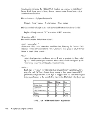
![759
Transition Table example
TIMESCALE=1NS
A B C D HEX(A4,A3,A2,A1) OCT(D3,D2,D1)
0 0000F3 ; transition time =0
1 000104 ; transition time =1NS
+2 001015 ; transition time =3NS (1NS+2NS)
5 001126 ; transition time =5NS
SPICE format
Uname FSTIM(no. of outputs)
+digital power node digital ground node
+node*
+I/O model name
+ FILE=stimulus file name
+[IO_LEVEL=interface subckt select value]
+[SIGNAMES=signal names from stimulus file]
Schematic format
PART attribute
name
Example
FS1
I/O MODEL attribute
I/O model name
Example
IO_STD
FILE attribute
file_name
Example
MYFILE.STM
REPEAT attribute
count
Example
1](https://image.slidesharecdn.com/rm102-130625052342-phpapp02/85/Rm10-2-759-320.jpg)
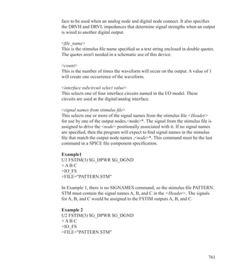
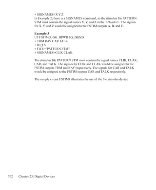
![763
I/O model
I/O models provide the information necessary to determine the output strength
when devices are wire-ored together, and to create the interface circuits when the
digital part is connected to an analog part.
I/O models capture the electrical information common to the IC technology and
circuit techniques used to design and build them. Thus, a typical digital family
will have only four or five I/O models. The only difference in the I/O models
within a digital family is to account for the different circuits employed at the
input or output, as, for example, in open-collector outputs and Schmitt-trigger
inputs.
I/O model format
.MODEL I/O model name UIO ([model parameters])
Parameter Description Units Default
INLD Input load capacitance farad 0
OUTLD Output load capacitance farad 0
DRVH Output high level resistance ohm 50
DRVL Output low level resistance ohm 50
DRVZ Output Z state resistance ohm 250K
INR Input leakage resistance ohm 30K
TSTOREMN Min storage time for charge storage node sec 1E-3
AtoD1 AtoD interface circuit for level 1 AtoDDefault
DtoA1 DtoA interface circuit for level 1 DtoADefault
AtoD2 AtoD interface circuit for level 2 AtoDDefault
DtoA2 DtoA interface circuit for level 2 DtoADefault
Table 23-22 I/O model parameters](https://image.slidesharecdn.com/rm102-130625052342-phpapp02/85/Rm10-2-763-320.jpg)

![766 Chapter 23: Digital Devices
Digital / analog interface devices
When a digital node and an analog node are connected together in a circuit, the
system breaks the connections and inserts between the two parts the interface
circuit specified in the I/O model. These interface circuits contain analog devices
like resistors, capacitors, diodes, and transistors. They also contain either an ana-
log to digital or digital to analog interface device. These devices provide the fun-
damental translation between the analog and digital circuits.
Digital input device (N device)
When a digital output node is connected to an analog node, the interface circuit
requires an N device. Its function is to translate digital levels to analog voltages
and impedances to drive the analog node.
SPICE format
Nname interface node low level node high level node
+model name
+ DGTLNET=digital node name
+I/O model name
+[IS=initial state]
Schematic format
PART attribute
name
Example
FS1
MODEL attribute
model name
Example
D0_AD
I/O MODEL attribute
I/O model name
Example
IO_STD](https://image.slidesharecdn.com/rm102-130625052342-phpapp02/85/Rm10-2-766-320.jpg)
![767
IS attribute
initial state
Example
1
Model form
.MODEL model name DINPUT ([model parameters])
Parameter Description Units Default
CLO Capacitance to low level node farad 0
CHI Capacitance to high level node farad 0
S0NAME State '0' character abbreviation
S0TSW State '0' switching time sec
S0RLO State '0' resistance to low level node ohm
S0RHI State '0' resistance to high level node ohm
S1NAME State '1' character abbreviation
S1TSW State '1' switching time sec
S1RLO State '1' resistance to low level node ohm
S1RHI State '1' resistance to high level node ohm
.
.
.
.
.
.
S19NAME State '19' character abbreviation
S19TSW State '19' switching time sec
S19RLO State '19' resistance to low level node ohm
S19RHI State '19' resistance to high level node ohm
Table 23-23 The N device model parameters](https://image.slidesharecdn.com/rm102-130625052342-phpapp02/85/Rm10-2-767-320.jpg)

![770 Chapter 23: Digital Devices
Digital output device (O device)
When a digital input node is connected to an analog node, the A/D interface cir-
cuit requires an O device. Its function is to translate analog voltages into digital
levels on the digital node.
SPICE format
Oname interface node reference node
+model name
+ DGTLNET=digital node name
+I/O model name
Schematic format
PART attribute
name
Example
FS1
MODEL attribute
model name
Example
D_AD
I/O MODEL attribute
I/O model name
Example
IO_STD
When a digital device input is connected to an analog node, the system auto-
matically breaks the connection and inserts the AtoD circuit specified in the I/O
model. That circuit always employs an O device. The function of the O device is
to translate the analog voltages on the analog side to digital states on the digital
side. The exact process is described in more detail in the The analog/digital In-
terface section of this chapter.
Model form
.MODEL model name DOUTPUT ([model parameters])](https://image.slidesharecdn.com/rm102-130625052342-phpapp02/85/Rm10-2-770-320.jpg)


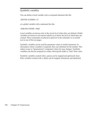
![787
Array variables
Array variables are like symbolic variables except that their values, which may
be real or complex, are accessed by indices which select an element of the array.
One Dimensional Array Syntax
.ARRAY arrayname V1[,V2 [,V3...[,Vn]]...] where the V values can be real or
complex. Note that there must be at least one element (V1) in the array.
You can define a one-dimensional array of real values like this:
.ARRAY RV 50,100,150
To access the values you use an index variable that typically is created like this:
.DEFINE IND 1
The index name may be any non-reserved name. You can access the array con-
tents like this:
RV(IND)
For example, you could set the RESISTANCE attribute of a resistor to RV(IND)
and then the resistor value takes on the RV array element that IND is set to. If
IND is set with the .define statement to 1, then the resistor value would be 100.
If IND is stepped through the values 0, 1, and 2, then the resistor value would be
50, 100, and 150 respectively.
Note that a one-dimensional array of size N+1 has values located at 0, 1, 2, ...N.
Two Dimensional Array Syntax
.ARRAY arrayname (m,n)
{v11,v12,...v1n},
{v21,v22,...v2n},
{v31,v32,...v3n},
...
{vm1,vm2,...vmn}](https://image.slidesharecdn.com/rm102-130625052342-phpapp02/85/Rm10-2-787-320.jpg)
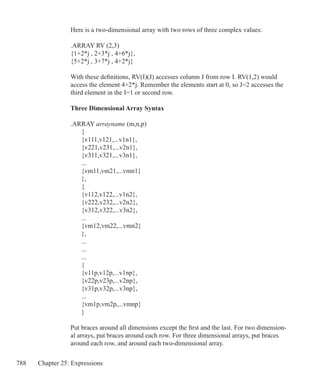
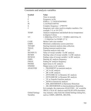

![792 Chapter 25: Expressions
Wildcard device and node names
A wildcard syntax is available for use in the Y Expression field of the Analysis
Limits dialog boxes. This syntax allows the user to compactly specify the plotting
of many similar expressions. The brackets [] and the letter @ are used as wild
cards. [] means to expand the contents between the brackets. @ refers to devices
while @@ refers to nodes:
Node examples:
D([@@]) means plot all digital node states: D(all_digital_nodes) and all analog
node voltages: V(all_analog_nodes).
V([@@]) means plot all analog node voltages: V(all_analog_nodes) and all digi-
tal node states: D(all_digital_nodes).
V([A@@]) means plot all node voltages that begin with A.
Device examples:
V([@]) means plot all device voltages: V(all_device_names).
V([R@]) means plot all device voltages: V(R1), V(R2),...V(Rall).
V([C1,C2,C3]) means plot the voltages: V(C1), V(C2), and V(C3).
V(L[1:3]) means plot the device voltages V(L1), V(L2), and V(L3).
V[C,B]([@]) means plot the voltages: VC(Q1), VC(Q2), ...VB(Q1), VB(Q2)...
I([L@]) means plot all device currents of the form: I(L1), I(LAB),...I(Lall).
I([@]) means plot all device currents.
[V,C,I,Q,X] ([C@,L@]) means plot all voltages (V), capacitances (C), currents
(I), charges (Q), or fluxes (X) whose device names begin with C or L. If a circuit
has two capacitors named C1 and C22 and one inductor named L3, it would plot
V(C1), V(C22), C(C1), C(C22), I(C1), I(C22), Q(C1), Q(C22), V(L3), I(L3), and
X(L3). Nonexistent terms, such as X(C1), X(C22) (capacitors usually have no
flux), C(L3) (inductors usually have no capacitance), and Q(L3) (inductors usual-
ly have no charge) are ignored. Note, that resistors, capacitors, and inductors will
have resistance, charge, and flux if they employ a model with those parasitics.](https://image.slidesharecdn.com/rm102-130625052342-phpapp02/85/Rm10-2-792-320.jpg)
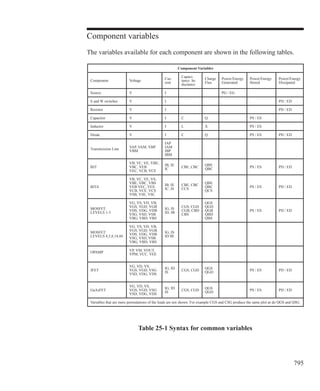
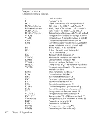
![804 Chapter 25: Expressions
Limiting and conditional operators
MIN(z1,z2) Minimum of real and imaginary parts of z1 and z2
MAX(z1,z2) Maximum of real and imaginary parts of z1 and z2
LIMIT(z,z1,z2) Returns z, with its real part limited to the range of
RE(z1) to RE(z2) and the imaginary part limited to the
range IM(z1) to IM(z2)
IF(b,z1,z2) If b is true, the function returns z1, else it returns z2.
Signal Processing / FFT Functions
HARM(u[,bw]) Harmonics of waveform u. bw = optional bandwidth
HARMN(u[,f0]) HARM divided by the value at the first harmonic or f0.
THD(S[,F]) Total harmonic distortion of spectrum S as a percent of
the value at the reference frequency F. If F is missing, it
is set to the first harmonic (1/tmax in transient analysis).
IHD(S[,F]) Individual harmonic distortion of S as a percent of the
value at F. It is similar to THD but not cumulative.
FFT(u) Standard forward Fourier transform of waveform u
FFTS(u[,bw]) Forward Fourier transform of waveform u, scaled so that
RE(FFTS(u)) produces the Fourier series cosine
coefficients and IM(FFTS(u)) produces the Fourier
series sine coefficients. BW = optional bandwidth.
FS(u[,n1[,n2]]) Partial Fourier series representation of waveform u,
compiled from the terms n1 through n2. N1 defaults to 0
and n2 defaults to the FFT Number of Points / 2.
RES(u[,n1[,n2]]) The residue function shows the waveform u minus the
Fourier terms n1 through n2. N1 defaults to 0. N2
defaults to 1, so that RES(u) is RES(u,0,1) and thus
essentially shows the distortion components due to the
2'nd and higher harmonics.
IFT(S) Standard inverse Fourier transform of spectrum S
IFTS(S) Scaled inverse Fourier transform of spectrum S. Scaling
is such that IFTS(FFTS(u)) = u.
CONJ(S) Conjugate of spectrum S
CS(u,v) Cross spectrum = CONJ(FFT(v))*FFT(u)*dt*dt
AS(u) Auto spectrum of waveform u = CS(u,u)
CC(u,v) Cross correlation of u and v = IFT(CS(u,v))/dt
AC(u) Auto correlation of waveform u is = IFT(AS(u))/dt
COH(u,v) Coherence of u and v =CC(u,v)/sqr(AC(u(0))*AC(v(0)))
REAL(S) Real part of spectrum S produced by FFT
IMAG(S) Imaginary part of spectrum S produced by FFT
MAG(S) Magnitude of spectrum S produced by FFT
PHASE(S) Phase of spectrum S produced by FFT](https://image.slidesharecdn.com/rm102-130625052342-phpapp02/85/Rm10-2-804-320.jpg)
![805
Numeric integration and differentiation:
With respect to any variable
DER(u,x) Calculates the analytical derivative of u W.R.T x. U
must be an explicit expression like SIN(2*PI*1E6*T).
SUM(y,x[,start]) Running integral of y with respect to x, with optional
start parameter. Integral begins at x=start. Start is only
used when x is the analysis variable and defaults to its
minimum (0, fmin, or dcmin).
With respect to the analysis variable (T, F, or DCINPUT1)
SD(y[,start]) Running integral of y with respect to T in transient, F in
AC, or DCINPUT1 in DC, with an optional start
parameter. Integral begins at start. Start defaults to
0, fmin, dcmin, according to the analysis type
DD(y) Numerical derivative of y with respect to T in transient,
F in AC, or DCINPUT1 in DC
RMS(y[,start]) Running root-mean-square of y with respect to F in AC,
T in transient, or DCINPUT1 in DC, with an optional
start parameter. Integral begins at start which defaults to
0, fmin, or dcmin, according to the analysis type.
AVG(y[,start]) Running average of y with respect to T in transient, F in
AC, or DCINPUT1 in DC. The optional start parameter
defaults to 0, fmin, dcmin.
With respect to T (Time) only
SDT(y[,start]) Running integral of y with respect to T (Time). Integral
begins at start. Start defaults to 0.
DDT(y) Numerical derivative of y with respect to T (Time)
DEL(y) Change in y from the prior data point to the current
point. A numerical derivative is formed by the ratio of
two operators. For example, DEL(y)/DEL(t)
approximates the numerical time derivative of y.
LAST(y,n) The n'th prior value of y. N=1 returns the value of y at
the last timestep. N=2 returns the value of y at the
timestep before last and so on.
Special functions
ABS(z) Absolute value function = (|z|2
)0.5
BUFFER(W) Imports the W waveform from the Waveform Buffer.](https://image.slidesharecdn.com/rm102-130625052342-phpapp02/85/Rm10-2-805-320.jpg)
![806 Chapter 25: Expressions
CURVEY(F,W) Imports the Y component of curve W from the User
source F. F must be saved in standard format using the
Save Curves section of the Plot Properties dialog box.
See User source in Chapter 22 for the file format.
CURVEX(F,W) Imports the X component of curve W from file F.
DELAY(x,d) Returns expression x delayed by d seconds.
DIFA(u,v[,d]) DIFA reports differences between two analog curves. It
compares the u expression with the v expression at every
analysis point, and returns 1 if the absolute value of the
result is more than d. Otherwise, it returns 0. U and v
may be imported curves. See the IMPORT function. D
is optional and defaults to 0.
DIFD(u,v[,d]) DIFD reports differences between two digital curves. It
compares the u level with the v level at every analysis
point, and returns 1 if they differ for a time exceeding d.
Otherwise, it returns 0. U and v may be imported curves.
D is optional and defaults to 0.
FACT(u) Factorial of the integer value of u.
U! Factorial of the integer value of u. When using the !
notation, u must be a symbolic variable or a constant.
G(X1) Complex conductance of two-terminal device X1. X1
must be a resistor, capacitor, inductor, or diode.
IMPORT(f,y) Imports curve y from the file f. The file must be a SPICE
or MC10 output text file with a table of values that
includes the value F(frequency), T(Time), V(source
voltage), or I(current source), and the value of the
expression y. Y must be typed exactly as shown in the
file and must contain an even number of parentheses.
INT(x) Truncated integer function. INT(2.7) = 2
NINT(x) Round-up integer function. INT(2.7) = 3
IMPULSE(y) Impulse function of amplitude y and area of 1.0.
JN(n,z[,m]) N'th order Bessel function of the first kind of the
complex expression z, compiled from the series using m
terms. M defaults to 10.
J0(z) Zero'th order Bessel function of the first kind of the
complex expression z. Same as JN(0,z,10)
J1(z) First order Bessel function of the first kind of the
complex expression z. Same as JN(1,z,10)
LAST(z,n) Curve z delayed by n time points. LAST(z,1)i
= zi-1
MAXR(x) Returns the largest value of x encountered at any time
during a transient or DC sweep analysis run.](https://image.slidesharecdn.com/rm102-130625052342-phpapp02/85/Rm10-2-806-320.jpg)
![807
MINR(x) Returns the smallest value of x encountered at any time
during a transient or DC sweep analysis run.
NORM(z,x0) Curve z normalized at the value of z when the X
expression is equal to x0. DB operators normalized to 0.
NORMMAX(z) Curve z normalized at the maximum value of z
NORMMIN(z) Curve z normalized at the minimum value of z
PN(n,x) N'th order Legendre polynomial function of x.
PROD(n,n1,n2,z) Calculates the product of the series of the complex
expression z = z(n), for n = n1 to n = n2. For example,
PROD(n,1,3,j+n) = (j+1)*(j+2)*(j+3) = 0 +10j
SERIES(n,n1,n2,z) Calculates the summation of the series of the complex
expression z = z(n), for n = n1 to n = n2. For example,
SERIES(n,1,3,n+j) = (j+1) + (j+2) + (j+3) = 6 + 3j
SGN(y) +1 (if y0), 0 (if y=0), -1 (if y0)
SQRT(z) Complex square root = z0.5
STP(x) Step function of amplitude 1.0 starting at T = x.
TABLE(x,x1
,y1
..xn
,yn
)
This function performs a table lookup. It returns a value
for y associated with the value of x, interpolated from
the table. X values less than x1
generate an answer of y1
.
X values greater than xn
generate an answer of yn
.
W(z) Lambert W function for complex z.
YN(n,z[,m]) N'th order Bessel function of the second kind of the
complex expression z, compiled from the series
using m terms. M defaults to 10.
Y0(z) Zero'th order Bessel function of the second kind of the
complex expression z. Same as YN(0,z,10)
Y1(z) First order Bessel function of the second kind of the
complex expression z. Same as YN(1,z,10)
Z(X1) Complex impedance of two-terminal device X1. X1
must be a resistor, capacitor, inductor, or diode.](https://image.slidesharecdn.com/rm102-130625052342-phpapp02/85/Rm10-2-807-320.jpg)
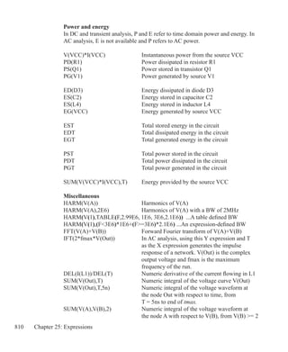
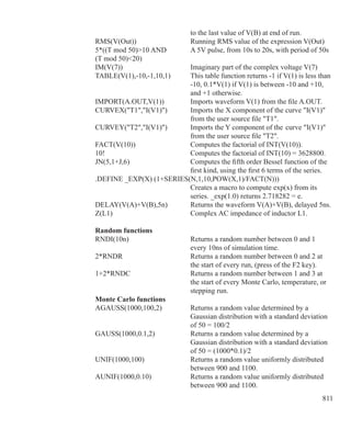

![815
.AC
General Form (SPICE files only)
.AC [[DEC] | [OCT] | [LIN]] data points fmin fmax
Examples
.AC DEC 30 20 20K
.AC LIN 10 100 200
The .AC command arguments are mapped into the appropriate Micro-Cap Analy-
sis Limits dialog box fields upon selecting AC from the Analysis menu. DEC
(decade), OCT (octal), and LIN (linear) specify the type of fixed frequency step
to be used during the AC analysis. DEC and OCT select the Log Frequency Step
option and LIN selects the Linear Frequency Step option on the AC Analysis
Limits dialog box.
data points specifies the number of data points per decade for the decade op-
tion or the total number of data points for the linear option. It is mapped into
the Number of Points field. fmin specifies the first frequency of the run and
fmax specifies the last. These are mapped into the Frequency Range field.
A waveform source need not be present in the circuit, but if there is no source, all
output will be zero. For waveform sources, the small signal model is simply an
AC voltage or current source. The AC value of the source is determined from the
parameter line for SPICE components and from the attribute value for schematic
components.
SPICE V or I sources:
The AC magnitude value is specified as a part of the device parameter. For
example, a source with the value attribute DC 5.5 AC 2.0 has an AC
magnitude of 2.0 volts.
Pulse and sine sources:
These sources have their AC magnitude fixed at 1.0 volt.
User sources: User sources provide a signal comprised of the real and
imaginary parts specified in their files.
Function sources: These sources create an AC signal only if a FREQ
expression is specified.](https://image.slidesharecdn.com/rm102-130625052342-phpapp02/85/Rm10-2-815-320.jpg)
![816 Chapter 26: Command Statements
.ARRAY
One Dimensional Array Syntax
.ARRAY arrayname V1[,V2 [,V3...[,Vn]]] V values are real or complex.
Examples
.ARRAY RESISTANCE 3.3K,4.5K,5.0K
.ARRAY WIDTHS .07u,1u,1.2u,1.5u,2u
The .ARRAY command declares an array of values that can be used by device
attribute fields and model parameters. Array elements are accessed from zero as
NAME(0), NAME(1) and so on either with a fixed integer or an integer variable.
For example, consider these statements:
.ARRAY CAP 1p,10p,15p,24p,36p
.DEFINE INDEX 0
With these declarations, you can use CAP(INDEX) as the CAPACITANCE at-
tribute of one or more capacitors and then step the INDEX variable to assign the
values 1p, 10p, 15p, 24p, 36p successively to the capacitors.
Here is another example:
.MODEL N1 NPN ( BF=BETA1(INDEX) CJE=1.8P CJC=0.8P TF=.5N )
.MODEL N2 NPN ( BF=BETA2(INDEX) CJC=1P CJE=2P TF=1N TR=1N )
.DEFINE INDEX 0
.ARRAY BETA1 100,200,300
.ARRAY BETA2 60,70,90
With these declarations, you can step INDEX, simultaneously accessing both
beta arrays, assigning unique pairs of values for use in the two model statements.
Two Dimensional Array Syntax
.ARRAY arrayname (m,n)
{v11,v12,...v1n},
{v21,v22,...v2n},
{v31,v32,...v3n},
...
{vm1,vm2,...vmn}](https://image.slidesharecdn.com/rm102-130625052342-phpapp02/85/Rm10-2-816-320.jpg)
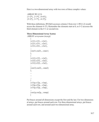
![818 Chapter 26: Command Statements
.DC
General Form (SPICE files only)
Linear sweep type
.DC [LIN] v1 start1 end1 increment1
+ [v2 start2 end2 increment2]
Log sweep type
.DC OCT | DEC
+ v1 start1 end1 points1 per octave or decade
+ [v2 start2 end2 points2 per octave or decade]
List sweep type
.DC v1 LIST value* [v2 LIST value*]
v1 and v2 must be one of the following:
1. The name of an independent source in the circuit. e.g. VCC
2. A model parameter name in the form:
model type model name(parameter name) e.g. NPN QF(BF)
3. Operating temperature in the form: TEMP
4. A symbolic parameter in the form:
PARAM symbolic parameter name e.g. PARAM temp1
Sweep specifications can be different for v1 and v2. That is, you can use
linear sweeping for one variable and log for the other.
Examples
.DC VIN1 -.001 .001 1U
.DC VCC 0 5 0.1 IB 0 0.005 0.0005
.DC DEC RES RMOD(R) 1m 100 5
.DC PARAM FILTER_Q 10 20 1
.DC VCC LIST 4.0 4.5 5.0 5.5 6.5 VEE LIST 24 25 26](https://image.slidesharecdn.com/rm102-130625052342-phpapp02/85/Rm10-2-818-320.jpg)
![819
.DEFINE
General Form (SPICE or schematics)
.DEFINE [{LOT[td]=n[%]}] text1 text2
where td is [ [/lot#][/GAUSS|UNIFORM|WCASE]]
Examples
.Define V1 (2*t*sin(2*pi*T))
.DEFINE RVAL 128.5K
.DEFINE {LOT=10%} LVAL 1200MH
.DEFINE {LOT/1/GAUSS=10%} CVAL 1200NF
This form of the statement is used to create and define the value of a symbolic
variable. It substitutes text2 for text1 everywhere except for text from the
PART attribute Value field and model parameter name text. While you can't use
this statement to change the name of a part or a model parameter name, you can
use it to change the name of the model itself.
General Form (Schematics only)
.DEFINE name(p1[,p2][...,pn]) f(p1[,p2][...,pn])
where f() is some expression involving the parameters p1[,p2][.. .,pn]
This form of the statement works exactly like C language macros, substituting in
at run time the values of p1[,p2][...,pn]. It is also similar to the SPICE
.FUNC statement. When placing define statements into a schematic page, only a
single define statement can be placed in at a time.
Examples: String replacement
A good example of string replacement occurs in digital STIM devices. These de-
vices require a COMMAND attribute string to describe their behavior. A typical
command might be:
.define SQUAREWAVE
+ 0NS 0
+ LABEL=START
+ +10NS 1
+ +10NS 0
+ +10NS GOTO START 10 TIMES](https://image.slidesharecdn.com/rm102-130625052342-phpapp02/85/Rm10-2-819-320.jpg)
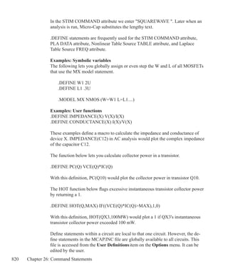
![822 Chapter 26: Command Statements
.END
General Form (SPICE files only)
.END
Examples
.END
This statement specifies the end of a SPICE netlist. These blocks are placed in the
text area of a circuit. All circuit descriptions and commands must come before
the .END statement.
.ENDIF
General Form (SPICE files and schematic text areas only)
.ENDIF
Example
.ENDIF
This statement terminates a .IF statement block. Together the .IF and .ENDIF
encapsulate a control block. For example:
.IF BEST_CASE
.DEFINE C1 1.2pF
.ENDIF
.ENDS
General Form (SPICE files and schematic text areas only)
.ENDS [subcircuit name]
Examples
.ENDS
.ENDS FILTER
This statement terminates a subcircuit description. The optional subcircuit name
label is used only for clarification.](https://image.slidesharecdn.com/rm102-130625052342-phpapp02/85/Rm10-2-822-320.jpg)
![823
.ENDSPICE
General Form (Text area only)
.ENDSPICE
Examples
.ENDSPICE
This statement specifies the end of a .SPICE control block. These blocks are
placed in the text area of a circuit. For example
.SPICE
.MODEL DD D ()
D1 OUT A DD
C10 A 0 100N
.ENDSPICE
This set of commands creates a small network with a diode and a capacitor and
connects it to the OUT node in the main circuit. Node A is available for plotting.
.FUNC
General Form (SPICE or schematics)
.FUNC name(p1[,p2][...,pn]) f(p1[,p2][...,pn])
This command is similar to the macro form of the .DEFINE command and is
included as a separate command because it is sometimes used in commercial
models. The function name must not be the same as any of the predefined func-
tions such as sin, cos, exp, etc.
Examples
.FUNC MAX3(A,B,C) MAX(MAX(A,B),C)
.FUNC QUAD(A,B,C,X) A*X^2+B*X+C
.FUNC DIVIDER(A,B,C) V(B,C)/V(A,C)](https://image.slidesharecdn.com/rm102-130625052342-phpapp02/85/Rm10-2-823-320.jpg)
![824 Chapter 26: Command Statements
.HELP
General Form (Schematics only)
.HELP parameter name help text
This command places parameter help text in a macro schematic. The help text is
displayed in the Status bar of the Attribute dialog box when a macro is placed or
edited and the cursor is over the parameter name.
parameter name should be one of the macro parameters listed in the
.PARAMETERS statement.
Here are several examples:
.HELP VP Peak magnitude of the output signal
.HELP KF Frequency sensitivity in Hz/Volt
.IC
General Forms (SPICE or schematics)
Analog nodes
.IC V(analog node1[,analog node2]) = voltage value*
Inductors
.IC I(inductor) = current value*
Digital nodes
.IC D(digital node) = digital value*
Examples
.IC V(VOUT)=2.0
.IC I(L1)=6.0 V(3)=2
.IC D(1440)=0
.IC D(DIN)=X D(12)=1
The .IC statement assigns initial voltages, inductor currents, and digital logic
states during the AC and transient analysis operating point calculation, and dur-
ing the first data point in DC analysis. It assigns the analog or digital value to the
node or branch and holds the value during the entire operating point calculation.](https://image.slidesharecdn.com/rm102-130625052342-phpapp02/85/Rm10-2-824-320.jpg)
![826 Chapter 26: Command Statements
.INCLUDE
General Form (SPICE or schematics)
.INC[LUDE] Filename
Examples
.INCLUDE C:Micro-CapDATAEX1DEF.TXT
.INC C:Micro-CapDATAMYSMALL.LIB
This statement includes text from an external text file in a schematic or SPICE
file prior to an analysis. This is useful if you have an external library of model
statements in text file format. Use the Text tool in the Schematic Editor to add the
statement to a schematic. Filename may include a path. The quotation marks
are optional.
This command includes](https://image.slidesharecdn.com/rm102-130625052342-phpapp02/85/Rm10-2-826-320.jpg)
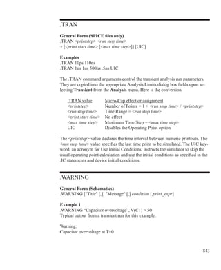
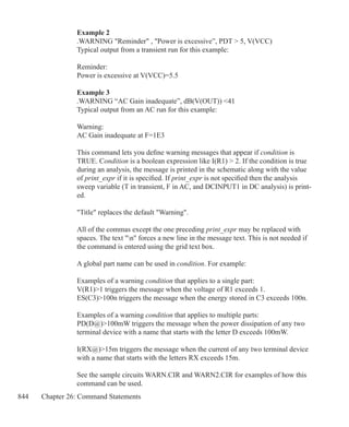


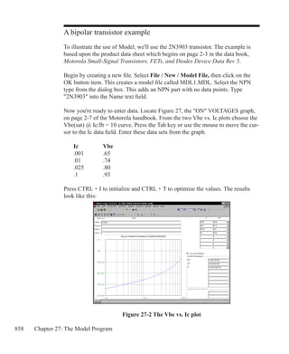
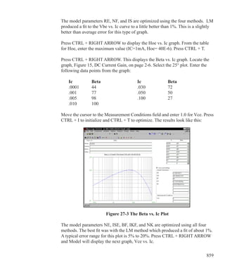
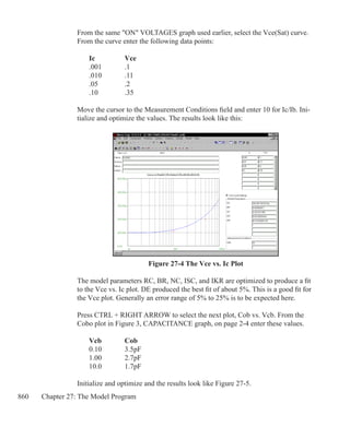
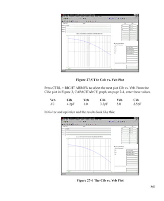
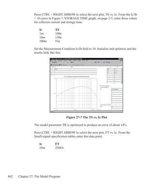
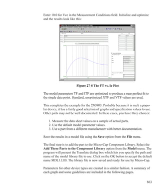
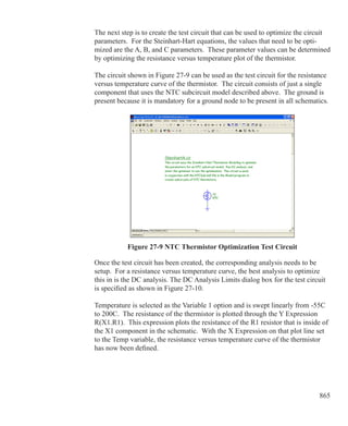
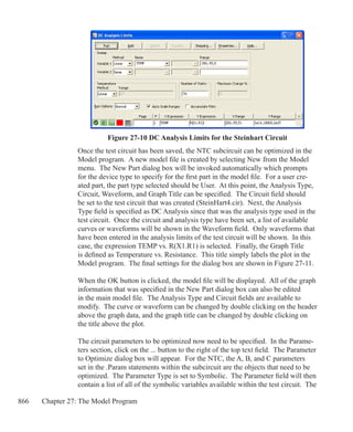
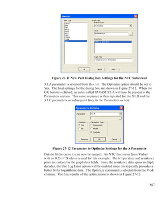
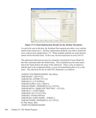
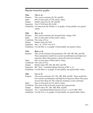
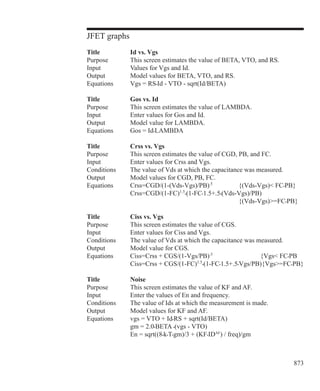
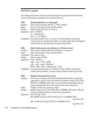
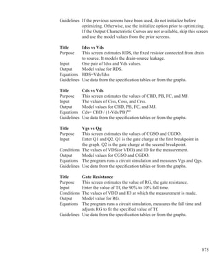
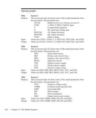
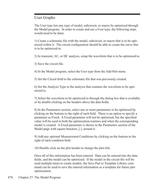
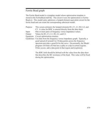
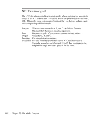

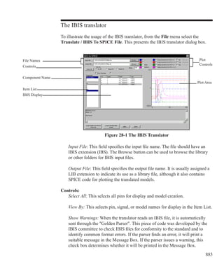
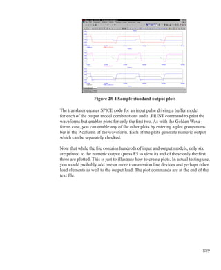


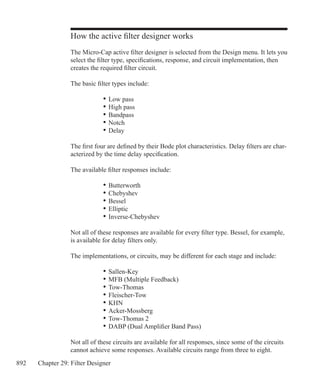
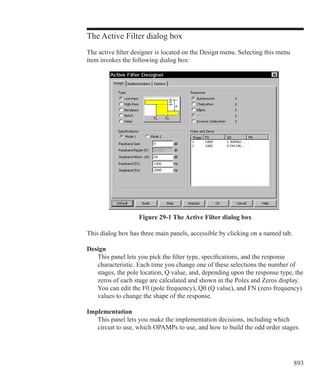
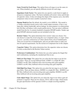
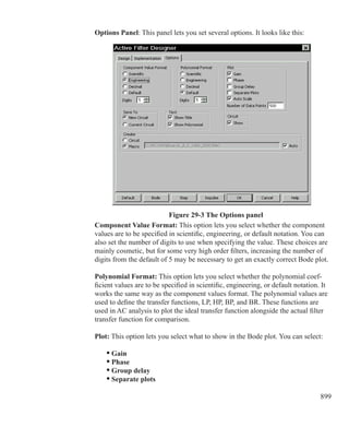
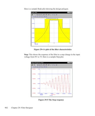
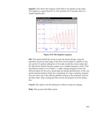

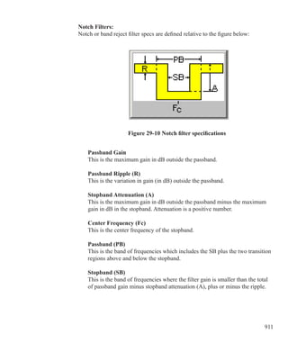


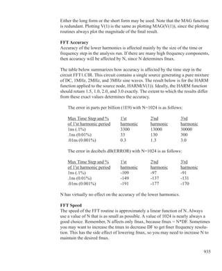
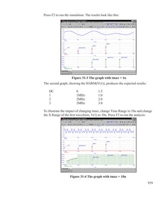
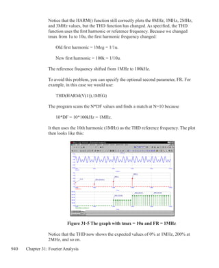
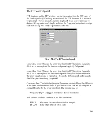
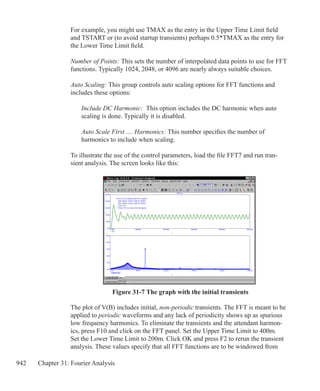
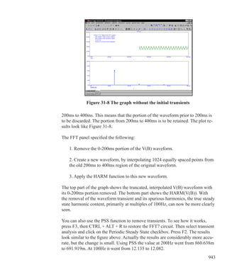


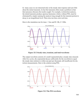
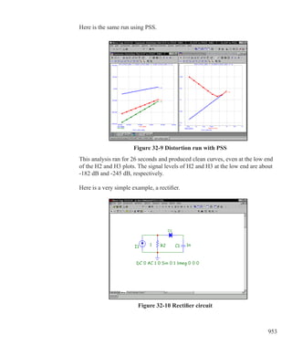
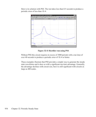
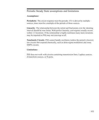


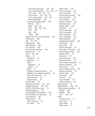
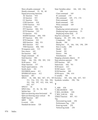

This document provides a 3-page summary of the contents and structure of the Micro-Cap 10 circuit analysis software reference manual. It includes the copyright information, a brief table of contents that lists the 27 chapters and their topics, and a few example sections and commands that are described in the manual.