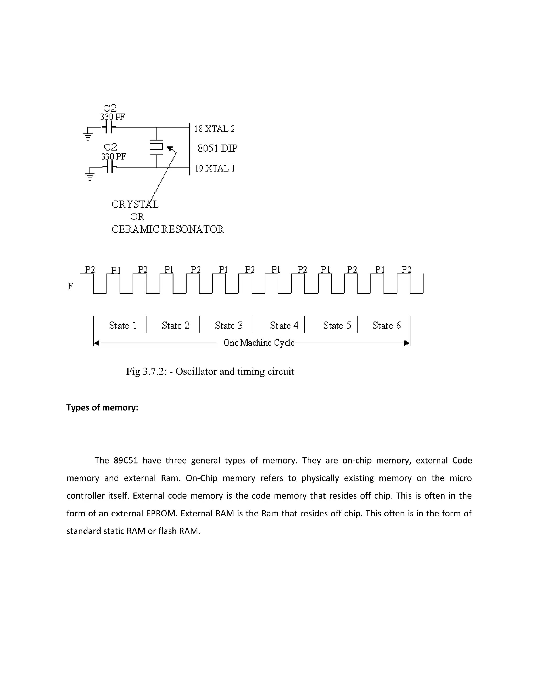
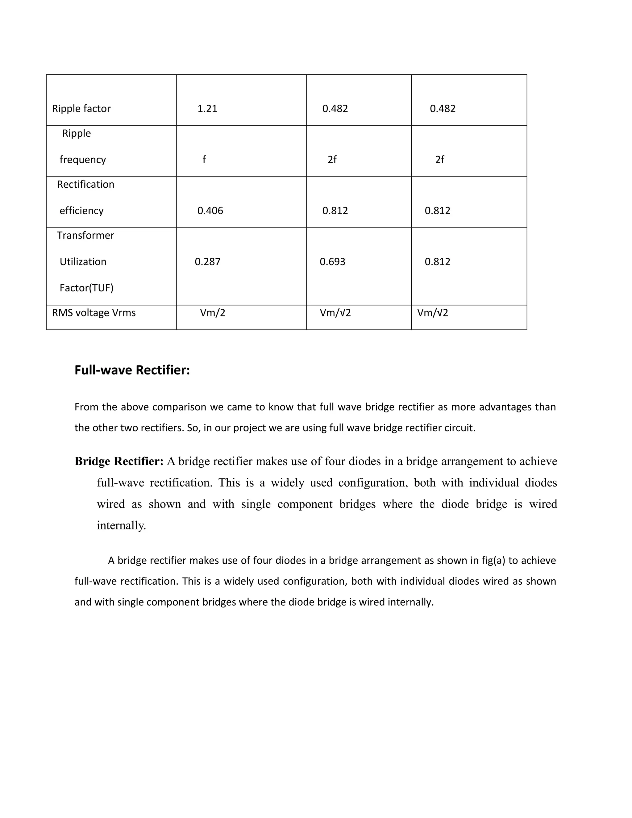
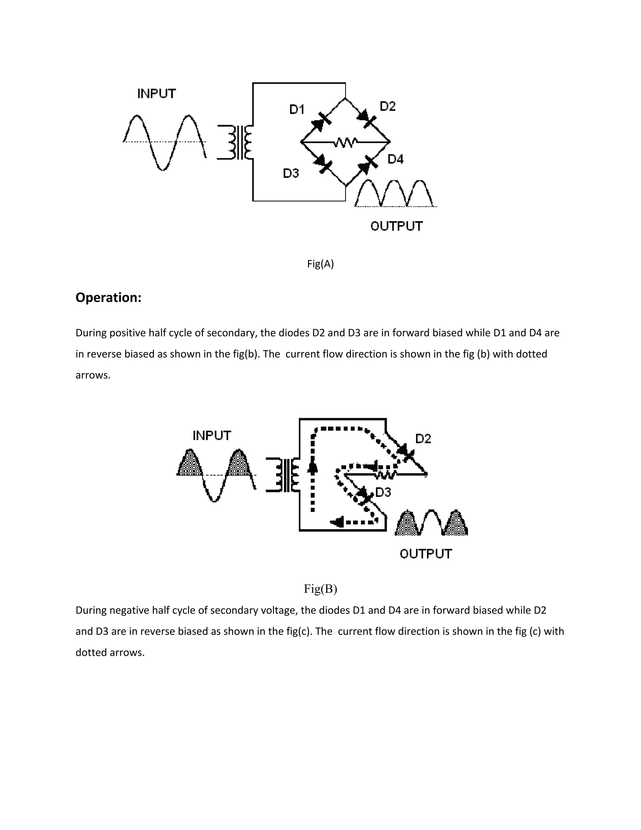
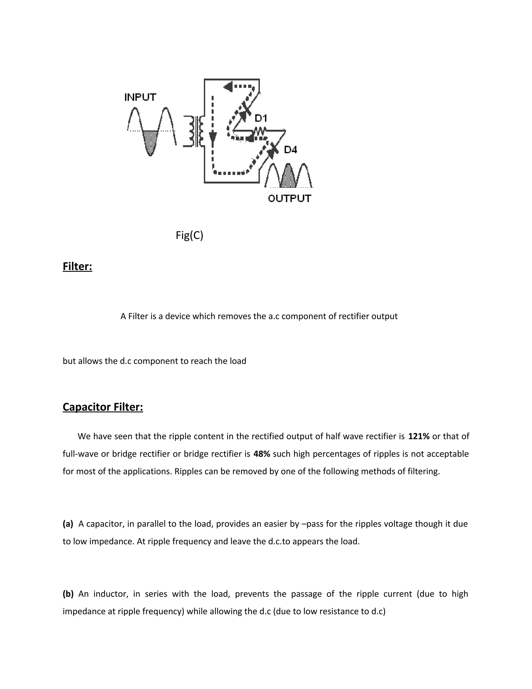
Downloaded 544 times


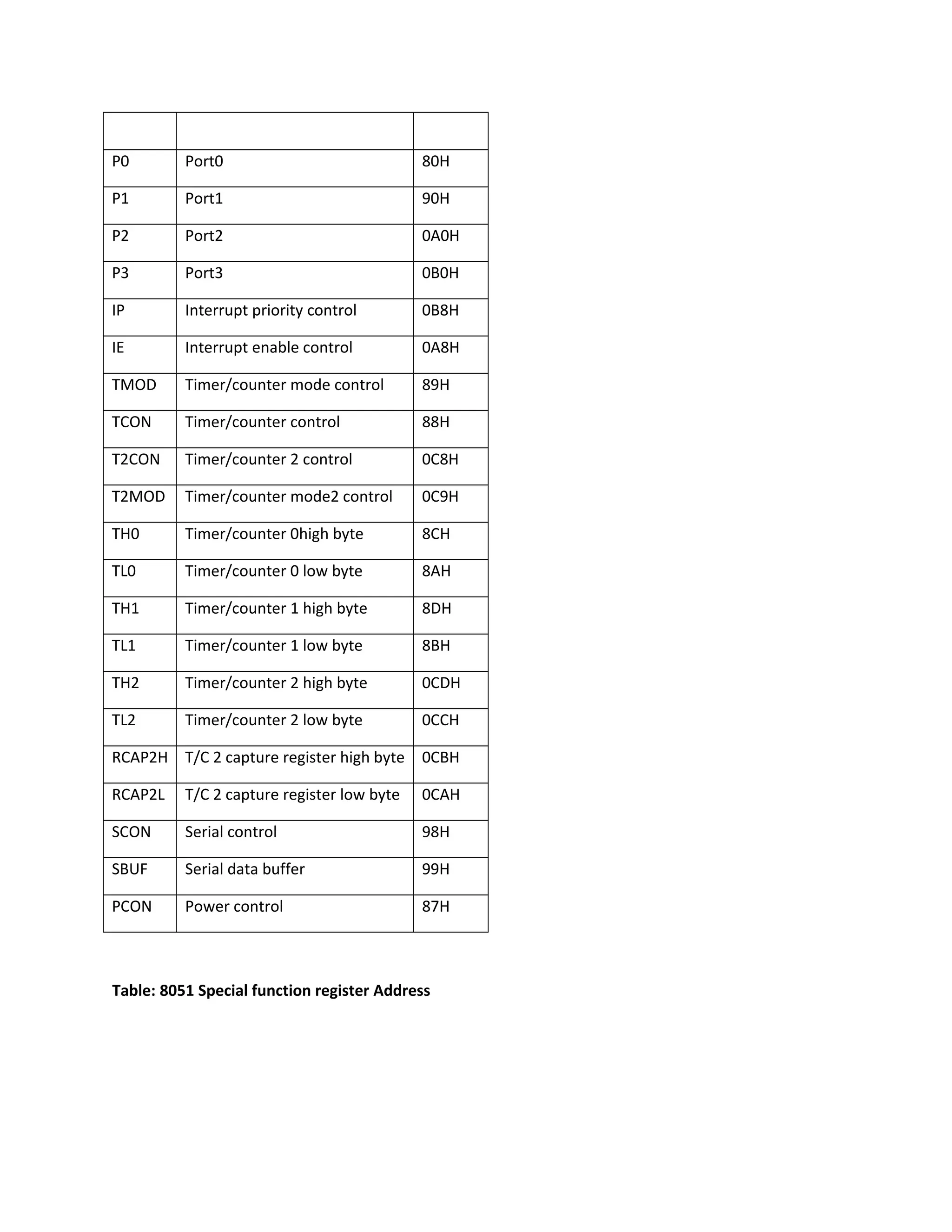


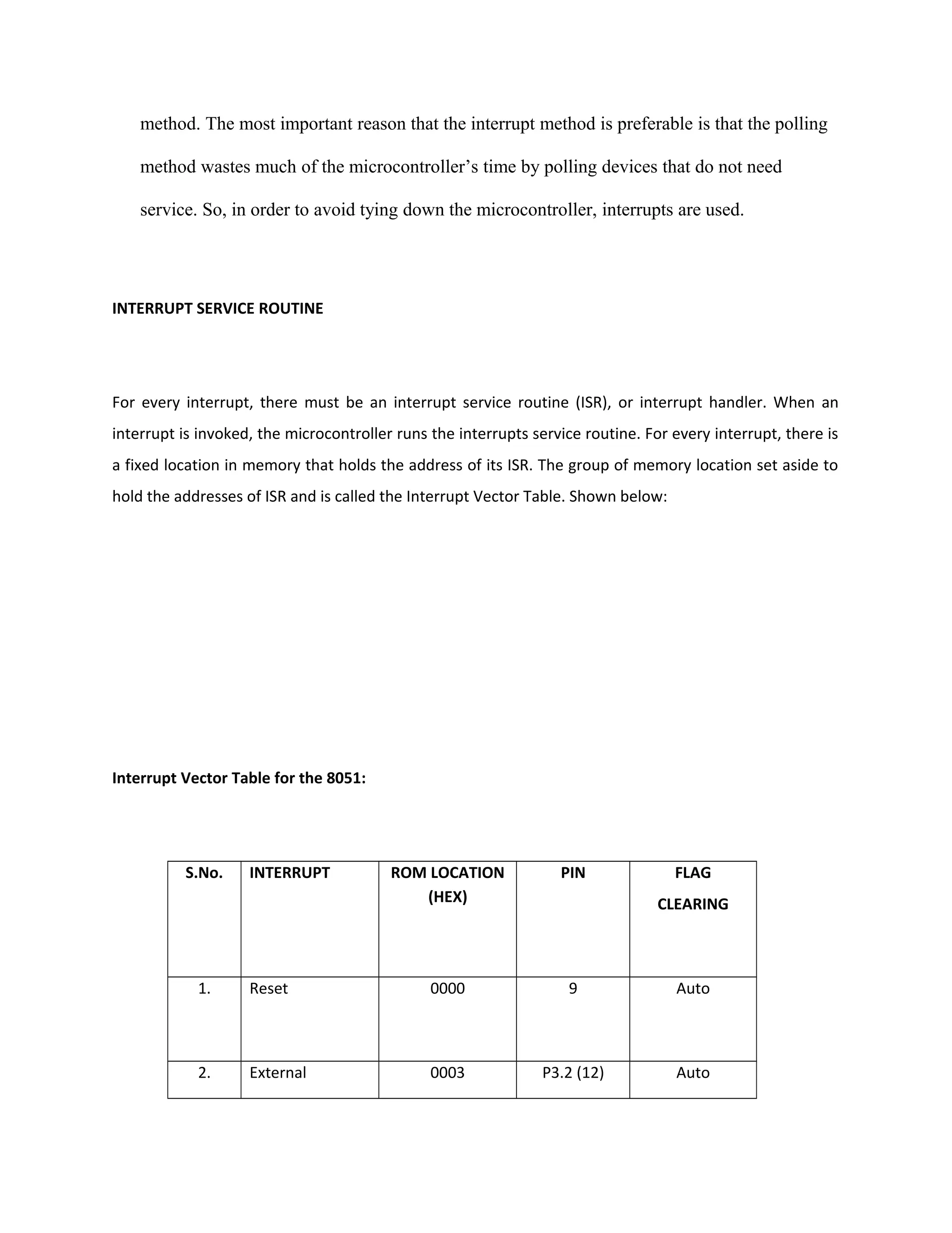
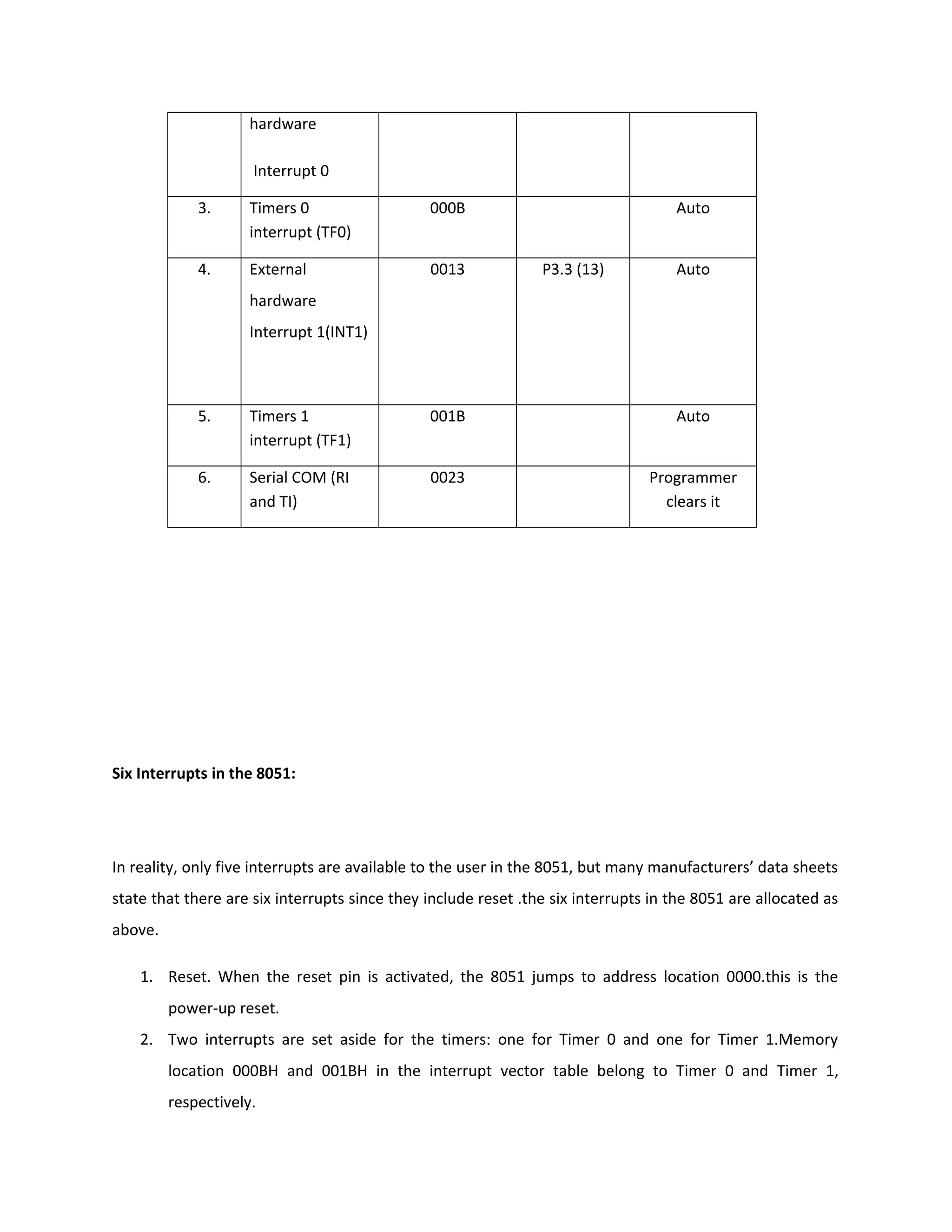


![A Passive InfraRed sensor (PIR sensor) is an electronic device that measures infrared (IR)
light radiating from objects in its field of view. PIR sensors are often used in the construction of
PIR-based motion detectors (see below). Apparent motion is detected when an infrared source
with one temperature, such as a human, passes in front of an infrared source with another
temperature, such as a wall.[1]
All objects emit what is known as black body radiation. It is usually infrared radiation that is
invisible to the human eye but can be detected by electronic devices designed for such a
purpose. The term passive in this instance means that the PIR device does not emit an infrared
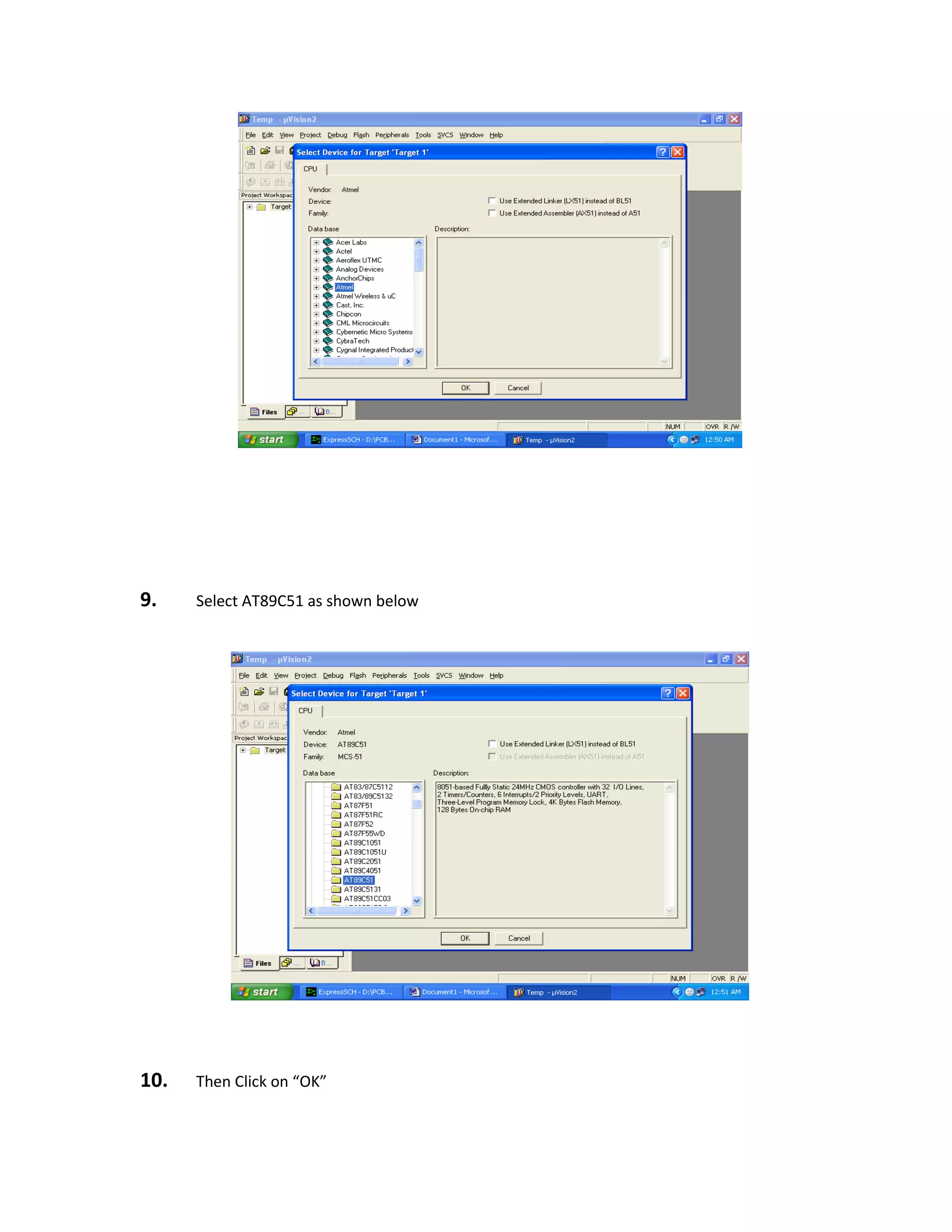
beam but merely passively accepts incoming infrared radiation. “Infra” meaning below our ability
to detect it visually, and “Red” because this color represents the lowest energy level that our
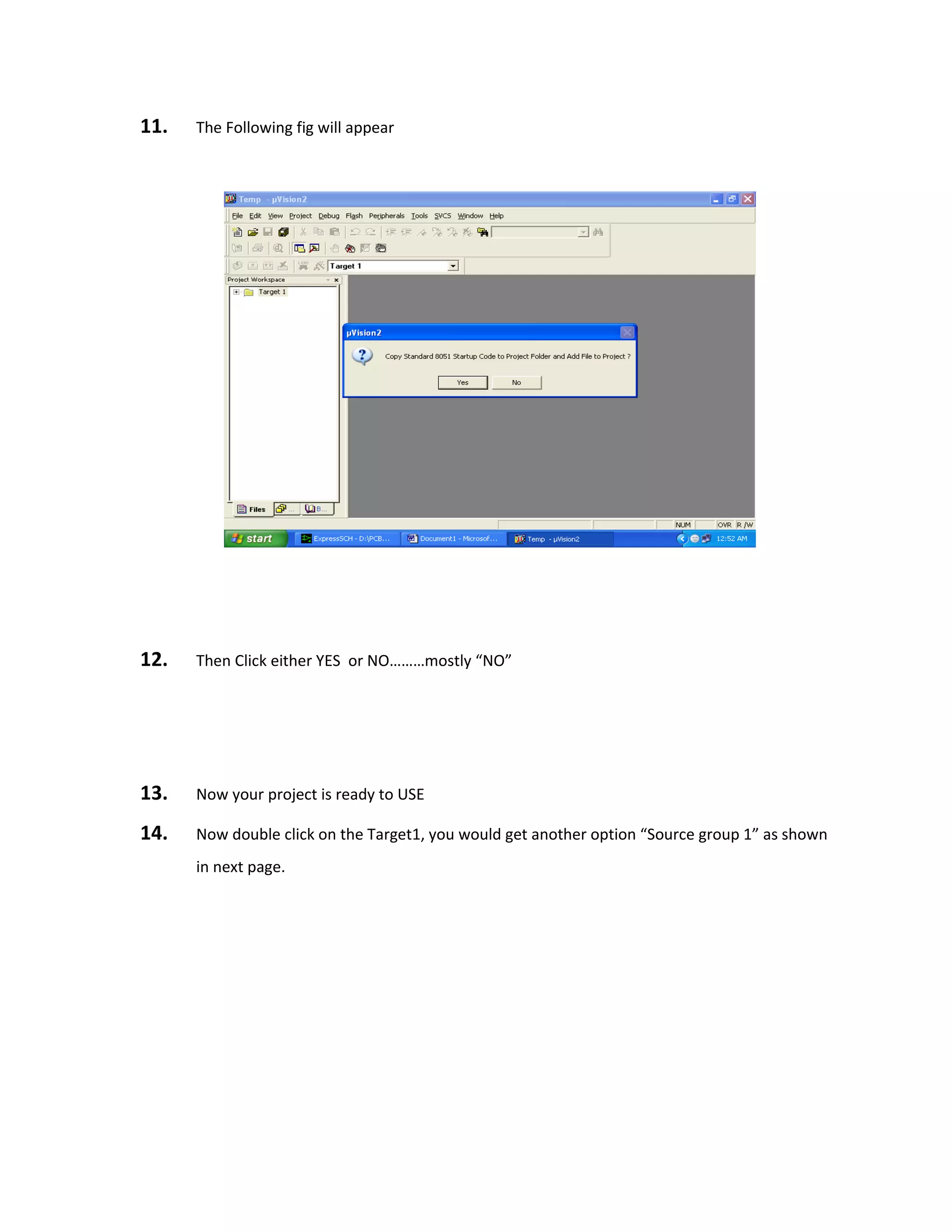
eyes can sense before it becomes invisible. Thus, infrared means below the energy level of the
color red, and applies to many sources of invisible energy.[2]
In a PIR-based motion detector (usually called a PID, for Passive Infrared Detector), the PIR
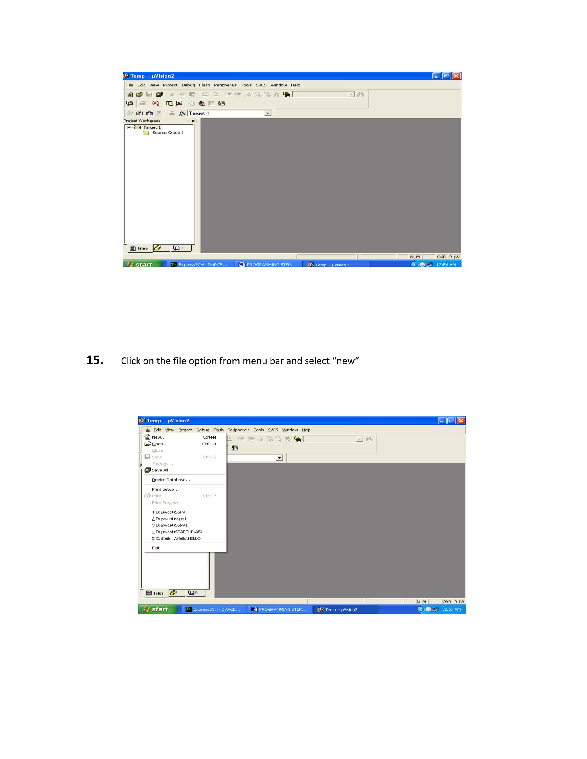
sensor is typically mounted on a printed circuit board containing the necessary electronics
required to interpret the signals from the pyroelectric sensor chip. The complete assembly is
contained within a housing mounted in a location where the sensor can view the area to be
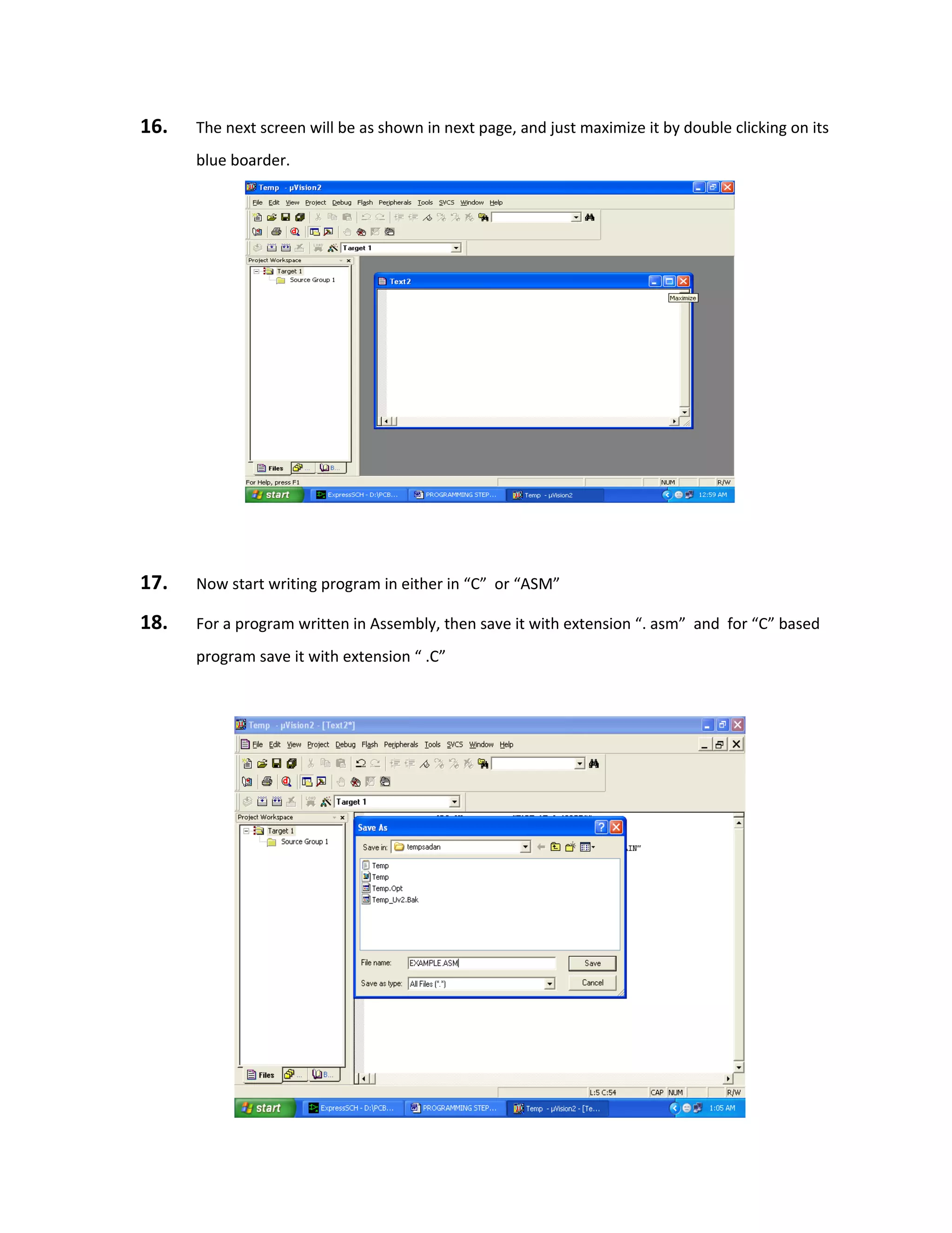
monitored. Infrared energy is able to reach the pyroelectric sensor through the window because
the plastic used is transparent to infrared radiation (but only translucent to visible light). This
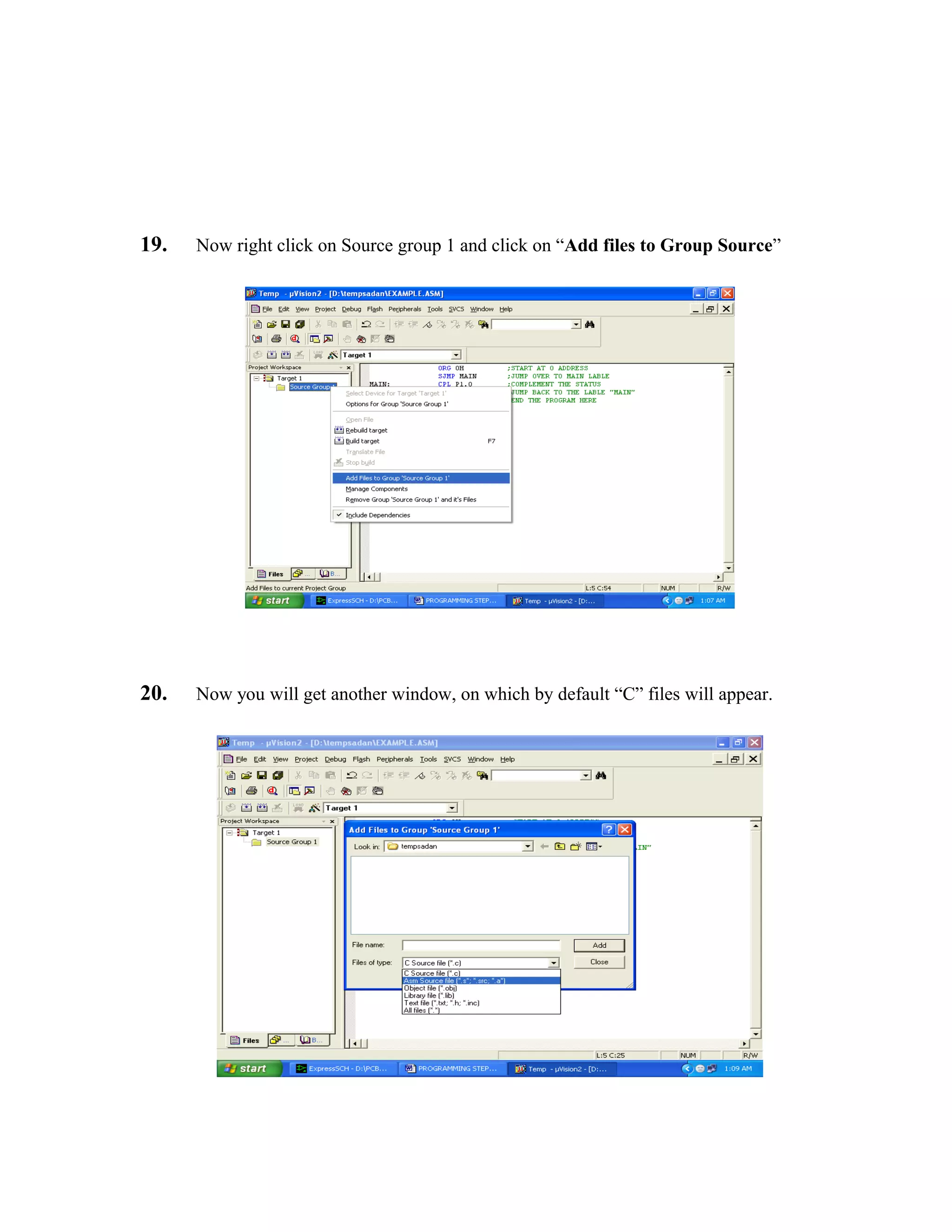
plastic sheet also prevents the intrusion of dust and/or insects from obscuring the sensor's field
of view, and in the case of insects, from generating false alarms.
A few mechanisms have been used to focus the distant infrared energy onto the sensor surface.
The window may have multiple Fresnel lenses molded into it.
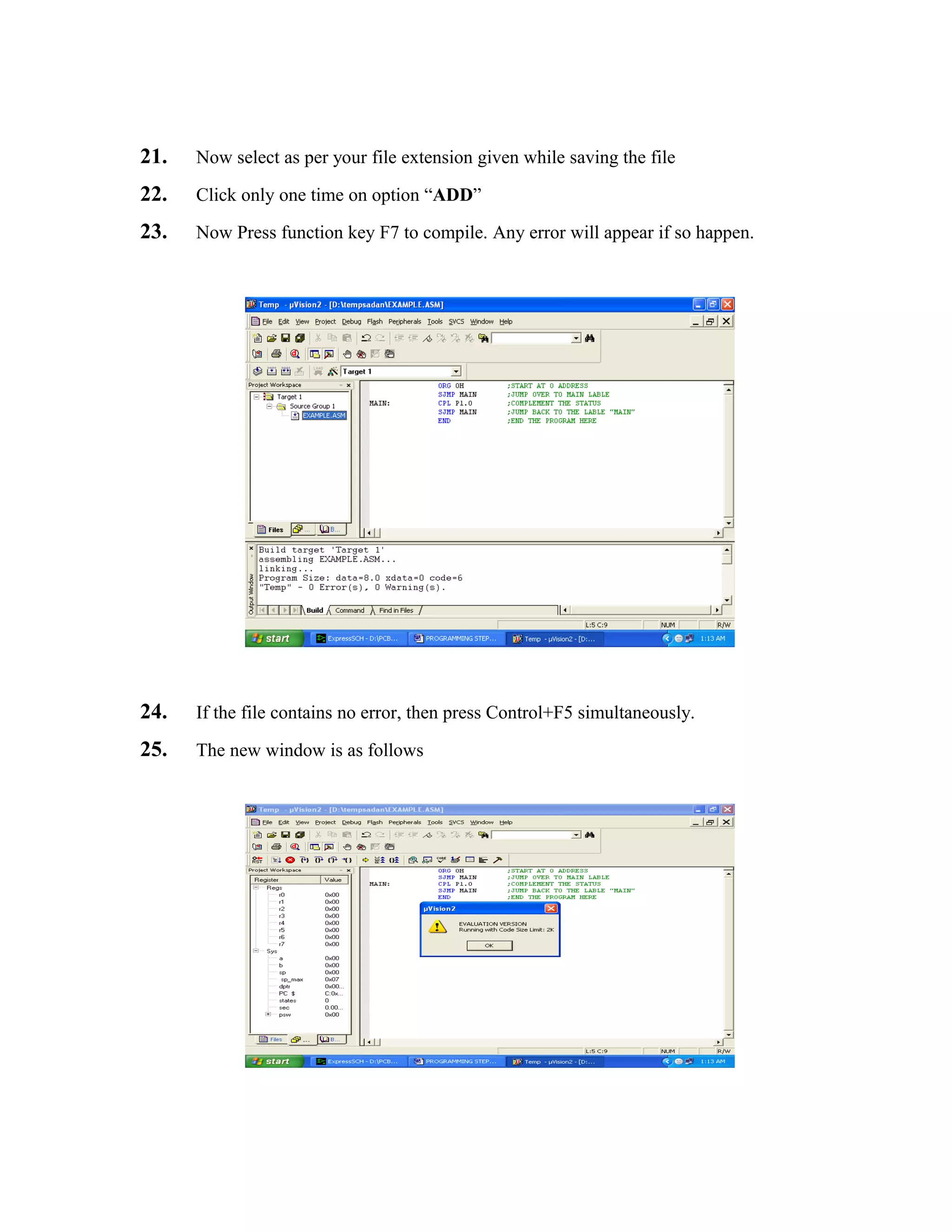
A person entering a monitored area is detected when the infrared energy emitted from the
intruder's body is focused by a Fresnel lens or a mirror segment and overlaps a section on the
chip that had previously been looking at some much cooler part of the protected area. That
portion of the chip is now much warmer than when the intruder wasn't there. As the intruder
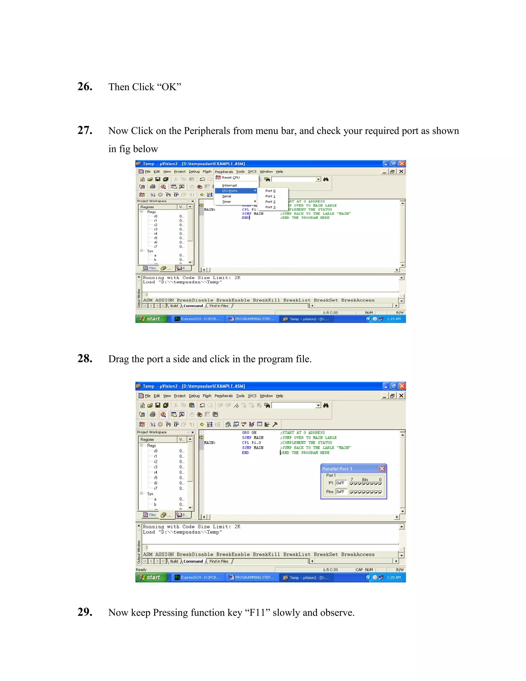
moves, so does the hot spot on the surface of the chip. This moving hot spot causes the
electronics connected to the chip to de-energize the relay, operating its contacts, thereby
activating the detection input on the alarm control panel. Conversely, if an intruder were to try to
defeat a PID, perhaps by holding some sort of thermal shield between himself and the PID, a
corresponding 'cold' spot moving across the face of the chip will also cause the relay to de-
energize — unless the thermal shield has the same temperature as the objects behind it.
Manufacturers recommend careful placement of their products to prevent false (non-intruder
caused) alarms. They suggest mounting the PIDs in such a way that the PID cannot 'see' out of
a window. Although the wavelength of infrared radiation to which the chips are sensitive does
not penetrate glass very well, a strong infrared source such as from a vehicle headlight or
sunlight reflecting from a vehicle window can overload the chip with enough infrared energy to
fool the electronics and cause a false alarm. A person moving on the other side of the glass
however would not be 'seen' by the PID.](https://image.slidesharecdn.com/12-130806042257-phpapp02/75/12-automatic-toll-gate-billing-system-using-rfid-77-2048.jpg)
![They also recommended that the PID not be placed in such a position that an HVAC vent would
blow hot or cold air onto the surface of the plastic which covers the housing's window. Although
air has very low emissivity (emits very small amounts of infrared energy), the air blowing on the
plastic window cover could change the plastic's temperature enough to, once again, fool the
electronics.
PIDs come in many configurations for a wide variety of applications. The most common, used in
home security systems, have numerous Fresnel lenses or mirror segments and an effective
range of about thirty feet. Some larger PIDs are made with single segment mirrors and can
sense changes in infrared energy over one hundred feet away from the PID. There are also
PIDs designed with reversible orientation mirrors which allow either broad coverage (110° wide)
or very narrow 'curtain' coverage.
PIDs can have more than one internal sensing element so that, with the appropriate electronics
and Fresnel lens, it can detect direction. Left to right, right to left, up or down and provide an
appropriate output signal.
[edit] PIR-based remote thermometer
Designs have been implemented in which a PIR circuit measures the temperature of a remote
object.[3]
In such a circuit, a non-differential PIR output is used. The output signal is evaluated
according to a calibration for the IR spectrum of a specific type of matter to be observed. By this
means, relatively accurate and precise temperature measurements may be obtained remotely.
Without calibration to the type of material being observed, a PIR thermometer device is able to
measure changes in IR emission which correspond directly to temperature changes, but the
actual temperature values cannot be calculated.
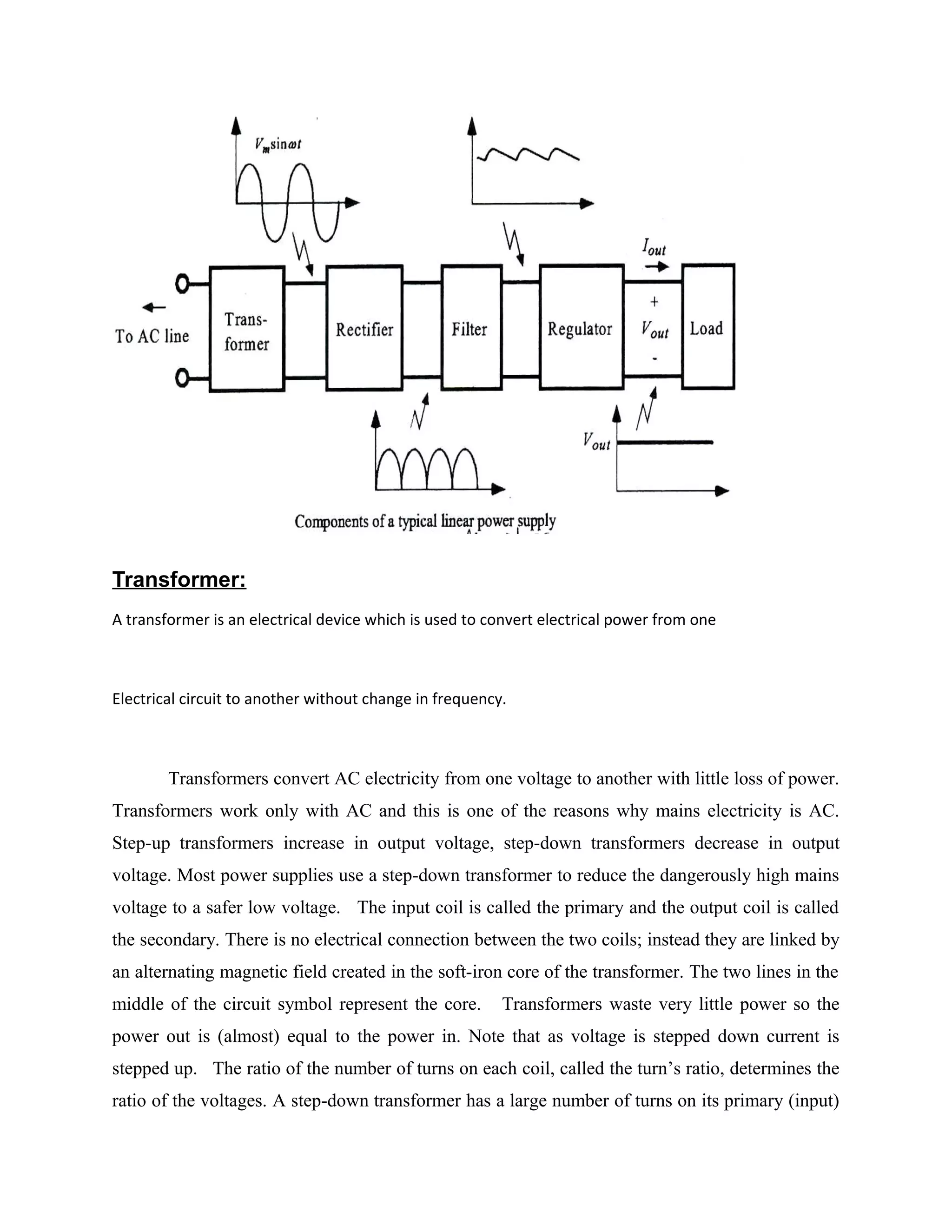
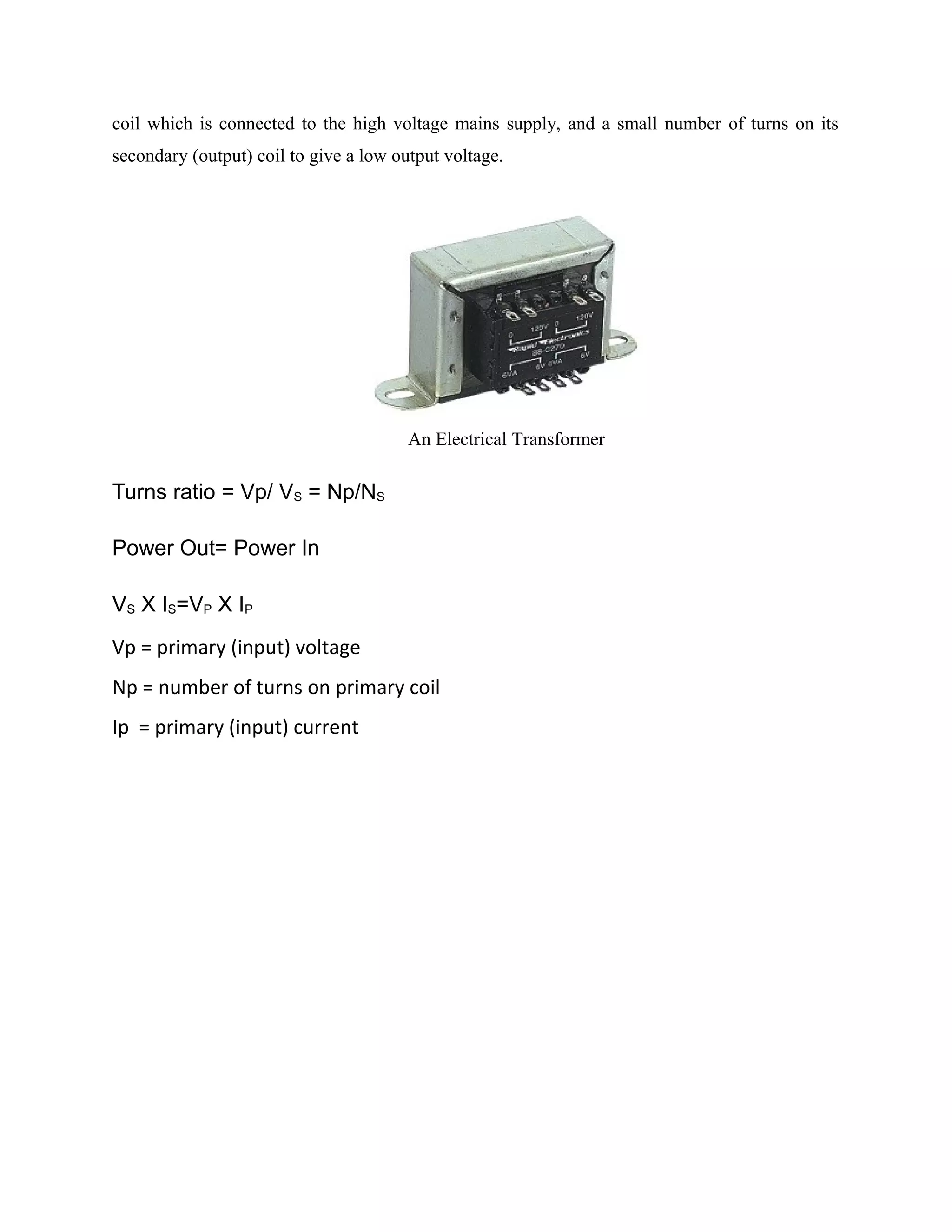
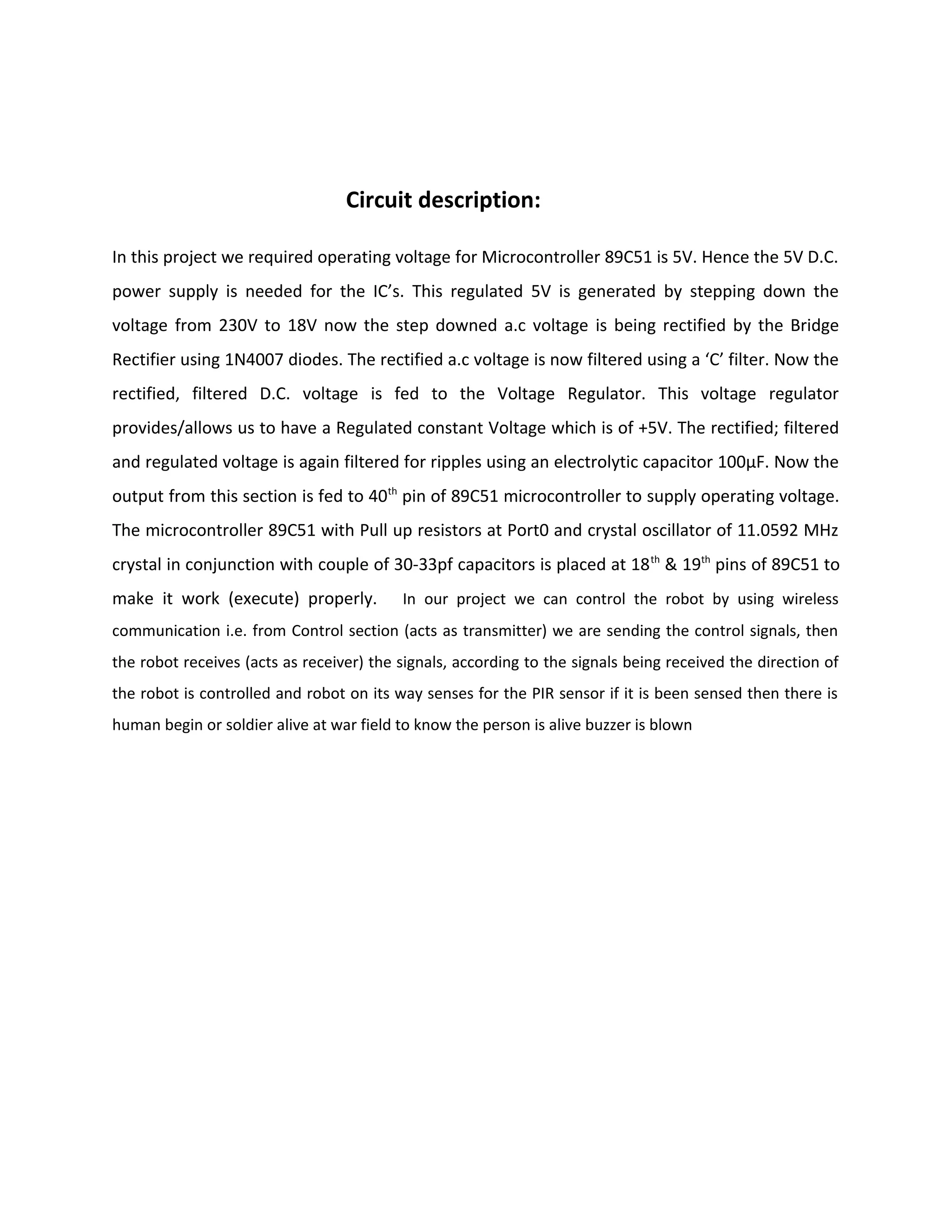
Power supply
The power supplies are designed to convert high voltage AC mains
electricity to a suitable low voltage supply for electronics circuits and other devices. A power
supply can by broken down into a series of blocks, each of which performs a particular function.
A d.c power supply which maintains the output voltage constant irrespective of a.c mains
fluctuations or load variations is known as “Regulated D.C Power Supply”
For example a 5V regulated power supply system as shown below:](https://image.slidesharecdn.com/12-130806042257-phpapp02/75/12-automatic-toll-gate-billing-system-using-rfid-78-2048.jpg)


This document describes an automatic toll gate billing system using RFID technology. The key components of the system include a microcontroller, power supply, RFID reader, smart card reader, MAX232 IC, LCD display, and EEPROM. The system works by reading information from an RFID tag on a vehicle using the RFID reader. It verifies if the person is authorized and deducts the toll amount from their smart card depending on vehicle type. If unauthorized or insufficient funds, a false indication is displayed. The microcontroller controls the overall system operation.


![[IJET-V1I4P5] Authors :Divya Lakshmi M , Dr. Ramesh R](https://cdn.slidesharecdn.com/ss_thumbnails/ijet-v1i4p5-150728164001-lva1-app6892-thumbnail.jpg?width=640&height=640&fit=bounds)


