The microcontroller CPU has a 12-bit instruction set with 3 types of instructions encoded differently. It contains registers like the program counter, accumulator, and status register. The CPU uses a program memory to store instructions and a data memory for operands. It executes instructions in 3 stages - fetch, decode, execute. In each stage, control signals determine which components are enabled to perform operations like fetching instructions, reading operands, and executing ALU operations.


![Each instruction needs 3 clock cycles to finish, i.e. FETCH stage, DECODE stage, and
EXECUTE stage. Note that it is not pipelined. Together with the initial LOAD state, it can be
considered as an FSM of 3 states (technically 4 states).
States:
1. LOAD (initial state): load program to program memory, which takes 1 cycle per instruction
loaded;
2. FETCH (first cycle): fetch current instruction from program memory;
3. DECODE (second cycle): decode instruction to generate control logic, read data memory
for operand;
4. EXECUTE (of the third cycle): execute instruction
Transitions:
1. LOAD → FETCH (initialization finish):
a. Clear content of PC, IR, DR, Acc, SR; DMem is not required to be
cleared.
2. FETCH → DECODE (rising edge of second cycle) :
. IR = PMem [ PC ]
3. DECODE → EXECUTE
. DR = DMem [ IR[3:0] ];
4. EXECUTE → FETCH (rising edge of first cycle and fourth cycle)
. For non-branch instruction, PC = PC + 1; for branch instruction, if
branch is taken, PC = IR [7:0], otherwise PC = PC + 1;
a. For ALU instruction, if the result destination is accumulator, Acc =
ALU.Out; if the result destination is data memory, DMem [ IR[3:0] ] =
ALU.Out.
b. For ALU instruction, SR = ALU.Status;](https://image.slidesharecdn.com/designofmicrocontrollercpu-230921041750-887073c2/75/Design-of-microcontroller-CPU-pdf-10-2048.jpg)
![The transitions can be simplified using enable port of corresponding registers, e.g. assign
ALU.Out to Acc at every clock rising edge if Acc.E is set to 1. Such control signals as Acc.E
are generated as a boolean function of both current state and the current instruction.
Components
Registers
The microcontroller has 3 programmer visible register:
1. Program Counter (8 bit, denoted as PC): contains the index of current
executing instruction.
2. Accumulator (8 bit, denoted as Acc): holds result and 1 operand of the
arithmetic or logic calculation.
3. Status Register (4 bit, denoted as SR): holds 4 status bit, i.e. Z, C, S, O.
a. Z (zero flag, SR[3]): 1 if result is zero, 0 otherwise.
b. C (carry flag, SR[2]): 1 if carry is generated, 0 otherwise.
c. S (sign flag, SR[1]): 1 if result is negative (as 2’s complement), 0
otherwise.
d. O (overflow flag, SR[0]): 1 if result generates overflow, 0 otherwise.
Each of these registers has an enable port, as a flag for whether the value of the register should
be updated in state transition. They are denoted as PC.E, Acc.E, and SR.E.
The microcontroller has 2 programmer invisible registers (i.e. they can not be manipulated by
programmer):
1. Instruction Register (12 bit, denoted as IR): contains the current executing
instruction.
2. Data Register (8 bit, denoted as DR): contains the operand read from data
memory.
Similarly, each of these registers has an enable port as a flag for whether the value of the
register should be updated in state transition. They are denoted as IR.E and DR.E.
Program memory
The microcontroller has a 256 entry program memory that stores program instructions, denoted
as PMem. Each entry is 12 bits, the ith entry is denoted as PMem[i]. The program memory has
the following input/output ports.
• Enable port (1 bit, input, denoted as PMem.E): enable the device, i.e. if it is 1,
then the entry specified by the address port will be read out, otherwise, nothing is read
out.
• Address port (8 bit, input, denoted as PMem.Addr): specify which instruction
entry is read out, connected to PC.
• Instruction port (12 bit, output, denoted as PMem.I): the instruction entry that
is read out, connected to IR.
• 3 special ports are used to load program to the memory, not used for executing
instructions.](https://image.slidesharecdn.com/designofmicrocontrollercpu-230921041750-887073c2/75/Design-of-microcontroller-CPU-pdf-11-2048.jpg)
![• Load enable port (1 bit, input, denoted as PMem.LE): enable the load, i.e. if it
is 1, then the entry specified by the address port will be load with the value specified
by the load instruction input port and the instruction port is supplied with the same
value; otherwise, the entry specified by the address port will be read out on instruction
port, and value on instruction load port is ignored.
• Load address port (8 bit, input, denoted as PMem.LA): specify which
instruction entry is loaded.
• Load instruction port (12 bit, input, denoted as PMem.LI): the instruction that
is loaded.
For example, if the address point is supplied with 8’b0000_0011 and enable is set to 1, the
fourth entry is read out on instruction port.
Note that program load only takes effect on clock rising edge, while instruction read out
happens all the time.
Data memory
The microcontroller has a 16 entry data memory, denoted as DMem. Each entry is 8 bits, the
ith entry is denoted as DMem[i]. The program memory has the following input/output ports.
• Enable port (1 bit, input, denoted as DMem.E): enable the device, i.e. if it is 1,
then the entry specified by the address port will be read out or written in; otherwise
nothing is read out or written in.
• Write enable port(1 bit, input, denoted as DMem.WE): enable the write, i.e.
if it is 1, then the entry specified by the address port will be written with the value
specified by the data input port and the data output port is supplied with the same value;
otherwise, the entry specified by the address port will be read out on data output port,
and value on data input port is ignored.
• Address port (4 bit, input, denoted as DMem.Addr): specify which data
entry is read out, connected to IR[3:0].
• Data input port (8 bit, input, denoted as DMem.DI): the value that is written
in, connected to ALU.Out.
• Data output port (8 bit, output, denoted as DMem.DO): the data entry that
is read out, connected to MUX2.In1.
For example, if the address point is supplied with 8’0000_0011, data input port is supplied with
8’0000_0000, enable is set to 1, and write enable is set to 1, the fourth entry of the data memory
is written with value 0 and the data output port shows 8’0000_0000.
As another example, if the address point is supplied with 8’0000_0011, data input port is
supplied with 8’0000_0000, enable is set to 1, while write enable is set to 0, the fourth entry of
the data memory is read out on data output port.
Note that write only takes effect on clock rising edge, while read happens all the time, similar
to program memory.
PC adder
PC adder is used to add PC by 1, i.e. move to the next instruction. This component is pure
combinational. It has the following port.
• Adder input port (8 bit, input, denoted as Adder.In): connected to PC.](https://image.slidesharecdn.com/designofmicrocontrollercpu-230921041750-887073c2/75/Design-of-microcontroller-CPU-pdf-12-2048.jpg)
![• Adder output port (8 bit, output, denoted as Adder.Out): connected to
MUX1.In2.
MUX1
MUX1 is used to choose the source for updating PC. If the current instruction is not a branch
or it is a branch but the branch is not taken, PC is incremented by 1; otherwise PC is set to the
jumping target, i.e. IR [7:0]. It has the following port.
• MUX1 input 1 port (8 bit, input, denoted as MUX1.In1): connected to IR [7:0].
• MUX1 input 2 port (8 bit, input, denoted as MUX1.In2): connected to
Adder.Out.
• MUX1 selection port (1 bit, input, denoted as MUX1.Sel): connected to control
logic.
• MUX1 output port (8 bit, output, denoted as MUX1.Out): connected to PC.
ALU
ALU is used to do the actual computation for the current instruction. This component is pure
combinational. It has the following port. The mode of ALU is listed in the following table.
• ALU operand 1 port (8 bit, input, denoted as ALU.Operand1): connected to
Acc.
• ALU operand 2 port (8 bit, input, denoted as ALU.Operand2): connected to
MUX2.Out.
• ALU enable port (1 bit, input, denoted as ALU.E): connected to control logic.
• ALU mode port (4 bit, input, denoted as ALU.Mode): connected to control
logic.
• Current flags port (4 bit, input, denoted as ALU.CFlags): connected to SR.
• ALU output port (8 bit, output, denoted as ALU.Out): connected to DMem.DI.
• ALU flags port (4 bit, output, denoted as ALU.Flags): the Z (zero), C (carry),
S (sign), O (overflow) bits, from MSB to LSB, connected to status register.](https://image.slidesharecdn.com/designofmicrocontrollercpu-230921041750-887073c2/75/Design-of-microcontroller-CPU-pdf-13-2048.jpg)
![MUX2
MUX2 is used to choose the source for operand 2 of ALU. If the current instruction is M type,
operand 2 of ALU comes from data memory; if the current instruction is I type, operand 2 of
ALU comes from the instruction, i.e. IR [7:0]. It has the following port.
• MUX2 input 1 port (8 bit, input, denoted as MUX2.In1): connected to IR [7:0].
• MUX2 input 2 port (8 bit, input, denoted as MUX2.In2): connected to DR.
• MUX2 selection port (1 bit, input, denoted as MUX2.Sel): connected to control
logic.
• MUX2 output port (8 bit, output, denoted as MUX2.Out): connected to
ALU.Operand2.
Control unit design
Control signal is derived from the current state and current instruction. The control logic
component is purely combinational. There are in total 12 control signals, listed as follows.
• PC.E: enable port of program counter (PC);
• Acc.E: enable port of accumulator (Acc);
• SR.E: enable port of status register (SR);](https://image.slidesharecdn.com/designofmicrocontrollercpu-230921041750-887073c2/75/Design-of-microcontroller-CPU-pdf-14-2048.jpg)
![• IR.E: enable port of instruction register (IR);
• DR.E: enable port of data register (DR);
• PMem.E: enable port of program memory (PMem);
• DMem.E: enable port of data memory (DMem);
• DMem.WE: write enable port of data memory (DMem);
• ALU.E: enable port of ALU;
• ALU.Mode: mode selection port of ALU;
• MUX1.Sel: selection port of MUX1;
• MUX2.Sel: selection port of MUX2;
The following table documents the detail of how these control signals are generated important
signals are marked in red.
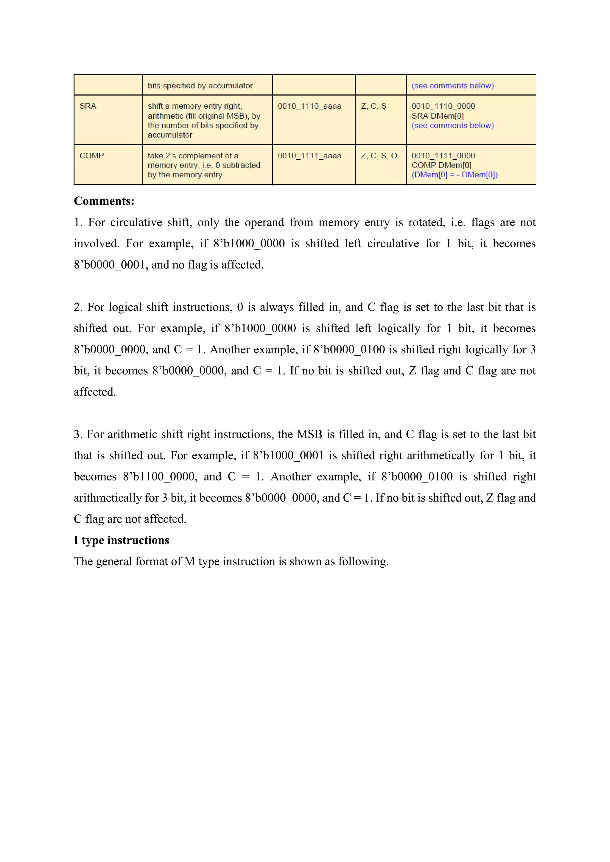
Comments:
1. Note that in EXECUTE state of conditional branch instructions, the value of MUX1.Sel is
actually SR[ IR [9:8] ];
2. Note that in EXECUTE stage of ALU I type instruction, the value of ALU.Mode is actually
{0, IR[10:8]}. In the table above, 0 extension is assumed.
3. Be careful that PMem.LE is not shown in this table. If the processor is not in LOAD state,
PMem.LE is always set to 0.](https://image.slidesharecdn.com/designofmicrocontrollercpu-230921041750-887073c2/75/Design-of-microcontroller-CPU-pdf-15-2048.jpg)
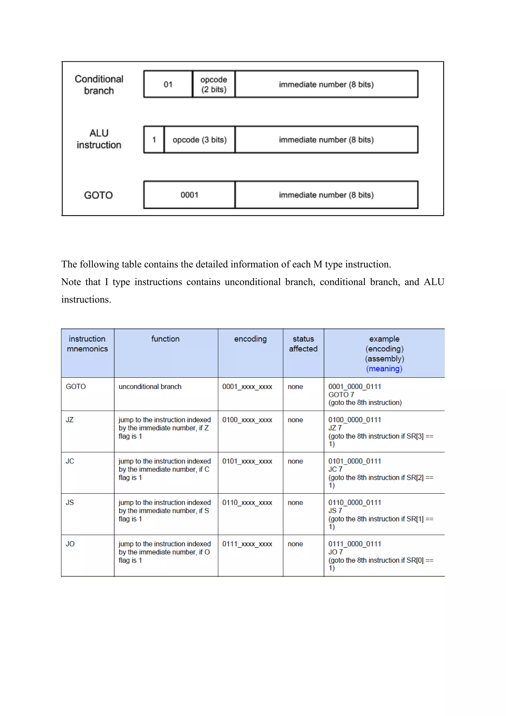
![The type and category of instruction can be identified by the first 4 bits of the instruction, i.e.
IR[11:8], as denoted in the first column of the above table.
Besides, when loading the program, the control signal is generated as below.
If the processor is in LOAD state, PMem.LE is always set to 1.
First is the Verilog code for ALU unit:
// fpga4student.com: FPGA project, Verilog project, VHDL project
// Verilog project: Verilog code for Microcontroller
// Verilog code for ALU
module ALU( input [7:0] Operand1,Operand2,
input E,
input [3:0] Mode,
input [3:0] CFlags,
output [7:0] Out,
output [3:0] Flags
// the Z (zero), C (carry), S (sign),O (overflow) bits, from MSB to LSB, connected to status
register
);
wire Z,S,O;
reg CarryOut;
reg [7:0] Out_ALU;
always @(*)
begin
case(Mode)
4'b0000: {CarryOut,Out_ALU} = Operand1 + Operand2;
4'b0001: begin Out_ALU = Operand1 - Operand2;
CarryOut = !Out_ALU[7];
end
4'b0010: Out_ALU = Operand1;
4'b0011: Out_ALU = Operand2;
4'b0100: Out_ALU = Operand1 & Operand2;
4'b0101: Out_ALU = Operand1 | Operand2;
4'b0110: Out_ALU = Operand1 ^ Operand2;
4'b0111: begin
Out_ALU = Operand2 - Operand1;](https://image.slidesharecdn.com/designofmicrocontrollercpu-230921041750-887073c2/75/Design-of-microcontroller-CPU-pdf-16-2048.jpg)
![CarryOut = !Out_ALU[7];
end
4'b1000: {CarryOut,Out_ALU} = Operand2 + 8'h1;
4'b1001: begin
Out_ALU = Operand2 - 8'h1;
CarryOut = !Out_ALU[7];
end
4'b1010: Out_ALU = (Operand2 << Operand1[2:0])| ( Operand2 >> Operand1[2:0]);
4'b1011: Out_ALU = (Operand2 >> Operand1[2:0])| ( Operand2 << Operand1[2:0]);
4'b1100: Out_ALU = Operand2 << Operand1[2:0];
4'b1101: Out_ALU = Operand2 >> Operand1[2:0];
4'b1110: Out_ALU = Operand2 >>> Operand1[2:0];
4'b1111: begin
Out_ALU = 8'h0 - Operand2;
CarryOut = !Out_ALU[7];
end
default: Out_ALU = Operand2;
endcase
end
assign O = Out_ALU[7] ^ Out_ALU[6];
assign Z = (Out_ALU == 0)? 1'b1 : 1'b0;
assign S = Out_ALU[7];
assign Flags = {Z,CarryOut,S,O};
assign Out = Out_ALU;
// fpga4student.com: FPGA project, Verilog project, VHDL project
endmodule
Next is the Verilog code for data memory:
// fpga4student.com: FPGA project, Verilog project, VHDL project
// Verilog project: Verilog code for Microcontroller
// Verilog code for data memory
module DMem( input clk,
input E, // Enable port
input WE, // Write enable port
input [3:0] Addr, // Address port
input [7:0] DI, // Data input port
output [7:0] DO // Data output port
);
reg [7:0] data_mem [255:0];
// fpga4student.com: FPGA project, Verilog project, VHDL project
always @(posedge clk)](https://image.slidesharecdn.com/designofmicrocontrollercpu-230921041750-887073c2/75/Design-of-microcontroller-CPU-pdf-17-2048.jpg)
![begin
if(E==1 && WE ==1)
data_mem[Addr] <= DI;
end
assign DO = (E ==1 )? data_mem[Addr]:0;
endmodule
Verilog code for adder and MUX1:
// Verilog project: Verilog code for microcontroller
// Submodule: Verilog code for Adder and MUXs
module adder( input [7:0] In,
output [7:0] Out
);
assign Out = In + 1;
endmodule
module MUX1( input [7:0] In1,In2,
input Sel,
output [7:0] Out
);
assign Out = (Sel==1)? In1: In2;
endmodule
Continue on the Verilog code for program memory:
// Verilog project: Verilog code for microcontroller
// Submodule: Verilog code for Adder and MUXs// fpga4student.com: FPGA project, Verilog
project, VHDL project
// Verilog project: Verilog code for microcontroller
module PMem( input clk,
input E, // Enable port
input [7:0] Addr, // Address port
output [11:0] I, // Instruction port
// 3 special ports are used to load program to the memory
input LE, // Load enable port
input[7:0] LA, // Load address port
input [11:0] LI//Load instruction port
);
reg [11:0] Prog_Mem[255:0] ;
// fpga4student.com: FPGA project, Verilog project, VHDL project
always @(posedge clk)](https://image.slidesharecdn.com/designofmicrocontrollercpu-230921041750-887073c2/75/Design-of-microcontroller-CPU-pdf-18-2048.jpg)
![begin
if(LE == 1) begin
Prog_Mem[LA] <= LI;
end
end
assign I = (E == 1) ? Prog_Mem[Addr]: 0 ;
endmodule
module adder( input [7:0] In,
output [7:0] Out
);
assign Out = In + 1;
endmodule
module MUX1( input [7:0] In1,In2,
input Sel,
output [7:0] Out
);
assign Out = (Sel==1)? In1: In2;
endmodule
Next, the Verilog code for Control unit:
// fpga4student.com: FPGA project, Verilog project, VHDL project
// Verilog project: Verilog code for microcontroller
// Control unit in Verilog
module Control_Logic( input[1:0] stage,
input [11:0] IR,
input [3:0] SR,
output reg
PC_E,Acc_E,SR_E,IR_E,DR_E,PMem_E,DMem_E,DMem_WE,ALU_E,MUX1_Sel,M
UX2_Sel,PMem_LE,
output reg [3:0] ALU_Mode
);
parameter LOAD = 2'b00,FETCH = 2'b01, DECODE = 2'b10, EXECUTE = 2'b11;
always @(*)
begin
PMem_LE = 0;
PC_E = 0;
Acc_E = 0;
SR_E = 0;](https://image.slidesharecdn.com/designofmicrocontrollercpu-230921041750-887073c2/75/Design-of-microcontroller-CPU-pdf-19-2048.jpg)
![IR_E = 0;
DR_E = 0;
PMem_E = 0;
DMem_E = 0;
DMem_WE = 0;
ALU_E =0;
ALU_Mode = 4'd0;
MUX1_Sel = 0;
MUX2_Sel = 0;
if(stage== LOAD )
begin
PMem_LE = 1;
PMem_E = 1;
end
else if(stage== FETCH ) begin
IR_E = 1;
PMem_E = 1;
end
else if(stage== DECODE ) begin
if( IR[11:9] == 3'b001)
begin
DR_E = 1;
DMem_E = 1;
end
else
begin
DR_E = 0;
DMem_E = 0;
end
end
else if(stage== EXECUTE )
begin
if(IR[11]==1) begin // ALU I-type
PC_E = 1;
Acc_E = 1;
SR_E = 1;
ALU_E = 1;
ALU_Mode = IR[10:8];
MUX1_Sel = 1;
MUX2_Sel = 0;](https://image.slidesharecdn.com/designofmicrocontrollercpu-230921041750-887073c2/75/Design-of-microcontroller-CPU-pdf-20-2048.jpg)
![end
else if(IR[10]==1) // JZ, JC,JS, JO
begin
PC_E = 1;
MUX1_Sel = SR[IR[9:8]];
end
else if(IR[9]==1)
begin
PC_E = 1;
Acc_E = IR[8];
SR_E = 1;
DMem_E = !IR[8];
DMem_WE = !IR[8];
ALU_E = 1;
ALU_Mode = IR[7:4];
MUX1_Sel = 1;
MUX2_Sel = 1;
end
else if(IR[8]==0)
begin
PC_E = 1;
MUX1_Sel = 1;
end
else
begin
PC_E = 1;
MUX1_Sel = 0;
end
end
end
endmodule
Finally, the Verilog code for microcontroller:
// The microcontroller (similar to Microchip PIC12, simplified extensively, not
compatible in
// instruction set) in this project is a 3 cycle nonpipeline
// 8 bit Harvard structure microcontroller, illustrated as the following block diagram
// fpga4student.com: FPGA project, Verilog project, VHDL project
// Verilog project: Verilog code for microcontroller
module MicroController(input clk,rst
);](https://image.slidesharecdn.com/designofmicrocontrollercpu-230921041750-887073c2/75/Design-of-microcontroller-CPU-pdf-21-2048.jpg)
![parameter LOAD = 2'b00,FETCH = 2'b01, DECODE = 2'b10, EXECUTE = 2'b11;
reg [1:0] current_state,next_state;
reg [11:0] program_mem[9:0];
reg load_done;
reg[7:0] load_addr;
wire[11:0] load_instr;
reg[7:0] PC, DR, Acc;
reg [11:0] IR;
reg [3:0] SR;
wire PC_E,Acc_E,SR_E,DR_E,IR_E;
reg PC_clr,Acc_clr,SR_clr,DR_clr,IR_clr;
wire [7:0] PC_updated,DR_updated;
wire[11:0] IR_updated;
wire[3:0] SR_updated;
wire PMem_E,DMem_E,DMem_WE,ALU_E,PMem_LE,MUX1_Sel,MUX2_Sel;
wire [3:0] ALU_Mode;
wire [7:0] Adder_Out;
wire [7:0] ALU_Out,ALU_Oper2;
// LOAD instruction memory
initial
begin
$readmemb("program_mem.dat", program_mem,0,9);
end
// ALU
ALU ALU_unit( .Operand1(Acc),
.Operand2(ALU_Oper2),
.E(ALU_E),
.Mode(ALU_Mode),
.CFlags(SR),
.Out(ALU_Out),
.Flags(SR_updated) // the Z (zero), C (carry), S (sign),O (overflow) bits, from MSB to
LSB, connected to status register
);
// MUX2
MUX1 MUX2_unit( .In2(IR[7:0]),.In1(DR),
.Sel(MUX2_Sel),
.Out(ALU_Oper2)
);
// Data Memory
DMem DMem_unit( .clk(clk),](https://image.slidesharecdn.com/designofmicrocontrollercpu-230921041750-887073c2/75/Design-of-microcontroller-CPU-pdf-22-2048.jpg)
![.E(DMem_E), // Enable port
.WE(DMem_WE), // Write enable port
.Addr(IR[3:0]), // Address port
.DI(ALU_Out), // Data input port
.DO(DR_updated) // Data output port
);
// Program memory
PMem PMem_unit( .clk(clk),
.E(PMem_E), // Enable port
.Addr(PC), // Address port
.I(IR_updated), // Instruction port
// 3 special ports are used to load program to the memory
.LE(PMem_LE), // Load enable port
.LA(load_addr), // Load address port
.LI(load_instr)//Load instruction port
);
// PC ADder
adder PC_Adder_unit( .In(PC),
.Out(Adder_Out)
);
// fpga4student.com: FPGA project, Verilog project, VHDL project
// MUX1
MUX1 MUX1_unit( .In2(IR[7:0]),.In1(Adder_Out),
.Sel(MUX1_Sel),
.Out(PC_updated)
);
// Control logic
Control_Logic Control_Logic_Unit( .stage(current_state),
.IR(IR),
.SR(SR),
.PC_E(PC_E),
.Acc_E(Acc_E),
.SR_E(SR_E),
.IR_E(IR_E),
.DR_E(DR_E),
.PMem_E(PMem_E),
.DMem_E(DMem_E),
.DMem_WE(DMem_WE),
.ALU_E(ALU_E),
.MUX1_Sel(MUX1_Sel),](https://image.slidesharecdn.com/designofmicrocontrollercpu-230921041750-887073c2/75/Design-of-microcontroller-CPU-pdf-23-2048.jpg)
![.MUX2_Sel(MUX2_Sel),
.PMem_LE(PMem_LE),
.ALU_Mode(ALU_Mode)
);
// fpga4student.com: FPGA project, Verilog project, VHDL project
// LOAD
always @(posedge clk)
begin
if(rst==1) begin
load_addr <= 0;
load_done <= 1'b0;
end
else if(PMem_LE==1)
begin
load_addr <= load_addr + 8'd1;
if(load_addr == 8'd9)
begin
load_addr <= 8'd0;
load_done <= 1'b1;
end
else
begin
load_done <= 1'b0;
end
end
end
// fpga4student.com: FPGA project, Verilog project, VHDL project
assign load_instr = program_mem[load_addr];
// next state
always @(posedge clk)
begin
if(rst==1)
current_state <= LOAD;
else
current_state <= next_state;
end
always @(*)
begin
PC_clr = 0;
Acc_clr = 0;](https://image.slidesharecdn.com/designofmicrocontrollercpu-230921041750-887073c2/75/Design-of-microcontroller-CPU-pdf-24-2048.jpg)