Adcmt catalog 6253-e-denkei DC Voltage Current Source Monitor

ADCMT DC Voltage Current Source Monitor 6253 Best for development or evaluation of high-precision electronic components by wide source range and 6½-digit measurement resolution The DC voltage current source/monitor 6253 is suitable as power source for evaluation of semiconductors and other electronic components and as power source of characteristic systems. In addition to high accuracy, high stability and low noise of our strengths, the 6253 realizes higher precision features such as 5½ digit source resolution, 6½-digit measurement resolution and basis accuracy of ±0.02 %. Furthermore, the 6253 can support various applications by the sweep functions, high-speed pulse source function with a minimum pulse width of 25 μs, the variable integration function and the newly adopted variable slew rate function. https://www.n-denkei.com/singapore/inquiry/

Recommended
More Related Content
What's hot
What's hot (19)
Similar to Adcmt catalog 6253-e-denkei DC Voltage Current Source Monitor
Similar to Adcmt catalog 6253-e-denkei DC Voltage Current Source Monitor (20)
More from NIHON DENKEI SINGAPORE
More from NIHON DENKEI SINGAPORE (20)
Recently uploaded
Recently uploaded (20)
Adcmt catalog 6253-e-denkei DC Voltage Current Source Monitor
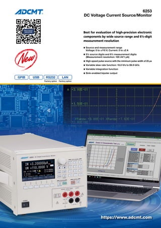
- 1. 6253 DC Voltage Current Source/Monitor Best for evaluation of high-precision electronic components by wide source range and 6½-digit measurement resolution l Source and measurement range Voltage: 0 to ±110 V, Current: 0 to ±2 A l 5½ source digits and 6½ measurement digits (Measurement resolution: 100 nV/1 pA) l High-speed pulse source with the minimum pulse width of 25 μs l Variable slew rate function: 10.0 V/s to 99.9 kV/s l Variable integration function l Sink-enabled bipolar output https://www.adcmt.com RS232 Factory option Factory option
- 2. DC Voltage Current Source/Monitor 2 Source voltage (VS), source current (IS), limit values (HL/LL), measured voltage (VM) and measurement current (IM) are displayed. Voltage and current can be measured simul- taneously. Time settings are important for pulse or sweep source. The time setting screen on the 6253 allows you to make these settings easier than the former models. You can easily view measurement results from the graphically displayed measurement memory data. There are two display options: voltage and current value display and display of the num- ber of memories and measured values. Voltage source (VS), current source (IS), voltage measurement (VM), current measurement (IM) and resistance measurement (RM) can be selected by specifying the source and measurement functions. The 6253 is equipped with A/D twin converters, allowing parallel mea- surement of voltage and current. l Source and measurement range ±2 A at ±32 V ±1 A at ±64 V ±0.5 A at ±110 V l Sink-enabled bipolar output IS IM DRIVING GUARD HI OUTPUT HI SENSE LO SENSE LO OUTPUT VS VM High-resolution and high-throughput source monitor with 5½ source digits and 6½ measurement digits +2 A +1 A +0.5 A +110 V −110 V −64 V +64 V −32 V +32 V -0.5 A -1 A -2 A -Sink -Source +Source +Sink *The operating temperature environment is limited at sink. Display Screen Source and Measurement Functions Time Setting Screen Graph Display Screen Output Range The DC voltage current source/monitor 6253 can be widely used as power supply for evaluating semiconductors and electronic components in research and development and as power supply for characteristic evaluation systems. In addition to high-accuracy, high-stability and low-noise performances of our strengths, the 6253 realizes higher pre- cision features such as 5½-digit source resolution, 6½-digit measurement resolution and basic accuracy of ±0.02 %. Furthermore, the 6253 can support various applications by the sweep functions, high-speed pulse measurement func- tion with a minimum pulse width of 25 μs, the variable in- tegration function and the newly adopted variable slew rate function. USB and GPIB interfaces are mounted as standard, and LAN and RS232 interfaces are available optionally.
- 3. Advantageous Features 3 There are four voltage or current source modes: DC, pulse, DC sweep, pulse sweep. Then, the sweep modes are classified into five sweep types: fixed sweep, linear sweep, log sweep, random sweep (arbitrary waveform generation by user programming), multi-slope linear sweep (linear sweep with four selectable step values). In voltage or current source, the HI/LO limit settings are very im- portant. The 6253 has a function that can set the HI and LO limits individually. In addition, for the voltage limit, both HI and LO limits can be set homo-polar. This prevents capacitors or batteries from be- ing over-discharged. Also, it is suitable for evaluating devices such as LDs that are used at a constant current and do not tolerate reverse voltage application. The rising time and the falling time can be set freely in four ranges. (Variable slew rate) 10.0 to 99.9 V/s, 100 to 999 V/s 1.00 to 9.99 kV/s, 10.0 to 99.9 kV/s The 6253 can select from three output OFF statuses; STBY (output relay OFF), HiZ (output relay ON and high resistance), and LoZ (out- put relay ON and low resistance). Consequently, unnecessary relay ON/OFF operations can be omitted. Using this function will prevent throughput reduction due to relay operating time, and extend relay lifetime dramatically, increasing product reliability. In addition, the setting of a suspend voltage (voltage in HiZ and LoZ status) can prevent transient current from being generated when con- necting voltage sourcing devices such as batteries. OPERATE Vsus 0V LO VL (Conventional) LO VL HI VL CV CC CV CC Charge Discharge Caution! For IS, applying external voltage above the voltage limit will set overload. DC Continuous spot Fixed sweep Linear sweep Random sweep Multi-slope linear sweep Log sweep PULSE Output OFF status Output relay Output status Current limit setting value LoZ ON Vsus, low resistance VS: Setting current limit (IL) IS: 3000 digits in the setting current range (10000 digits for the 3 μA range) HiZ ON Vsus, high resistance 100 nA STBY OFF Open − Variable SR OFF Variable SR ON Voltage/Current Source Mode Variable Slew Rate (SR) Function HI/LO Limit Separate Setting High-Speed Response Suspend Function The output response of the 6253 can be switched between Fast and Slow. When the output response is set to Fast, the 6253 starts up faster than the former models. 200 μs 700 μs 100 V 100 V 6253 Former models
- 4. Various Applications 4 Average Current Measurement [Variable Integration Function] The 6253 allows you to set the integration time arbitrarily from 100 μs to 1000 ms. This makes it measure easily the average current con- sumption of mobile phones and LCDs. As any integration time of the AD converter itself can be set and analog integration is adopted, there are no omissions in waveforms differently from digital integration, resulting in precise average mea- surement. Protection of Overshoot at Capacitive Load When a capacitive load is connected, overshoot occurs at the rising or falling edge and the DUT may be damaged or the output becomes unstable. Using the variable slew rate (SR) function of the 6253 will alleviate voltage waveforms and protect overshoot. AD conversion (Average value measurement) Integration time Average value Measured waveform IS VF Diode Current pulse sweep ISVM IS VM Current Voltage SYNC OUT ISVM DC/DC TRIGGER VCC/ICC VSIM Input current/output voltage synchronous measurement Io Variable SR OFF Variable SR ON [VF temperature dependence by pulse width change] USB and GPIB as standard Optional LAN and RS232 (factory option) External control signals (BNC connector) For synchronous operation or external device control Square connector of rear output terminals (Connecting plug is supplied) Improved operability with a numeric keypad Safety sockets of front output terminals Diode VF Temperature Dependence Evaluation Pulse current application is effective for power diode characteristic test to avoid the influence of self-heating. By using the current pulse sweep function and voltage measurement in synchronization with pulses, precise VF characteristic test is avail- able even with large current. DC/DC Converter Evaluation The following functions are effective for DC/DC converter characteristic test. l The input current and the output voltage or current can be measured simultaneously by synchronizing two units of the 6253. l ±Source and ±sink by bipolar output The 6253 allows 0 V sink which is unavailable by normal electronic load.
- 5. 5 Current source: Current limit: Vo: Compliance voltage Voltage measurement: (Auto zero: ON, integration time: 1PLC to 200ms) Current measurement: (Auto zero: ON, integration time: 1PLC to 200ms) Resistance measurement: (Auto zero: ON, integration time: 1PLC to 200ms) Vo: Compliance voltage *3: CMV error = (A × Vo/1 V); "source or measurement current" × "source or measurement voltage"/1 V digit value Specifications All accuracy specifications are guaranteed for one year at a temperature of 23 °C ±5 °C and a relative humidity of 85 % or less. Voltage source/measurement range: Current source/measurement range: *1 The measurement resolution with integration time of 5 μs, 10 μs, 100μs and 500μs will be as follows: Resistance measurement range: Voltage limit (compliance) range: Current limit (compliance) range: *2: Where, (Hi limit value – Lo limit value) ≥ 600 digits (2000 digits for 3 μA range) Accuracy: Includes calibration accuracy, 1-day stability, temperature coefficient, and linearity. Voltage source: Voltage limit: Voltage limit additional error: When Hi limit is set negative and Lo limit is set positive, an error of ±0.1% of setting is added. Range Accuracy 1-day stability Temperature coefficient ±(% of setting + V) ±(ppm of setting + V)/°C 300 mV 0.02 + 150 μV 0.008 + 80 μV 15 + 15 μV 3 V 0.02 + 200 μV 0.008 + 100 μV 15 + 30 μV 10 V 0.02 + 600 μV 0.008 + 500 μV 15 + 100 μV 30 V 0.02 + 2 mV 0.008 + 1 mV 15 + 300 μV 100 V 0.02 + 6 mV 0.008 + 5 mV 15 + 1 mV Range Accuracy 1-day stability Temperature coefficient ±(% of setting + V) ±(ppm of setting + V)/°C 300 mV 0.025 + 250 μV 0.01 + 100 μV 15 + 30 μV 3 V 0.025 + 500 μV 0.01 + 300 μV 15 + 50 μV 10 V 0.025 + 5 mV 0.01 + 3 mV 15 + 500 μV 30 V 0.025 + 5 mV 0.01 + 3 mV 15 + 500 μV 100 V 0.025 + 50 mV 0.01 + 20 mV 15 + 2 mV Range Source range Setting resolution Measurement range Measurement resolution*1 300 mV 0 to ±320.000 mV 5 μV 0 to ±320.9999 mV 100 nV 3 V 0 to ±3.20000 V 50 μV 0 to ±3.209999 V 1 μV 10 V 0 to ±10.0000 V 100 μV 0 to ±10.09999 V 10 μV 30 V 0 to ±32.0000 V 500 μV 0 to ±32.09999 V 10 μV 100 V 0 to ±110.000 V 1 mV 0 to ±110.9999 V 100 μV Range Source range Setting resolution Measurement range Measurement resolution*1 3 μA 0 to ±3.20000 μA 50 pA 0 to ±3.209999 μA 1 pA 30 μA 0 to ±32.0000 μA 500 pA 0 to ±32.09999 μA 10 pA 300 μA 0 to ±320.000 μA 5 nA 0 to ±320.9999 μA 100 pA 3 mA 0 to ±3.20000 mA 50 nA 0 to ±3.209999 mA 1 nA 30 mA 0 to ±32.0000 mA 500 nA 0 to ±32.09999 mA 10 nA 300 mA 0 to ±320.000 mA 5 μA 0 to ±320.9999 mA 100 nA 2 A 0 to ±2.00000 A 50 μA 0 to ±2.009999 A 1 μA Integration time 5 μs 10 μs 100 μs 500 μs Measurement resolution (digits) 20 10 4 2 Range Measurement range Measurement resolution Determined by voltage range/ current range calculations 0 Ω to 550 GΩ Minimum 0.05 μΩ Setting range Setting resolution*2 0 V to 320.00 mV 10 μV 320.01 mV to 3.2000 V 100 μV 3.2001 V to 10.000 V 1 mV 10.001 V to 32.000 V 1 mV 32.001 V to 110.00 V 10 mV Setting range Setting resolution*2 0.0010 μA to 3.2000 μA 100 pA 3.2001 μA to 32.000 μA 1 nA 32.001 μA to 320.00 μA 10 nA 320.01 μA to 3.2000 mA 100 nA 3.2001 mA to 32.000 mA 1 μA 32.001 mA to 320.00 mA 10 μA 320.01 mA to 2.0000 A 100 μA Range Accuracy 1-day stability Temperature coefficient ±(% of setting + A + A × Vo/1 V) ±(ppm of setting + A + A × Vo/1 V )/°C 3 μA 0.03 + 500 pA + 30 pA 0.01 + 300 pA + 20 pA 20 + 150 pA + 1 pA 30 μA 0.03 + 4 nA + 300 pA 0.01 + 2.5 nA + 200 pA 20 + 1 nA + 10 pA 300 μA 0.025 + 40 nA + 3 nA 0.01 + 25 nA + 2 nA 20 + 10 nA + 100 pA 3 mA 0.025 + 350 nA + 30 nA 0.008 + 200 nA + 20 nA 20 + 100 nA + 1 nA 30 mA 0.025 + 3.5 μA + 300 nA 0.008 + 2 μA + 200 nA 20 + 1 μA + 10 nA 300 mA 0.03 + 35 μA + 3 μA 0.01 + 20 μA + 2 μA 20 + 10 μA + 100 nA 2 A 0.04 + 350 μA + 30 μA 0.015 + 250 μA + 20 μA 20 + 100 μA + 1 mA Range Accuracy 1-day stability Temperature coefficient ±(% of setting + A + A × Vo/1 V) ±(ppm of setting + A + A × Vo/1 V )/°C 3 μA 0.03 + 1.5 nA + 30 pA 0.01 + 500 pA + 20 pA 20 + 200 pA + 1 pA 30 μA 0.03 + 10 nA + 300 pA 0.01 + 3 nA + 200 pA 20 + 1 nA + 10 pA 300 μA 0.03 + 100 nA + 3 nA 0.01 + 30 nA + 2 nA 20 + 10 nA + 100 pA 3 mA 0.03 + 1 μA + 30 nA 0.01 + 300 nA + 20 nA 20 + 100 nA + 1 nA 30 mA 0.03 + 10 μA + 300 nA 0.01 + 3 μA + 200 nA 20 + 1 μA + 10 nA 300 mA 0.05 + 100 μA + 3 μA 0.015 + 30 μA + 2 μA 20 + 10 μA + 100 nA 2 A 0.06 + 1 mA + 30 μA 0.03 + 300 μA + 20 μA 20 + 100 μA + 1 mA Range Accuracy 1-day stability Temperature coefficient ±(% of reading + V) ±(ppm of reading + V)/°C 300 mV 0.02 + 120 μV 0.006 + 60 μV 15 + 12 μV 3 V 0.02 + 120 μV 0.006 + 80 μV 15 + 15 μV 10 V 0.02 + 500 μV 0.006 + 200 μV 15 + 50 μV 30 V 0.02 + 1.2 mV 0.006 + 800 μV 15 + 150 μV 100 V 0.02 + 5 mV 0.006 + 2 mV 15 + 500 μV Range Accuracy 1-day stability Temperature coefficient ±(% of reading + A + A × Vo/1 V) ±(ppm of reading + A + A × Vo/1 V )/°C 3 μA 0.025 + 500 pA + 30 pA 0.01 + 300 pA + 20 pA 20 + 100 pA + 1 pA 30 μA 0.025 + 4 nA + 300 pA 0.01 + 2.5 nA + 200 pA 20 + 500 pA + 10 pA 300 μA 0.025 + 35 nA + 3 nA 0.01 + 25 nA + 2 nA 20 + 5 nA + 100 pA 3 mA 0.025 + 300 nA + 30 nA 0.01 + 200 nA + 20 nA 20 + 40 nA + 1 nA 30 mA 0.025 + 3 μA + 300 nA 0.01 + 2 μA + 200 nA 20 + 400 nA + 10 nA 300 mA 0.03 + 30 μA + 3 μA 0.01 + 20 μA + 2 μA 20 + 4 μA + 100 nA 2 A 0.04 + 300 μA + 30 μA 0.015 + 250 μA + 20 μA 20 + 40 μA + 1 mA Condition Accuracy ±(% of reading) ±(digits + digits + digits) Voltage source Reading error: (Voltage source setting error + Current measurement reading error) Full-scale error: (Voltage source full-scale error digit value + current measurement full- scale error digit value + CMV error digit value)*3 Current source Reading error: (Current source setting error + Voltage measurement reading error) Full-scale error: (Current source full-scale error digit value + Voltage measurement full- scale error digit value + CMV error digit value)*3
- 6. 6 The full-scale error tolerances listed below are added to the integration time 10 ms to 5 μs and 1-day stability. Source linearity: ±10 digits or less Maximum output current: ±2 A at ±32 V ±1 A at ±64 V ±0.5 A at ±110 V Maximum compliance voltage: ±110 V at ±0.5 A ±64 V at ±1 A ±32 V at ±2 A Output noise: For voltage source, within the range from no load to the maximum load [Vp-p] For current source, at the following load [Ap-p] Voltage source: Current source: Switching noise: *4: The limit operation is inactive. While the limit operation is active, it is the same as the current source range switching noise. *5: “digits” indicates current source values at 5½ digits. Settling time: Time to reach the final value ±0.1% Under the conditions of pure resistance load, load capacitance of 2.5 pF or less, full-scale compliance settings. For voltage source in the 100 V range, the output current should be less than 20 % or less of the limit setting values. Overshoot: ±5 % or less under pure resistance load and at the standard cable end (3 μA, 30 μA and 300 μA ranges excluded) Line regulation: ±0.003% of range or less Load regulation: Voltage source: ±0.003% of range or less (At 4-wire connection under the maximum load) Current source: Depending on the accuracy CMV (A × Vo/1V) Output resistance: At 4-wire connection, not including the output cable Maximum load capacitance: Maximum load capacitance that does not generate oscillation in voltage source or voltage limit status Supplied cable resistance: 100 mΩ or less Maximum inductive load: Maximum inductive load that does not generate oscillation in current source or current limit status Effective CMRR: At unbalanced impedance 1kΩ In DC and at AC 50/60 Hz ± 0.08% NMRR: At AC 50/60 Hz ± 0.08% Measurement range Integration time Unit: digits (at 6 ½ digit display) 10 ms 1 ms 500 μs 100 μs 10 μs 5 μs Voltage measurement 300 mV 150 200 400 600 8000 10000 3 V 50 100 200 300 5000 8000 10 V 50 100 200 300 5000 8000 30 V 50 100 200 300 5000 8000 100 V 50 100 200 300 5000 8000 Current measurement 3 μA 600 1000 1500 2000 5000 10000 30 μA 200 300 300 300 5000 10000 300 μA 100 100 200 300 5000 8000 3 mA 100 100 200 300 5000 8000 30 mA 100 100 200 300 5000 8000 300 mA 100 100 200 300 5000 8000 2 A 100 100 200 300 5000 8000 Range Load resistance Low frequency noise High frequency noise DC to 100 Hz DC to 10 kHz DC to 20 MHz 300 mV - 60 μV 300 μV 5 mV 3 V - 100 μV 400 μV 5 mV 10 V - 1 mV 3 mV 6 mV 30 V - 1 mV 3 mV 6 mV 100 V - 3 mV 5 mV 10 mV Output resistance (Ω) Maximum load capacitance Current range Voltage source Current source 3 μA 3 Ω or less 10 GΩ or higher 1 μF 30 μA 500 mΩ or less 1000 MΩ or higher 1 μF 300 μA 100 mΩ or less 1000 MΩ or higher 1 μF 3 mA 10 mΩ or less 100 MΩ or higher 100 μF 30 mA 10 mΩ or less 10 MΩ or higher 100 μF 300 mA 10 mΩ or less 1 MΩ or higher 2000 μF 2 A 10 mΩ or less 100 kΩ or higher 2000 μF Current source range/ 3 μA, 30 μA 300 μA 3 mA to 2 A current limit range Response Maximum inductive load FAST 100 μH 200 μH 500 μH SLOW 100 μH 500 μH 1 mH Range Load resistance Low frequency noise High frequency noise DC to 100 Hz DC to 10 kHz DC to 20 MHz 3 μA 10 kΩ 10 nA 60 nA 500 nA 30 μA 10 kΩ 10 nA 60 nA 500 nA 300 μA 10 kΩ 30 nA 150 nA 600 nA 3 mA 1 kΩ 200 nA 2 μA 6 μA 30 mA 1 kΩ 2 μA 15 μA 20 μA 300 mA 1 kΩ 20 μA 100 μA 150 μA 2 A 100 Ω 200 μA 1 mA 1.5 mA Typical value [p-p] Load resistance Output ON/OFF noise Voltage source 600 mV At 100 kΩ Current source 600 mV Range switching noise Voltage source 50 mV − Voltage limit 50 mV*4 Voltage measurement 50 mV*4 Current source 700 digits + 50 mV *5 Current measurement Current limit Power OFF noise 600 mV At 100 kΩ (Typical value) Source range Limit range Output response FAST SLOW Voltage source 300 mV 2 A 100 μs 1 ms 3 V 10 V 30 V 200 μs 2 ms 100 V 300 mA 300 μs 3 ms Current source 3 μA 100 V 10 ms 30 μA 5 ms 300 μA 2 ms 5 ms 3 mA 30 mA 800 μs 300 mA 2 A 30 V Integration time 5 μs to 10 ms 1 PLC to 200 ms Current measurement/ voltage measurement 60 dB 120 dB Integration time 5 μs to 10 ms 1 PLC to 200 ms Voltage measurement/ current measurement 0 dB 60 dB
- 7. 7 Interface Function USB interface: USB 2.0 Full-speed, Type B connector GPIB interface: Compliant with IEEE-488.2 Amphenol 24 pin connector Interface function SH1, AH1, T6, L4, SR1, RL1, PP0, DC1, DT1, C0, E2 RS232 interface (factory option): Compliant with EIA232C (RS-232) Baud rate 19200, 9600, 4800, 2400, 1200, 600, 300 Parity EVEN, ODD, NONE Number of data bits 7 bits, 8 bits Number of stop bits 1 bit, 2 bits Dsub 9 pin connector LAN interface (factory option): Compliant with IEEE802.3 10BASE-T, 100BASE-TX RJ-45 connector External control signal: TRIGGER IN SYNC OUT COMPLETE OUT/BUSY IN/BUSY OUT INTERLOCK/OPERATE IN/OPERATE OUT BNC connector Setting Time Minimum pulse width: 25 μs Minimum step (repeat) time: Under fixed source/measurement range, integration time of 5 µs, the minimum measurement or source delay time, calculation function OFF, auto zero OFF, and voltage/current measurement *6: 500 μs when the calculation function is OFF Source delay time: Period (pulse cycle): Pulse width: Measurement delay time: *7: The setting resolution is determined by the period time resolution. Source and Measurement Function DC source and measurement: DC voltage and current source and measurement Pulse source and measurement: Source and measurement of pulse voltage and current (However, measurement auto range in pulse source is impossible.) DC sweep source and measurement: Source and measurement by Linear, Multi-slope linear, Log, Random and Fixed level Pulse sweep source and measurement: Source and measurement by Linear, Multi-slope linear, Log, Random and Fixed level (However, measurement auto range in pulse source is impossible.) Source value monitor: Monitoring source values of DC voltage and current (Measured separately from the measurement function) Integration time: 10 types available: 5 μs, 10 μs, 100μs, 500μs, 1ms, 10ms, 1PLC, 2 PLC, 200 ms and arbitrary value (variable integration) (PLC: Power Line Cycle, 50 Hz: 20 ms, 60 Hz: 16.66 ms) Variable integration setting range: 100 μs to 1000 ms (setting resolution: 100 μs) Sweep mode: Reverse ON (round) / OFF (one way) Sweep repeat count: 1 to 1,000 times or infinite Maximum number of sweep steps: 20,000 steps Maximum random sweep memory: 20,000 data Sampling count: 1 to 20,000 times (Plural samplings done by single trigger) (Valid only in the HOLD status of the DC or pulse mode) Measurement data memory: 20,000 data Measurement auto range: Available only in VSIM or ISVM Measurement function link mode: Links the measurement function to the source function. VSIM or ISVM, ON/OFF available Limit: The HI and LO limits can be set individually. (However, current limits of the same polarity are not allowed.) Calculation function: NULL calculation Comparator calculation (HI, GO, or LO) Scaling calculation MAX, MIN, AVE, TOTAL calculations Trigger style: Auto trigger, External trigger Output terminal: Front safety socket Rear HI OUTPUT, HI SENSE, LO OUTPUT, LO SENSE, DRIVING GUARD Maximum input voltage: 110 V peak (between HI-LO, DG-LO) 3 V peak (between OUTPUT and SENSE) 1 V peak (between HI and DG) 500 V max (between LO and chassis) Maximum remote sensing voltage: ±3 V max HI OUTPUT - HI SENSE, LO OUTPUT - LO SENSE (The voltage between HI SENSE and LO SENSE must be within the maximum output voltage range.) Voltage measurement input resistance: 10 GΩ or higher Voltage measurement input leak current: ±100 pA or lower Setting range Resolution *7 Setting accuracy 0.005 ms to 60.000 ms 1 μs ±(0.1 % + 10 μs) 60.01 ms to 600.00 ms 10 μs 600.1 ms to 6000.0 ms 100 μs 6001 ms to 59997 ms 1 ms Setting range Resolution *7 Setting accuracy 0.025 ms to 60.000 ms 1 μs ±(0.1 % + 10 μs) 60.01 ms to 600.00 ms 10 μs 600.1 ms to 6000.0 ms 100 μs 6001 ms to 59997 ms 1 ms Setting range Resolution *7 Setting accuracy 0.020 ms to 60.000 ms 1 μs ±(0.1 % + 10 μs) 60.01 ms to 600.00 ms 10 μs 600.1 ms to 6000.0 ms 100 μs 6001 ms to 59997 ms 1 ms Setting range Resolution *7 Setting accuracy 0.050 ms to 60.000 ms 1 μs ±(0.1 % + 10 μs) 60.01 ms to 600.00 ms 10 μs 600.1 ms to 6000.0 ms 100 μs 6001 ms to 60000 ms 1 ms Measurement Source mode Memory mode Minimum step time OFF DC, DC sweep OFF, Normal 100 µs Pulse, pulse sweep 125 µs Common mode Burst 50 µs ON DC, pulse Normal 250 µs *6 OFF Sweep Burst 50 μs Normal 250 µs *6 OFF
- 8. Optional accessories *8: Installing a rack or the slide rail set (A02165) is required. The side joint set (A02641) is required. Options Hold time: Auto range delay time: General Specifications Operating environment: Temperature: 0°C to +50°C Relative humidity: 85% or less, no condensation The operating temperature environment is limited at sink. Storage environment: Temperature: -25°C to +70°C Relative humidity: 85% or less, no condensation Warm-up time: 60 minutes or more Display: 4.3-inch color LCD display Power supply: AC power supply 100V/120V/220V/240V (User selectable) Use a power cable and a fuse that are compliant with the safety standard when changing the power supply voltage. Line frequency: 50Hz/60Hz Power consumption: 330 VA or less Dimensions: Approx. 212 (W) x 177 (H) x 450 (D) mm Mass: 15 kg or less Safety: Compliant with IEC61010-1 Ed.3 EMI: EN61326-1 class A Vibration proof: Compliant with IEC60068-2-6 2G Supplied accessories Name Model RS232 interface (factory option) OPT6253+03 LAN interface (factory option) OPT6253+06 Option number Standard OPT. 32 OPT. 42 OPT. 44 Power voltage 100 V 120 V 220 V 240 V Name Model Test fixture 12701A Input cable (1 m) A01041 Input/output cable (red and black safety cable 1m) A01044 Banana tip adapter (red and black) A08531 Alligator clip adapter (red and black) A08532 Input and output cable (banana-banana, 4-wire shielded, 0.5 m) A01047-01 Input and output cable (banana-banana, 4-wire shielded, 1 m) A01047-02 Input and output cable (banana-banana, 4-wire shielded, 1.5 m) A01047-03 Input and output cable (banana-banana, 4-wire shielded, 2 m) A01047-04 Input and output cable (banana-banana, 4-wire shielded with guard, 1 m) A01038-100 Input and output cable (5-pin plug - alligator, 1 m) CC060001-100 Input and output cable (5-pin plug, 2 m) CC060002-200 Input cable (BNC-BNC, 1.5 m) A01036-1500 Rack mount set (JIS 4U single) A02269 Rack mount set (JIS 4U twin)*8 CC022004 Rack mount set (EIA 4U single) A02469 Rack mount set (EIA 4U twin)*8 CC024004 Side joint set (4U) A02641 Slide rail set A02615 Front handle set (4U) CC028004 Name Model Quantity Power cable A01402 1 Input/output cable (red and black safety cable 1m) A01044 1 Banana tip adapter (red and black) A08531 1 Alligator clip adapter (red and black) A08532 1 Output connector (plug) JCS-RB0005JX04 1 Output connector (plug) cover YEE-1000734 1 Cable tie ESM-000257 1 © 2020 ADC CORPORATION Printed in Japan 6253E-NP Aug. '20 A Head Office (R&D Center) East Branch (Sales Dept.) Okabe-building, 3-515, Onari-cho, Omiya-ku, Saitama-shi, Saitama 330-0852, Japan Phone: +81-48-651-4433 Fax: +81-48-651-4432 E-mail : kcc@adcmt.com URL : https://www.adcmt.com 77-1, Miyako Namegawa-machi, Hiki-gun, Saitama 355-0812, Japan Phone: +81-493-56-4433 Fax: +81-493-57-1092 ● Please read through the operation manual carefully before using the product. ● All specifications are subject to change without notice. Setting range Resolution Setting accuracy 0 ms to 6000.0 ms 100 μs ±(2 % + 2 ms) Setting range Resolution Setting accuracy 0 ms to 5000.0 ms 100 μs ±(2 % + 2 ms) https://www.n-denkei.com/singapore/inquiry/