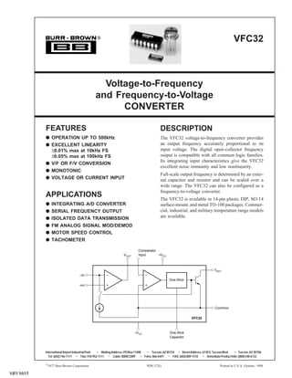
SlideShare a Scribd company logo
1 of 12
Download to read offline
®
VFC32
InternationalAirportIndustrialPark • MailingAddress:POBox11400 • Tucson,AZ85734 • StreetAddress:6730S.TucsonBlvd. • Tucson,AZ 85706
Tel:(602)746-1111 • Twx:910-952-1111 • Cable:BBRCORP • Telex:066-6491 • FAX:(602)889-1510 • ImmediateProductInfo:(800)548-6132
FEATURES
q OPERATION UP TO 500kHz
q EXCELLENT LINEARITY
±0.01% max at 10kHz FS
±0.05% max at 100kHz FS
q V/F OR F/V CONVERSION
q MONOTONIC
q VOLTAGE OR CURRENT INPUT
APPLICATIONS
q INTEGRATING A/D CONVERTER
q SERIAL FREQUENCY OUTPUT
q ISOLATED DATA TRANSMISSION
q FM ANALOG SIGNAL MOD/DEMOD
q MOTOR SPEED CONTROL
q TACHOMETER
DESCRIPTION
The VFC32 voltage-to-frequency converter provides
an output frequency accurately proportional to its
input voltage. The digital open-collector frequency
output is compatible with all common logic families.
Its integrating input characteristics give the VFC32
excellent noise immunity and low nonlinearity.
Full-scale output frequency is determined by an exter-
nal capacitor and resistor and can be scaled over a
wide range. The VFC32 can also be configured as a
frequency-to-voltage converter.
The VFC32 is available in 14-pin plastic DIP, SO-14
surface-mount, and metal TO-100 packages. Commer-
cial, industrial, and military temperature range models
are available.
Voltage-to-Frequency
and Frequency-to-Voltage
CONVERTER
–In
One-Shot
+VCC
fOUT
–VCC
VFC32
Common
+In
Comparator
InputVOUT
One-Shot
Capacitor
©
1977 Burr-Brown Corporation PDS-372G Printed in U.S.A. October, 1998
SBVS015
2VFC32
SPECIFICATIONS
At TA = +25°C and VCC = ±15V, unless otherwise noted.
V Specification the same as VFC32KP.
NOTES: (1) A 25% duty cycle (0.25mA input current) is recommended for best linearity. (2) Adjustable to zero. See Offset and Gain Adjustment section. (3) Linearity error is specified
at any operating frequency from the straight line intersecting 90% of full scale frequency and 0.1% of full scale frequency. See Discussion of Specifications section. Above 200kHz,
it is recommended all grades be operated below +85°C. (4) ±0.015% of FSR for negative inputs shown in Figure 5. Positive inputs are shown in Figure 1. (5) FSR = Full Scale Range
(corresponds to full scale frequency and full scale input voltage). (6) Exclusive of external components’ drift. (7) Positive drift is defined to be increasing frequency with increasing
temperature. (8) For operations above 200kHz up to 500kHz, see Discussion of Specifications and Installation and Operation sections. (9) One pulse of new frequency plus 1µs.
VFC32KP, KU VFC32BM VFC32SM
PARAMETER CONDITIONS MIN TYP MAX MIN TYP MAX MIN TYP MAX UNITS
INPUT (V/F CONVERTER) FOUT = VIN/7.5 R1 C1
Voltage Range(1)
Positive Input >0 +0.25mA V V V V V
x R1
Negative Input >0 –10 V V V V V
Current Range(1) >0 +0.25 V V V V mA
Bias Current
Inverting Input 20 100 V V V V nA
Noninverting Input 100 250 V V V V nA
Offset Voltage(2) 1 4 V V V V mV
Differential Impedance 300 || 10 650 || 10 V V V V kΩ || pF
Common-mode
Impedance 300 || 3 500 || 3 V V V V MΩ || pF
INPUT (F/V CONVERTER) VOUT = 7.5 R1 C1 FIN
Impedance 50 || 10 150 || 10 V V V V kΩ || pF
Logic “1” +1.0 V V V V V
Logic “0” –0.05 V V V V V
Pulse-width Range 0.1 150k/FMAX V V V V µs
ACCURACY
Linearity Error(3) 0.01Hz ≤ Oper
Freq ≤ 10kHz ±0.005 ±0.010(4)
V V V V % of FSR(5)
0.1Hz ≤ Oper
Freq ≤ 100kHz ±0.025 ±0.05 V V V V % of FSR
0.5Hz ≤ Oper
Freq ≤ 500kHz ±0.05 V V % of FSR
Offset Error Input
Offset Votlage(2)
1 4 V V V V mV
Offset Drift(6) ±3 V V ppm of FSR/°C
Gain Error(2)
5 V V % of FSR
Gain Drift(6) f = 10kHz ±75 ±50 ±100 ±70 ±150 ppm/°C
Full Scale Drift f = 10kHz ±75 ±50 ±100 ±70 ±150 ppm of FSR/°C
(offset drift and
gain drift)(6, 7)
Power Supply f = DC, ±VCC = 12VDC
Sensitivity to 18VDC ±0.015 V V % of FSR/%
OUTPUT (V/F CONVERTER) (open collector output)
Voltage, Logic “0” ISINK = 8mA 0 0.2 0.4 V V V V V V V
Leakage Current,
Logic “1” VO = 15V 0.01 1.0 V V V V µA
Voltage, Logic “1” External Pull-up Resistor
Required (see Figure 4) VPU V V V
Pulse Width For Best Linearity 0.25/FMAX V V s
Fall Time IOUT = 5mA, CLOAD = 500pF 400 V V ns
OUTPUT (F/V CONVERTER) VOUT
Voltage IO ≤ 7mA 0 to +10 V V V
Current VO ≤ 7VDC +10 V V mA
Impedance Closed Loop 1 V V Ω
Capacitive Load Without Oscillation 100 V V pF
DYNAMIC RESPONSE
Full Scale Frequency 500(8)
V V kHz
Dynamic Range 6 V V decades
Settling Time (V/F) to Specified Linearity
for a Full Scale Input Step (9) V V
Overload Recovery < 50% Overload (9)
V V
POWER SUPPLY
Rated Voltage ±15 V
Voltage Range ±11 ±20 V V
Quiescent Current ±5.5 ±6.0 V V V mA
TEMPERATURE RANGE
Specification 0 +70 –25 +85 –55 +125 °C
Operating –25 +85 –55 +125 –55 +125 °C
Storage –25 +85 –65 +150 –65 +150 °C
3 VFC32
Supply Voltage ................................................................................... ±22V
Output Sink Current (FOUT) ................................................................ 50mA
Output Current (VOUT
) ...................................................................... +20mA
Input Voltage, –Input ..................................................................... ±Supply
Input Voltage, +Input ..................................................................... ±Supply
Comparator Input .......................................................................... ±Supply
Storage Temperature Range:
VFC32BM, SM ............................................................. –65°C to +150°C
VFC32KP, KU ................................................................ –25°C to +85°C
ABSOLUTE MAXIMUM RATINGS
The information provided herein is believed to be reliable; however, BURR-BROWN assumes no responsibility for inaccuracies or omissions. BURR-BROWN assumes
no responsibility for the use of this information, and all use of such information shall be entirely at the user’s own risk. Prices and specifications are subject to change
without notice. No patent rights or licenses to any of the circuits described herein are implied or granted to any third party. BURR-BROWN does not authorize or warrant
any BURR-BROWN product for use in life support devices and/or systems.
PIN CONFIGURATIONS
Top View
+VCC
1
2
3
4
5
6
7
14
13
12
11
10
9
8
Input
Amp
Switch
One-
shot
NC
NC
–VCC
fOUT
–In
NC
One-Shot
Capacitor
VOUT
Common
+In
NC
NC
Comparator
Input
P Package
U Package
(Epoxy Dual-in-line)
+VCC
Switch
NC
–VCC (Case)
fOUT
+In
One-Shot
Capacitor
Common
–In
Comparator
Input
M Package
(TO-100)
1
3
4
5 6
7
8
9
10
VOUT
NC = no internal connection
External connection permitted.
2
One-
shot
Input Amp
ELECTROSTATIC
DISCHARGE SENSITIVITY
This integrated circuit can be damaged by ESD. Burr-Brown
recommends that all integrated circuits be handled with
appropriate precautions. Failure to observe proper handling and
installation procedures can cause damage.
ESD damage can range from subtle performance degradation to
complete device failure. Precision integrated circuits may be
more susceptible to damage because very small parametric
changes could cause the device not to meet its published specifi-
cations.PACKAGE
DRAWING TEMPERATURE
PRODUCT PACKAGE NUMBER(1) RANGE
VFC32KP 14-Pin Plastic DIP 010 0°C to 70°C
VFC32BM TO-100 Metal 007 –25°C to +85°C
VFC32SM TO-100 Metal 007 –55°C to +125°C
VFC32KU SO-14 SOIC 235 0°C to +70°C
NOTE: (1) For detailed drawing and dimension table, please see end of data
sheet, or Appendix C of Burr-Brown IC Data Book.
PACKAGE/ORDERING INFORMATION
4VFC32
TYPICAL PERFORMANCE CURVES
At TA = +25°C and VCC = ±15V, unless otherwise noted.
1k 1M
Full Scale Frequency (Hz)
0.10
0.001
TypicalLinearityError(%ofFSR)
10k 100k
0.01
TA = +25°C
LINEARITY ERROR vs FULL SCALE FREQUENCY
Duty Cycle = 25%
at Full Scale
0 10k
Operating Frequency (Hz)
1
–1.0
LinearityError(Hz)
1k 7k
0
LINEARITY ERROR vs OPERATING FREQUENCY
2k 3k 4k 5k 6k 8k 9k
0.5
–0.5
fFULL SCALE = 10kHz, 25% Duty Cycle
TA = +25°C
1k 1M
Full Scale Frequency (Hz)
1000
10
FullScaleTempDrift(ppmofFSR/°C)
10k 100k
100 (SM, KP, KU)
FULL SCALE DRIFT vs FULL SCALE FREQUENCY
(BM)
5 VFC32
APPLICATION INFORMATION
Figure 1 shows the basic connection diagram for frequency-
to-voltage conversion. R1 sets the input voltage range. For a
10V full-scale input, a 40kΩ input resistor is recommended.
Other input voltage ranges can be achieved by changing the
value of R1.
R1 should be a metal film type for good stability. Manufac-
turing tolerances can produce approximately ±10% variation
in output frequency. Full-scale output frequency can be
trimmed by adjusting the value of R1—see Figure 3.
The full-scale output frequency is determined by C1. Values
shown in Figure 1 are for a full-scale output frequency of
10kHz. Values for other full-scale frequencies can be read
from Figure 2. Any variation in C1—tolerance, temperature
drift, aging—directly affect the output frequency. Ceramic
NPO or silver-mica types are a good choice.
For full-scale frequencies above 200kHz, use larger capaci-
tor values as indicated in Figure 2, with R1 = 20kΩ.
The value of the integrating capacitor, C2, does not directly
influence the output frequency, but its value must be chosen
within certain bounds. Values chosen from Figure 2 produce
approximately 2.5Vp-p integrator voltage waveform. If C2’s
value is made too low, the integrator output voltage can
exceed its linear output swing, resulting in a nonlinear
response. Using C2 values larger than shown in Figure 2 is
acceptable.
Accuracy or temperature stability of C2 is not critical be-
cause its value does not directly affect the output frequency.
For best linearity, however, C2 should have low leakage and
low dielectric absorption. Polycarbonate and other film
capacitors are generally excellent. Many ceramic types are
adequate, but some low-voltage ceramic capacitor types
may degrade nonlinearity. Electrolytic types are not recom-
mended.
FREQUENCY OUTPUT PIN
The frequency output terminal is an open-collector logic
output. A pull-up resistor is usually connected to a 5V logic
supply to create standard logic-level pulses. It can, however,
be connected to any power supply up to +VCC. Output pulses
have a constant duration and positive-going during the one-
shot period. Current flowing in the open-collector output
transistor returns through the Common terminal. This termi-
nal should be connected to logic ground.
(1)
FIGURE 1. Voltage-to-Frequency Converter Circuit.
fO
VINT
VIN
One-Shot
+15V
fOUT
0 to 10kHz
VINT
C2
R1
40kΩ
0 to 10V
10nF film
0.1µF
–15V
0.1µF
C1
3.3nF
NPO Ceramic
+5V
RPU
4.7kΩ
VFC32
Pinout shown is
for DIP or SOIC
packages.
Pull-Up Voltage
0V ≤ VPU ≤ +VCC
VPU
RPU
≤ 8mA
R1 =
VFS
0.25mA
6VFC32
PRINCIPLES OF OPERATION
The VFC32 operates on a principle of charge balance. The
signal input current is equal to VIN/R1. This current is
integrated by input op amp and C2, producing a downward
ramping integrator output voltage. When the integrator out-
put ramps to the threshold of the comparator, the one-shot is
triggered. The 1mA reference current is switched to the
integrator input during the one-shot period, causing the
integrator output ramp upward. After the one-shot period,
the integrator again ramps downward.
The oscillation process forces a long-term balance of charge
(or average current) between the input signal current and the
reference current. The equation for charge balance is:
Where:
fO is the output frequency
tOS is the one-shot period, equal to
tOS = 7500 C1 (Farads) (4)
The values suggested for R1 and C1 are chosen to produce a
25% duty cycle at full-scale frequency output. For full-scale
frequencies above 200kHz, the recommended values pro-
duce a 50% duty cycle.
FREQUENCY-TO-VOLTAGE CONVERSION
Figure 4 shows the VFC32 connected as a frequency-to-
voltage converter. The capacitive-coupled input network C3,
R6 and R7 allow standard 5V logic levels to trigger the
comparator input. The comparator triggers the one-shot on
the falling edge of the frequency input pulses. Threshold
voltage of the comparator is approximately –0.7V. For
frequency input waveforms less than 5V logic levels, the
R6/R7 voltage divider can be adjusted to a lower voltage to
assure that the comparator is triggered.
The value of C1 is chosen from Figure 2 according to the
full-scale input frequency. C2 smooths the output voltage
waveform. Larger values of C2 reduce the ripple in the
output voltage. Smaller values of C2 allow the output voltage
to settle faster in response to a change in input frequency.
Resistor R1 can be trimmed to achieve the desired output
voltage at the full-scale input frequency.
IIN = IR(AVERAGE) (2)
VIN
R1
= fOtOS(1mA) (3)
1k 1M
Full Scale Frequency (Hz)
0.1µF
10nF
1nF
100pF
10pF
CapacitorValue
10k 100k
C2
R1 = 20kΩ
66,000pF
fFS (kHz)
Above 200kHz Full-Scale
C1 = – 30pF
R1 = 40kΩ
33,000pF
fFS (kHz)
C1 = – 30pF
FIGURE 2. Capacitor Value Selection.
FIGURE 3. Gain and Offset Voltage Trim Circuit.
Pinout shown is for
DIP and SOIC packages.
VIN
One-Shot
13 10 12
+15V
7
11
fO
VINTC2
0.1µF
1
14
35kΩ
Gain Trim
4
–15V
5
C1
33nF
+5V
4.7kΩ
VFC32
+15V
100kΩ
–15V
10MΩ
Offset
Trim
10kΩ
1mA
7 VFC32
FIGURE 4. Frequency-to-Voltage Converter Circuit.
FIGURE 5. V/F Converter—Negative Input Voltage.
One-Shot
13 10
7
11
C2
2nF
1
14
5
C1
650pF
VFC32
+5V
12
+15V
fOUT
0 to 50kHz
0.1µF
4
–15V
0.1µF
VIN
R1
40kΩ
Pinout shown is
for DIP or SOIC
package.
Nonlinearity may be higher than
specified due to common-mode
voltage on op amp input.
0V to –10V
fIN
One-Shot
13 10 12
+15V
7
11
NC
C2
0.1µF
1
14
4
–15V
5
C1
3.3nF
VFC32
+15V
–15V
VO
0 to 10V
+15V
12kΩ
2.2kΩ
500pF0 to 10kHz
5V Logic
Input
100kΩ
10MΩ
R1
40kΩ
2.5V
0V
–2.5V
0V
PACKAGE OPTION ADDENDUM
www.ti.com 10-Jun-2014
Addendum-Page 1
PACKAGING INFORMATION
Orderable Device Status
(1)
Package Type Package
Drawing
Pins Package
Qty
Eco Plan
(2)
Lead/Ball Finish
(6)
MSL Peak Temp
(3)
Op Temp (°C) Device Marking
(4/5)
Samples
VFC32BM OBSOLETE TO-100 LME 10 TBD Call TI Call TI -25 to 85
VFC32KP ACTIVE PDIP N 14 25 Green (RoHS
& no Sb/Br)
CU NIPDAU N / A for Pkg Type 0 to 70 VFC32KP
VFC32KPG4 ACTIVE PDIP N 14 25 Green (RoHS
& no Sb/Br)
CU NIPDAU N / A for Pkg Type 0 to 70 VFC32KP
VFC32KU ACTIVE SOIC D 14 50 Green (RoHS
& no Sb/Br)
CU NIPDAU Level-3-260C-168 HR 0 to 70 VFC32KU
VFC32KU/2K5 ACTIVE SOIC D 14 2500 Green (RoHS
& no Sb/Br)
CU NIPDAU Level-3-260C-168 HR 0 to 70 VFC32KU
VFC32KUE4 ACTIVE SOIC D 14 50 Green (RoHS
& no Sb/Br)
CU NIPDAU Level-3-260C-168 HR 0 to 70 VFC32KU
(1)
The marketing status values are defined as follows:
ACTIVE: Product device recommended for new designs.
LIFEBUY: TI has announced that the device will be discontinued, and a lifetime-buy period is in effect.
NRND: Not recommended for new designs. Device is in production to support existing customers, but TI does not recommend using this part in a new design.
PREVIEW: Device has been announced but is not in production. Samples may or may not be available.
OBSOLETE: TI has discontinued the production of the device.
(2)
Eco Plan - The planned eco-friendly classification: Pb-Free (RoHS), Pb-Free (RoHS Exempt), or Green (RoHS & no Sb/Br) - please check http://www.ti.com/productcontent for the latest availability
information and additional product content details.
TBD: The Pb-Free/Green conversion plan has not been defined.
Pb-Free (RoHS): TI's terms "Lead-Free" or "Pb-Free" mean semiconductor products that are compatible with the current RoHS requirements for all 6 substances, including the requirement that
lead not exceed 0.1% by weight in homogeneous materials. Where designed to be soldered at high temperatures, TI Pb-Free products are suitable for use in specified lead-free processes.
Pb-Free (RoHS Exempt): This component has a RoHS exemption for either 1) lead-based flip-chip solder bumps used between the die and package, or 2) lead-based die adhesive used between
the die and leadframe. The component is otherwise considered Pb-Free (RoHS compatible) as defined above.
Green (RoHS & no Sb/Br): TI defines "Green" to mean Pb-Free (RoHS compatible), and free of Bromine (Br) and Antimony (Sb) based flame retardants (Br or Sb do not exceed 0.1% by weight
in homogeneous material)
(3)
MSL, Peak Temp. - The Moisture Sensitivity Level rating according to the JEDEC industry standard classifications, and peak solder temperature.
(4)
There may be additional marking, which relates to the logo, the lot trace code information, or the environmental category on the device.
(5)
Multiple Device Markings will be inside parentheses. Only one Device Marking contained in parentheses and separated by a "~" will appear on a device. If a line is indented then it is a continuation
of the previous line and the two combined represent the entire Device Marking for that device.
PACKAGE OPTION ADDENDUM
www.ti.com 10-Jun-2014
Addendum-Page 2
(6)
Lead/Ball Finish - Orderable Devices may have multiple material finish options. Finish options are separated by a vertical ruled line. Lead/Ball Finish values may wrap to two lines if the finish
value exceeds the maximum column width.
Important Information and Disclaimer:The information provided on this page represents TI's knowledge and belief as of the date that it is provided. TI bases its knowledge and belief on information
provided by third parties, and makes no representation or warranty as to the accuracy of such information. Efforts are underway to better integrate information from third parties. TI has taken and
continues to take reasonable steps to provide representative and accurate information but may not have conducted destructive testing or chemical analysis on incoming materials and chemicals.
TI and TI suppliers consider certain information to be proprietary, and thus CAS numbers and other limited information may not be available for release.
In no event shall TI's liability arising out of such information exceed the total purchase price of the TI part(s) at issue in this document sold by TI to Customer on an annual basis.
TAPE AND REEL INFORMATION
*All dimensions are nominal
Device Package
Type
Package
Drawing
Pins SPQ Reel
Diameter
(mm)
Reel
Width
W1 (mm)
A0
(mm)
B0
(mm)
K0
(mm)
P1
(mm)
W
(mm)
Pin1
Quadrant
VFC32KU/2K5 SOIC D 14 2500 330.0 16.4 6.5 9.0 2.1 8.0 16.0 Q1
PACKAGE MATERIALS INFORMATION
www.ti.com 14-Jul-2012
Pack Materials-Page 1
*All dimensions are nominal
Device Package Type Package Drawing Pins SPQ Length (mm) Width (mm) Height (mm)
VFC32KU/2K5 SOIC D 14 2500 367.0 367.0 38.0
PACKAGE MATERIALS INFORMATION
www.ti.com 14-Jul-2012
Pack Materials-Page 2
IMPORTANT NOTICE
Texas Instruments Incorporated and its subsidiaries (TI) reserve the right to make corrections, enhancements, improvements and other
changes to its semiconductor products and services per JESD46, latest issue, and to discontinue any product or service per JESD48, latest
issue. Buyers should obtain the latest relevant information before placing orders and should verify that such information is current and
complete. All semiconductor products (also referred to herein as “components”) are sold subject to TI’s terms and conditions of sale
supplied at the time of order acknowledgment.
TI warrants performance of its components to the specifications applicable at the time of sale, in accordance with the warranty in TI’s terms
and conditions of sale of semiconductor products. Testing and other quality control techniques are used to the extent TI deems necessary
to support this warranty. Except where mandated by applicable law, testing of all parameters of each component is not necessarily
performed.
TI assumes no liability for applications assistance or the design of Buyers’ products. Buyers are responsible for their products and
applications using TI components. To minimize the risks associated with Buyers’ products and applications, Buyers should provide
adequate design and operating safeguards.
TI does not warrant or represent that any license, either express or implied, is granted under any patent right, copyright, mask work right, or
other intellectual property right relating to any combination, machine, or process in which TI components or services are used. Information
published by TI regarding third-party products or services does not constitute a license to use such products or services or a warranty or
endorsement thereof. Use of such information may require a license from a third party under the patents or other intellectual property of the
third party, or a license from TI under the patents or other intellectual property of TI.
Reproduction of significant portions of TI information in TI data books or data sheets is permissible only if reproduction is without alteration
and is accompanied by all associated warranties, conditions, limitations, and notices. TI is not responsible or liable for such altered
documentation. Information of third parties may be subject to additional restrictions.
Resale of TI components or services with statements different from or beyond the parameters stated by TI for that component or service
voids all express and any implied warranties for the associated TI component or service and is an unfair and deceptive business practice.
TI is not responsible or liable for any such statements.
Buyer acknowledges and agrees that it is solely responsible for compliance with all legal, regulatory and safety-related requirements
concerning its products, and any use of TI components in its applications, notwithstanding any applications-related information or support
that may be provided by TI. Buyer represents and agrees that it has all the necessary expertise to create and implement safeguards which
anticipate dangerous consequences of failures, monitor failures and their consequences, lessen the likelihood of failures that might cause
harm and take appropriate remedial actions. Buyer will fully indemnify TI and its representatives against any damages arising out of the use
of any TI components in safety-critical applications.
In some cases, TI components may be promoted specifically to facilitate safety-related applications. With such components, TI’s goal is to
help enable customers to design and create their own end-product solutions that meet applicable functional safety standards and
requirements. Nonetheless, such components are subject to these terms.
No TI components are authorized for use in FDA Class III (or similar life-critical medical equipment) unless authorized officers of the parties
have executed a special agreement specifically governing such use.
Only those TI components which TI has specifically designated as military grade or “enhanced plastic” are designed and intended for use in
military/aerospace applications or environments. Buyer acknowledges and agrees that any military or aerospace use of TI components
which have not been so designated is solely at the Buyer's risk, and that Buyer is solely responsible for compliance with all legal and
regulatory requirements in connection with such use.
TI has specifically designated certain components as meeting ISO/TS16949 requirements, mainly for automotive use. In any case of use of
non-designated products, TI will not be responsible for any failure to meet ISO/TS16949.
Products Applications
Audio www.ti.com/audio Automotive and Transportation www.ti.com/automotive
Amplifiers amplifier.ti.com Communications and Telecom www.ti.com/communications
Data Converters dataconverter.ti.com Computers and Peripherals www.ti.com/computers
DLP® Products www.dlp.com Consumer Electronics www.ti.com/consumer-apps
DSP dsp.ti.com Energy and Lighting www.ti.com/energy
Clocks and Timers www.ti.com/clocks Industrial www.ti.com/industrial
Interface interface.ti.com Medical www.ti.com/medical
Logic logic.ti.com Security www.ti.com/security
Power Mgmt power.ti.com Space, Avionics and Defense www.ti.com/space-avionics-defense
Microcontrollers microcontroller.ti.com Video and Imaging www.ti.com/video
RFID www.ti-rfid.com
OMAP Applications Processors www.ti.com/omap TI E2E Community e2e.ti.com
Wireless Connectivity www.ti.com/wirelessconnectivity
Mailing Address: Texas Instruments, Post Office Box 655303, Dallas, Texas 75265
Copyright © 2014, Texas Instruments Incorporated

More Related Content

What's hot

Power electronics
Power electronicsPower electronics
Power electronics
Femi Prince
 

What's hot (20)

Thyristor
Thyristor Thyristor
Thyristor
 
Unit 1(part-2)sensors and transducer
Unit 1(part-2)sensors and transducerUnit 1(part-2)sensors and transducer
Unit 1(part-2)sensors and transducer
 
Oscillators
OscillatorsOscillators
Oscillators
 
Operational Amplifiers
Operational AmplifiersOperational Amplifiers
Operational Amplifiers
 
Invering and non inverting amplifiers
Invering and non inverting amplifiersInvering and non inverting amplifiers
Invering and non inverting amplifiers
 
Power electronics
Power electronicsPower electronics
Power electronics
 
Negative amplifiers and its types Positive feedback and Negative feedback
Negative amplifiers and its types Positive feedback  and Negative feedbackNegative amplifiers and its types Positive feedback  and Negative feedback
Negative amplifiers and its types Positive feedback and Negative feedback
 
Types of time base generators
Types of time base generatorsTypes of time base generators
Types of time base generators
 
Power amplifiers
Power amplifiersPower amplifiers
Power amplifiers
 
Sensors and microcontroller interfacing
Sensors and microcontroller interfacingSensors and microcontroller interfacing
Sensors and microcontroller interfacing
 
automatic power factor controller
automatic power factor controllerautomatic power factor controller
automatic power factor controller
 
Motor driver
Motor driverMotor driver
Motor driver
 
Tap changer
Tap changerTap changer
Tap changer
 
Buck-Boost Converter
Buck-Boost ConverterBuck-Boost Converter
Buck-Boost Converter
 
Power electronics Introduction
Power electronics   IntroductionPower electronics   Introduction
Power electronics Introduction
 
Operational Amplifier Part 1
Operational Amplifier Part 1Operational Amplifier Part 1
Operational Amplifier Part 1
 
PUT (industrial electronic)
PUT (industrial electronic)PUT (industrial electronic)
PUT (industrial electronic)
 
Power factor correction
Power factor correctionPower factor correction
Power factor correction
 
Differentiator OP Amp
Differentiator OP AmpDifferentiator OP Amp
Differentiator OP Amp
 
transmission-lines
transmission-linestransmission-lines
transmission-lines
 

Similar to Voltage to-frequency and frequency-to-voltage converter

M a 723 datasheet
M a 723 datasheetM a 723 datasheet
M a 723 datasheet
Andy Medina
 

Similar to Voltage to-frequency and frequency-to-voltage converter (20)

AD654 DataSheet - (ic-component.com)
AD654 DataSheet - (ic-component.com)AD654 DataSheet - (ic-component.com)
AD654 DataSheet - (ic-component.com)
 
Ucc 3895 dw
Ucc 3895 dwUcc 3895 dw
Ucc 3895 dw
 
M a 723 datasheet
M a 723 datasheetM a 723 datasheet
M a 723 datasheet
 
Uc2907 dw
Uc2907 dwUc2907 dw
Uc2907 dw
 
Original Analog Switch IC CD74HC4066PWR SN74HC4066DR 4066DR 4066PWR 4066 SOP...
Original Analog Switch IC CD74HC4066PWR  SN74HC4066DR 4066DR 4066PWR 4066 SOP...Original Analog Switch IC CD74HC4066PWR  SN74HC4066DR 4066DR 4066PWR 4066 SOP...
Original Analog Switch IC CD74HC4066PWR SN74HC4066DR 4066DR 4066PWR 4066 SOP...
 
Datasheet ni
Datasheet niDatasheet ni
Datasheet ni
 
110 MSPS/140 MSPS Analog Interface
110 MSPS/140 MSPS Analog Interface110 MSPS/140 MSPS Analog Interface
110 MSPS/140 MSPS Analog Interface
 
Tlv3491 556299
Tlv3491 556299Tlv3491 556299
Tlv3491 556299
 
Ad598
Ad598Ad598
Ad598
 
3.3 regulator dc dc max1830 max1831
3.3 regulator dc dc max1830 max18313.3 regulator dc dc max1830 max1831
3.3 regulator dc dc max1830 max1831
 
Cd4051 ti
Cd4051 tiCd4051 ti
Cd4051 ti
 
As15 f
As15 fAs15 f
As15 f
 
Ad620
Ad620Ad620
Ad620
 
Hcf4017 be
Hcf4017 beHcf4017 be
Hcf4017 be
 
Sbos078
Sbos078Sbos078
Sbos078
 
Original High Voltage Isolation IC ACS710T KLA-12CB 710T SOP-16 New
Original High Voltage Isolation IC ACS710T KLA-12CB 710T SOP-16 NewOriginal High Voltage Isolation IC ACS710T KLA-12CB 710T SOP-16 New
Original High Voltage Isolation IC ACS710T KLA-12CB 710T SOP-16 New
 
Komponen ecu lm393 d
Komponen ecu lm393 dKomponen ecu lm393 d
Komponen ecu lm393 d
 
Original Power Factor Correction IC UCC28061DR 28061 SOP-16 New Texas Instrum...
Original Power Factor Correction IC UCC28061DR 28061 SOP-16 New Texas Instrum...Original Power Factor Correction IC UCC28061DR 28061 SOP-16 New Texas Instrum...
Original Power Factor Correction IC UCC28061DR 28061 SOP-16 New Texas Instrum...
 
ACPL-K49T - Datasheet - Broadcom Corporation
ACPL-K49T - Datasheet - Broadcom CorporationACPL-K49T - Datasheet - Broadcom Corporation
ACPL-K49T - Datasheet - Broadcom Corporation
 
Datasheet
DatasheetDatasheet
Datasheet
 

Recently uploaded

在线制作(ANU毕业证书)澳大利亚国立大学毕业证成绩单原版一比一
在线制作(ANU毕业证书)澳大利亚国立大学毕业证成绩单原版一比一在线制作(ANU毕业证书)澳大利亚国立大学毕业证成绩单原版一比一
在线制作(ANU毕业证书)澳大利亚国立大学毕业证成绩单原版一比一
ougvy
 
一比一原版(Otago毕业证书)奥塔哥理工学院毕业证成绩单学位证靠谱定制
一比一原版(Otago毕业证书)奥塔哥理工学院毕业证成绩单学位证靠谱定制一比一原版(Otago毕业证书)奥塔哥理工学院毕业证成绩单学位证靠谱定制
一比一原版(Otago毕业证书)奥塔哥理工学院毕业证成绩单学位证靠谱定制
uodye
 
Baghajatin $ Russian Call Girls Kolkata ₹7.5k Pick Up & Drop With Cash Paymen...
Baghajatin $ Russian Call Girls Kolkata ₹7.5k Pick Up & Drop With Cash Paymen...Baghajatin $ Russian Call Girls Kolkata ₹7.5k Pick Up & Drop With Cash Paymen...
Baghajatin $ Russian Call Girls Kolkata ₹7.5k Pick Up & Drop With Cash Paymen...
HyderabadDolls
 
Buy Abortion pills in Riyadh |+966572737505 | Get Cytotec
Buy Abortion pills in Riyadh |+966572737505 | Get CytotecBuy Abortion pills in Riyadh |+966572737505 | Get Cytotec
Buy Abortion pills in Riyadh |+966572737505 | Get Cytotec
Abortion pills in Riyadh +966572737505 get cytotec
 
Top profile Call Girls In Ratlam [ 7014168258 ] Call Me For Genuine Models We...
Top profile Call Girls In Ratlam [ 7014168258 ] Call Me For Genuine Models We...Top profile Call Girls In Ratlam [ 7014168258 ] Call Me For Genuine Models We...
Top profile Call Girls In Ratlam [ 7014168258 ] Call Me For Genuine Models We...
nirzagarg
 
Top profile Call Girls In Udgir [ 7014168258 ] Call Me For Genuine Models We ...
Top profile Call Girls In Udgir [ 7014168258 ] Call Me For Genuine Models We ...Top profile Call Girls In Udgir [ 7014168258 ] Call Me For Genuine Models We ...
Top profile Call Girls In Udgir [ 7014168258 ] Call Me For Genuine Models We ...
gajnagarg
 
怎样办理斯威本科技大学毕业证(SUT毕业证书)成绩单留信认证
怎样办理斯威本科技大学毕业证(SUT毕业证书)成绩单留信认证怎样办理斯威本科技大学毕业证(SUT毕业证书)成绩单留信认证
怎样办理斯威本科技大学毕业证(SUT毕业证书)成绩单留信认证
tufbav
 
一比一原版(RMIT毕业证书)墨尔本皇家理工大学毕业证成绩单学位证靠谱定制
一比一原版(RMIT毕业证书)墨尔本皇家理工大学毕业证成绩单学位证靠谱定制一比一原版(RMIT毕业证书)墨尔本皇家理工大学毕业证成绩单学位证靠谱定制
一比一原版(RMIT毕业证书)墨尔本皇家理工大学毕业证成绩单学位证靠谱定制
ougvy
 
Contact +971581248768 to buy 100% original and safe abortion pills in Dubai a...
Contact +971581248768 to buy 100% original and safe abortion pills in Dubai a...Contact +971581248768 to buy 100% original and safe abortion pills in Dubai a...
Contact +971581248768 to buy 100% original and safe abortion pills in Dubai a...
DUBAI (+971)581248768 BUY ABORTION PILLS IN ABU dhabi...Qatar
 
Mankhurd Call Girls, 09167354423 Mankhurd Escorts Services,Mankhurd Female Es...
Mankhurd Call Girls, 09167354423 Mankhurd Escorts Services,Mankhurd Female Es...Mankhurd Call Girls, 09167354423 Mankhurd Escorts Services,Mankhurd Female Es...
Mankhurd Call Girls, 09167354423 Mankhurd Escorts Services,Mankhurd Female Es...
Priya Reddy
 
一比一原版(CSUEB毕业证书)东湾分校毕业证原件一模一样
一比一原版(CSUEB毕业证书)东湾分校毕业证原件一模一样一比一原版(CSUEB毕业证书)东湾分校毕业证原件一模一样
一比一原版(CSUEB毕业证书)东湾分校毕业证原件一模一样
ayoqf
 
£ HAMIL 5 BULAN £ CARA MENGGUGURKAN KANDUNGAN USIA 5 BULAN ((087776558899))
£ HAMIL 5 BULAN £ CARA MENGGUGURKAN KANDUNGAN USIA 5 BULAN ((087776558899))£ HAMIL 5 BULAN £ CARA MENGGUGURKAN KANDUNGAN USIA 5 BULAN ((087776558899))
£ HAMIL 5 BULAN £ CARA MENGGUGURKAN KANDUNGAN USIA 5 BULAN ((087776558899))
Obat Cytotec
 
Abortion pills in Jeddah |+966572737505 | Get Cytotec
Abortion pills in Jeddah |+966572737505 | Get CytotecAbortion pills in Jeddah |+966572737505 | Get Cytotec
Abortion pills in Jeddah |+966572737505 | Get Cytotec
Abortion pills in Riyadh +966572737505 get cytotec
 
怎样办理圣芭芭拉分校毕业证(UCSB毕业证书)成绩单留信认证
怎样办理圣芭芭拉分校毕业证(UCSB毕业证书)成绩单留信认证怎样办理圣芭芭拉分校毕业证(UCSB毕业证书)成绩单留信认证
怎样办理圣芭芭拉分校毕业证(UCSB毕业证书)成绩单留信认证
ehyxf
 
一比一定(购)坎特伯雷大学毕业证(UC毕业证)成绩单学位证
一比一定(购)坎特伯雷大学毕业证(UC毕业证)成绩单学位证一比一定(购)坎特伯雷大学毕业证(UC毕业证)成绩单学位证
一比一定(购)坎特伯雷大学毕业证(UC毕业证)成绩单学位证
wpkuukw
 

Recently uploaded (20)

在线制作(ANU毕业证书)澳大利亚国立大学毕业证成绩单原版一比一
在线制作(ANU毕业证书)澳大利亚国立大学毕业证成绩单原版一比一在线制作(ANU毕业证书)澳大利亚国立大学毕业证成绩单原版一比一
在线制作(ANU毕业证书)澳大利亚国立大学毕业证成绩单原版一比一
 
🌹Patia⬅️ Vip Call Girls Bhubaneswar 📱9777949614 Book Well Trand Call Girls In...
🌹Patia⬅️ Vip Call Girls Bhubaneswar 📱9777949614 Book Well Trand Call Girls In...🌹Patia⬅️ Vip Call Girls Bhubaneswar 📱9777949614 Book Well Trand Call Girls In...
🌹Patia⬅️ Vip Call Girls Bhubaneswar 📱9777949614 Book Well Trand Call Girls In...
 
一比一原版(Otago毕业证书)奥塔哥理工学院毕业证成绩单学位证靠谱定制
一比一原版(Otago毕业证书)奥塔哥理工学院毕业证成绩单学位证靠谱定制一比一原版(Otago毕业证书)奥塔哥理工学院毕业证成绩单学位证靠谱定制
一比一原版(Otago毕业证书)奥塔哥理工学院毕业证成绩单学位证靠谱定制
 
Baghajatin $ Russian Call Girls Kolkata ₹7.5k Pick Up & Drop With Cash Paymen...
Baghajatin $ Russian Call Girls Kolkata ₹7.5k Pick Up & Drop With Cash Paymen...Baghajatin $ Russian Call Girls Kolkata ₹7.5k Pick Up & Drop With Cash Paymen...
Baghajatin $ Russian Call Girls Kolkata ₹7.5k Pick Up & Drop With Cash Paymen...
 
Buy Abortion pills in Riyadh |+966572737505 | Get Cytotec
Buy Abortion pills in Riyadh |+966572737505 | Get CytotecBuy Abortion pills in Riyadh |+966572737505 | Get Cytotec
Buy Abortion pills in Riyadh |+966572737505 | Get Cytotec
 
Top profile Call Girls In Ratlam [ 7014168258 ] Call Me For Genuine Models We...
Top profile Call Girls In Ratlam [ 7014168258 ] Call Me For Genuine Models We...Top profile Call Girls In Ratlam [ 7014168258 ] Call Me For Genuine Models We...
Top profile Call Girls In Ratlam [ 7014168258 ] Call Me For Genuine Models We...
 
Top profile Call Girls In Udgir [ 7014168258 ] Call Me For Genuine Models We ...
Top profile Call Girls In Udgir [ 7014168258 ] Call Me For Genuine Models We ...Top profile Call Girls In Udgir [ 7014168258 ] Call Me For Genuine Models We ...
Top profile Call Girls In Udgir [ 7014168258 ] Call Me For Genuine Models We ...
 
Genuine Call Girls in Buldhana { 9332606886 } VVIP NISHA Call Girls Near 5 St...
Genuine Call Girls in Buldhana { 9332606886 } VVIP NISHA Call Girls Near 5 St...Genuine Call Girls in Buldhana { 9332606886 } VVIP NISHA Call Girls Near 5 St...
Genuine Call Girls in Buldhana { 9332606886 } VVIP NISHA Call Girls Near 5 St...
 
怎样办理斯威本科技大学毕业证(SUT毕业证书)成绩单留信认证
怎样办理斯威本科技大学毕业证(SUT毕业证书)成绩单留信认证怎样办理斯威本科技大学毕业证(SUT毕业证书)成绩单留信认证
怎样办理斯威本科技大学毕业证(SUT毕业证书)成绩单留信认证
 
一比一原版(RMIT毕业证书)墨尔本皇家理工大学毕业证成绩单学位证靠谱定制
一比一原版(RMIT毕业证书)墨尔本皇家理工大学毕业证成绩单学位证靠谱定制一比一原版(RMIT毕业证书)墨尔本皇家理工大学毕业证成绩单学位证靠谱定制
一比一原版(RMIT毕业证书)墨尔本皇家理工大学毕业证成绩单学位证靠谱定制
 
Bhubaneswar🌹Vip Call Girls Odisha❤Heer 9777949614 💟 Full Trusted CALL GIRLS I...
Bhubaneswar🌹Vip Call Girls Odisha❤Heer 9777949614 💟 Full Trusted CALL GIRLS I...Bhubaneswar🌹Vip Call Girls Odisha❤Heer 9777949614 💟 Full Trusted CALL GIRLS I...
Bhubaneswar🌹Vip Call Girls Odisha❤Heer 9777949614 💟 Full Trusted CALL GIRLS I...
 
Contact +971581248768 to buy 100% original and safe abortion pills in Dubai a...
Contact +971581248768 to buy 100% original and safe abortion pills in Dubai a...Contact +971581248768 to buy 100% original and safe abortion pills in Dubai a...
Contact +971581248768 to buy 100% original and safe abortion pills in Dubai a...
 
Low Cost Patna Call Girls Service Just Call 🍑👄6378878445 🍑👄 Top Class Call Gi...
Low Cost Patna Call Girls Service Just Call 🍑👄6378878445 🍑👄 Top Class Call Gi...Low Cost Patna Call Girls Service Just Call 🍑👄6378878445 🍑👄 Top Class Call Gi...
Low Cost Patna Call Girls Service Just Call 🍑👄6378878445 🍑👄 Top Class Call Gi...
 
Mankhurd Call Girls, 09167354423 Mankhurd Escorts Services,Mankhurd Female Es...
Mankhurd Call Girls, 09167354423 Mankhurd Escorts Services,Mankhurd Female Es...Mankhurd Call Girls, 09167354423 Mankhurd Escorts Services,Mankhurd Female Es...
Mankhurd Call Girls, 09167354423 Mankhurd Escorts Services,Mankhurd Female Es...
 
一比一原版(CSUEB毕业证书)东湾分校毕业证原件一模一样
一比一原版(CSUEB毕业证书)东湾分校毕业证原件一模一样一比一原版(CSUEB毕业证书)东湾分校毕业证原件一模一样
一比一原版(CSUEB毕业证书)东湾分校毕业证原件一模一样
 
£ HAMIL 5 BULAN £ CARA MENGGUGURKAN KANDUNGAN USIA 5 BULAN ((087776558899))
£ HAMIL 5 BULAN £ CARA MENGGUGURKAN KANDUNGAN USIA 5 BULAN ((087776558899))£ HAMIL 5 BULAN £ CARA MENGGUGURKAN KANDUNGAN USIA 5 BULAN ((087776558899))
£ HAMIL 5 BULAN £ CARA MENGGUGURKAN KANDUNGAN USIA 5 BULAN ((087776558899))
 
Abortion pills in Jeddah |+966572737505 | Get Cytotec
Abortion pills in Jeddah |+966572737505 | Get CytotecAbortion pills in Jeddah |+966572737505 | Get Cytotec
Abortion pills in Jeddah |+966572737505 | Get Cytotec
 
怎样办理圣芭芭拉分校毕业证(UCSB毕业证书)成绩单留信认证
怎样办理圣芭芭拉分校毕业证(UCSB毕业证书)成绩单留信认证怎样办理圣芭芭拉分校毕业证(UCSB毕业证书)成绩单留信认证
怎样办理圣芭芭拉分校毕业证(UCSB毕业证书)成绩单留信认证
 
一比一定(购)坎特伯雷大学毕业证(UC毕业证)成绩单学位证
一比一定(购)坎特伯雷大学毕业证(UC毕业证)成绩单学位证一比一定(购)坎特伯雷大学毕业证(UC毕业证)成绩单学位证
一比一定(购)坎特伯雷大学毕业证(UC毕业证)成绩单学位证
 
Call Girls Amethi 9332606886 HOT & SEXY Models beautiful and charming call g...
Call Girls Amethi  9332606886 HOT & SEXY Models beautiful and charming call g...Call Girls Amethi  9332606886 HOT & SEXY Models beautiful and charming call g...
Call Girls Amethi 9332606886 HOT & SEXY Models beautiful and charming call g...
 

Voltage to-frequency and frequency-to-voltage converter

  • 1. ® VFC32 InternationalAirportIndustrialPark • MailingAddress:POBox11400 • Tucson,AZ85734 • StreetAddress:6730S.TucsonBlvd. • Tucson,AZ 85706 Tel:(602)746-1111 • Twx:910-952-1111 • Cable:BBRCORP • Telex:066-6491 • FAX:(602)889-1510 • ImmediateProductInfo:(800)548-6132 FEATURES q OPERATION UP TO 500kHz q EXCELLENT LINEARITY ±0.01% max at 10kHz FS ±0.05% max at 100kHz FS q V/F OR F/V CONVERSION q MONOTONIC q VOLTAGE OR CURRENT INPUT APPLICATIONS q INTEGRATING A/D CONVERTER q SERIAL FREQUENCY OUTPUT q ISOLATED DATA TRANSMISSION q FM ANALOG SIGNAL MOD/DEMOD q MOTOR SPEED CONTROL q TACHOMETER DESCRIPTION The VFC32 voltage-to-frequency converter provides an output frequency accurately proportional to its input voltage. The digital open-collector frequency output is compatible with all common logic families. Its integrating input characteristics give the VFC32 excellent noise immunity and low nonlinearity. Full-scale output frequency is determined by an exter- nal capacitor and resistor and can be scaled over a wide range. The VFC32 can also be configured as a frequency-to-voltage converter. The VFC32 is available in 14-pin plastic DIP, SO-14 surface-mount, and metal TO-100 packages. Commer- cial, industrial, and military temperature range models are available. Voltage-to-Frequency and Frequency-to-Voltage CONVERTER –In One-Shot +VCC fOUT –VCC VFC32 Common +In Comparator InputVOUT One-Shot Capacitor © 1977 Burr-Brown Corporation PDS-372G Printed in U.S.A. October, 1998 SBVS015
  • 2. 2VFC32 SPECIFICATIONS At TA = +25°C and VCC = ±15V, unless otherwise noted. V Specification the same as VFC32KP. NOTES: (1) A 25% duty cycle (0.25mA input current) is recommended for best linearity. (2) Adjustable to zero. See Offset and Gain Adjustment section. (3) Linearity error is specified at any operating frequency from the straight line intersecting 90% of full scale frequency and 0.1% of full scale frequency. See Discussion of Specifications section. Above 200kHz, it is recommended all grades be operated below +85°C. (4) ±0.015% of FSR for negative inputs shown in Figure 5. Positive inputs are shown in Figure 1. (5) FSR = Full Scale Range (corresponds to full scale frequency and full scale input voltage). (6) Exclusive of external components’ drift. (7) Positive drift is defined to be increasing frequency with increasing temperature. (8) For operations above 200kHz up to 500kHz, see Discussion of Specifications and Installation and Operation sections. (9) One pulse of new frequency plus 1µs. VFC32KP, KU VFC32BM VFC32SM PARAMETER CONDITIONS MIN TYP MAX MIN TYP MAX MIN TYP MAX UNITS INPUT (V/F CONVERTER) FOUT = VIN/7.5 R1 C1 Voltage Range(1) Positive Input >0 +0.25mA V V V V V x R1 Negative Input >0 –10 V V V V V Current Range(1) >0 +0.25 V V V V mA Bias Current Inverting Input 20 100 V V V V nA Noninverting Input 100 250 V V V V nA Offset Voltage(2) 1 4 V V V V mV Differential Impedance 300 || 10 650 || 10 V V V V kΩ || pF Common-mode Impedance 300 || 3 500 || 3 V V V V MΩ || pF INPUT (F/V CONVERTER) VOUT = 7.5 R1 C1 FIN Impedance 50 || 10 150 || 10 V V V V kΩ || pF Logic “1” +1.0 V V V V V Logic “0” –0.05 V V V V V Pulse-width Range 0.1 150k/FMAX V V V V µs ACCURACY Linearity Error(3) 0.01Hz ≤ Oper Freq ≤ 10kHz ±0.005 ±0.010(4) V V V V % of FSR(5) 0.1Hz ≤ Oper Freq ≤ 100kHz ±0.025 ±0.05 V V V V % of FSR 0.5Hz ≤ Oper Freq ≤ 500kHz ±0.05 V V % of FSR Offset Error Input Offset Votlage(2) 1 4 V V V V mV Offset Drift(6) ±3 V V ppm of FSR/°C Gain Error(2) 5 V V % of FSR Gain Drift(6) f = 10kHz ±75 ±50 ±100 ±70 ±150 ppm/°C Full Scale Drift f = 10kHz ±75 ±50 ±100 ±70 ±150 ppm of FSR/°C (offset drift and gain drift)(6, 7) Power Supply f = DC, ±VCC = 12VDC Sensitivity to 18VDC ±0.015 V V % of FSR/% OUTPUT (V/F CONVERTER) (open collector output) Voltage, Logic “0” ISINK = 8mA 0 0.2 0.4 V V V V V V V Leakage Current, Logic “1” VO = 15V 0.01 1.0 V V V V µA Voltage, Logic “1” External Pull-up Resistor Required (see Figure 4) VPU V V V Pulse Width For Best Linearity 0.25/FMAX V V s Fall Time IOUT = 5mA, CLOAD = 500pF 400 V V ns OUTPUT (F/V CONVERTER) VOUT Voltage IO ≤ 7mA 0 to +10 V V V Current VO ≤ 7VDC +10 V V mA Impedance Closed Loop 1 V V Ω Capacitive Load Without Oscillation 100 V V pF DYNAMIC RESPONSE Full Scale Frequency 500(8) V V kHz Dynamic Range 6 V V decades Settling Time (V/F) to Specified Linearity for a Full Scale Input Step (9) V V Overload Recovery < 50% Overload (9) V V POWER SUPPLY Rated Voltage ±15 V Voltage Range ±11 ±20 V V Quiescent Current ±5.5 ±6.0 V V V mA TEMPERATURE RANGE Specification 0 +70 –25 +85 –55 +125 °C Operating –25 +85 –55 +125 –55 +125 °C Storage –25 +85 –65 +150 –65 +150 °C
  • 3. 3 VFC32 Supply Voltage ................................................................................... ±22V Output Sink Current (FOUT) ................................................................ 50mA Output Current (VOUT ) ...................................................................... +20mA Input Voltage, –Input ..................................................................... ±Supply Input Voltage, +Input ..................................................................... ±Supply Comparator Input .......................................................................... ±Supply Storage Temperature Range: VFC32BM, SM ............................................................. –65°C to +150°C VFC32KP, KU ................................................................ –25°C to +85°C ABSOLUTE MAXIMUM RATINGS The information provided herein is believed to be reliable; however, BURR-BROWN assumes no responsibility for inaccuracies or omissions. BURR-BROWN assumes no responsibility for the use of this information, and all use of such information shall be entirely at the user’s own risk. Prices and specifications are subject to change without notice. No patent rights or licenses to any of the circuits described herein are implied or granted to any third party. BURR-BROWN does not authorize or warrant any BURR-BROWN product for use in life support devices and/or systems. PIN CONFIGURATIONS Top View +VCC 1 2 3 4 5 6 7 14 13 12 11 10 9 8 Input Amp Switch One- shot NC NC –VCC fOUT –In NC One-Shot Capacitor VOUT Common +In NC NC Comparator Input P Package U Package (Epoxy Dual-in-line) +VCC Switch NC –VCC (Case) fOUT +In One-Shot Capacitor Common –In Comparator Input M Package (TO-100) 1 3 4 5 6 7 8 9 10 VOUT NC = no internal connection External connection permitted. 2 One- shot Input Amp ELECTROSTATIC DISCHARGE SENSITIVITY This integrated circuit can be damaged by ESD. Burr-Brown recommends that all integrated circuits be handled with appropriate precautions. Failure to observe proper handling and installation procedures can cause damage. ESD damage can range from subtle performance degradation to complete device failure. Precision integrated circuits may be more susceptible to damage because very small parametric changes could cause the device not to meet its published specifi- cations.PACKAGE DRAWING TEMPERATURE PRODUCT PACKAGE NUMBER(1) RANGE VFC32KP 14-Pin Plastic DIP 010 0°C to 70°C VFC32BM TO-100 Metal 007 –25°C to +85°C VFC32SM TO-100 Metal 007 –55°C to +125°C VFC32KU SO-14 SOIC 235 0°C to +70°C NOTE: (1) For detailed drawing and dimension table, please see end of data sheet, or Appendix C of Burr-Brown IC Data Book. PACKAGE/ORDERING INFORMATION
  • 4. 4VFC32 TYPICAL PERFORMANCE CURVES At TA = +25°C and VCC = ±15V, unless otherwise noted. 1k 1M Full Scale Frequency (Hz) 0.10 0.001 TypicalLinearityError(%ofFSR) 10k 100k 0.01 TA = +25°C LINEARITY ERROR vs FULL SCALE FREQUENCY Duty Cycle = 25% at Full Scale 0 10k Operating Frequency (Hz) 1 –1.0 LinearityError(Hz) 1k 7k 0 LINEARITY ERROR vs OPERATING FREQUENCY 2k 3k 4k 5k 6k 8k 9k 0.5 –0.5 fFULL SCALE = 10kHz, 25% Duty Cycle TA = +25°C 1k 1M Full Scale Frequency (Hz) 1000 10 FullScaleTempDrift(ppmofFSR/°C) 10k 100k 100 (SM, KP, KU) FULL SCALE DRIFT vs FULL SCALE FREQUENCY (BM)
  • 5. 5 VFC32 APPLICATION INFORMATION Figure 1 shows the basic connection diagram for frequency- to-voltage conversion. R1 sets the input voltage range. For a 10V full-scale input, a 40kΩ input resistor is recommended. Other input voltage ranges can be achieved by changing the value of R1. R1 should be a metal film type for good stability. Manufac- turing tolerances can produce approximately ±10% variation in output frequency. Full-scale output frequency can be trimmed by adjusting the value of R1—see Figure 3. The full-scale output frequency is determined by C1. Values shown in Figure 1 are for a full-scale output frequency of 10kHz. Values for other full-scale frequencies can be read from Figure 2. Any variation in C1—tolerance, temperature drift, aging—directly affect the output frequency. Ceramic NPO or silver-mica types are a good choice. For full-scale frequencies above 200kHz, use larger capaci- tor values as indicated in Figure 2, with R1 = 20kΩ. The value of the integrating capacitor, C2, does not directly influence the output frequency, but its value must be chosen within certain bounds. Values chosen from Figure 2 produce approximately 2.5Vp-p integrator voltage waveform. If C2’s value is made too low, the integrator output voltage can exceed its linear output swing, resulting in a nonlinear response. Using C2 values larger than shown in Figure 2 is acceptable. Accuracy or temperature stability of C2 is not critical be- cause its value does not directly affect the output frequency. For best linearity, however, C2 should have low leakage and low dielectric absorption. Polycarbonate and other film capacitors are generally excellent. Many ceramic types are adequate, but some low-voltage ceramic capacitor types may degrade nonlinearity. Electrolytic types are not recom- mended. FREQUENCY OUTPUT PIN The frequency output terminal is an open-collector logic output. A pull-up resistor is usually connected to a 5V logic supply to create standard logic-level pulses. It can, however, be connected to any power supply up to +VCC. Output pulses have a constant duration and positive-going during the one- shot period. Current flowing in the open-collector output transistor returns through the Common terminal. This termi- nal should be connected to logic ground. (1) FIGURE 1. Voltage-to-Frequency Converter Circuit. fO VINT VIN One-Shot +15V fOUT 0 to 10kHz VINT C2 R1 40kΩ 0 to 10V 10nF film 0.1µF –15V 0.1µF C1 3.3nF NPO Ceramic +5V RPU 4.7kΩ VFC32 Pinout shown is for DIP or SOIC packages. Pull-Up Voltage 0V ≤ VPU ≤ +VCC VPU RPU ≤ 8mA R1 = VFS 0.25mA
  • 6. 6VFC32 PRINCIPLES OF OPERATION The VFC32 operates on a principle of charge balance. The signal input current is equal to VIN/R1. This current is integrated by input op amp and C2, producing a downward ramping integrator output voltage. When the integrator out- put ramps to the threshold of the comparator, the one-shot is triggered. The 1mA reference current is switched to the integrator input during the one-shot period, causing the integrator output ramp upward. After the one-shot period, the integrator again ramps downward. The oscillation process forces a long-term balance of charge (or average current) between the input signal current and the reference current. The equation for charge balance is: Where: fO is the output frequency tOS is the one-shot period, equal to tOS = 7500 C1 (Farads) (4) The values suggested for R1 and C1 are chosen to produce a 25% duty cycle at full-scale frequency output. For full-scale frequencies above 200kHz, the recommended values pro- duce a 50% duty cycle. FREQUENCY-TO-VOLTAGE CONVERSION Figure 4 shows the VFC32 connected as a frequency-to- voltage converter. The capacitive-coupled input network C3, R6 and R7 allow standard 5V logic levels to trigger the comparator input. The comparator triggers the one-shot on the falling edge of the frequency input pulses. Threshold voltage of the comparator is approximately –0.7V. For frequency input waveforms less than 5V logic levels, the R6/R7 voltage divider can be adjusted to a lower voltage to assure that the comparator is triggered. The value of C1 is chosen from Figure 2 according to the full-scale input frequency. C2 smooths the output voltage waveform. Larger values of C2 reduce the ripple in the output voltage. Smaller values of C2 allow the output voltage to settle faster in response to a change in input frequency. Resistor R1 can be trimmed to achieve the desired output voltage at the full-scale input frequency. IIN = IR(AVERAGE) (2) VIN R1 = fOtOS(1mA) (3) 1k 1M Full Scale Frequency (Hz) 0.1µF 10nF 1nF 100pF 10pF CapacitorValue 10k 100k C2 R1 = 20kΩ 66,000pF fFS (kHz) Above 200kHz Full-Scale C1 = – 30pF R1 = 40kΩ 33,000pF fFS (kHz) C1 = – 30pF FIGURE 2. Capacitor Value Selection. FIGURE 3. Gain and Offset Voltage Trim Circuit. Pinout shown is for DIP and SOIC packages. VIN One-Shot 13 10 12 +15V 7 11 fO VINTC2 0.1µF 1 14 35kΩ Gain Trim 4 –15V 5 C1 33nF +5V 4.7kΩ VFC32 +15V 100kΩ –15V 10MΩ Offset Trim 10kΩ 1mA
  • 7. 7 VFC32 FIGURE 4. Frequency-to-Voltage Converter Circuit. FIGURE 5. V/F Converter—Negative Input Voltage. One-Shot 13 10 7 11 C2 2nF 1 14 5 C1 650pF VFC32 +5V 12 +15V fOUT 0 to 50kHz 0.1µF 4 –15V 0.1µF VIN R1 40kΩ Pinout shown is for DIP or SOIC package. Nonlinearity may be higher than specified due to common-mode voltage on op amp input. 0V to –10V fIN One-Shot 13 10 12 +15V 7 11 NC C2 0.1µF 1 14 4 –15V 5 C1 3.3nF VFC32 +15V –15V VO 0 to 10V +15V 12kΩ 2.2kΩ 500pF0 to 10kHz 5V Logic Input 100kΩ 10MΩ R1 40kΩ 2.5V 0V –2.5V 0V
  • 8. PACKAGE OPTION ADDENDUM www.ti.com 10-Jun-2014 Addendum-Page 1 PACKAGING INFORMATION Orderable Device Status (1) Package Type Package Drawing Pins Package Qty Eco Plan (2) Lead/Ball Finish (6) MSL Peak Temp (3) Op Temp (°C) Device Marking (4/5) Samples VFC32BM OBSOLETE TO-100 LME 10 TBD Call TI Call TI -25 to 85 VFC32KP ACTIVE PDIP N 14 25 Green (RoHS & no Sb/Br) CU NIPDAU N / A for Pkg Type 0 to 70 VFC32KP VFC32KPG4 ACTIVE PDIP N 14 25 Green (RoHS & no Sb/Br) CU NIPDAU N / A for Pkg Type 0 to 70 VFC32KP VFC32KU ACTIVE SOIC D 14 50 Green (RoHS & no Sb/Br) CU NIPDAU Level-3-260C-168 HR 0 to 70 VFC32KU VFC32KU/2K5 ACTIVE SOIC D 14 2500 Green (RoHS & no Sb/Br) CU NIPDAU Level-3-260C-168 HR 0 to 70 VFC32KU VFC32KUE4 ACTIVE SOIC D 14 50 Green (RoHS & no Sb/Br) CU NIPDAU Level-3-260C-168 HR 0 to 70 VFC32KU (1) The marketing status values are defined as follows: ACTIVE: Product device recommended for new designs. LIFEBUY: TI has announced that the device will be discontinued, and a lifetime-buy period is in effect. NRND: Not recommended for new designs. Device is in production to support existing customers, but TI does not recommend using this part in a new design. PREVIEW: Device has been announced but is not in production. Samples may or may not be available. OBSOLETE: TI has discontinued the production of the device. (2) Eco Plan - The planned eco-friendly classification: Pb-Free (RoHS), Pb-Free (RoHS Exempt), or Green (RoHS & no Sb/Br) - please check http://www.ti.com/productcontent for the latest availability information and additional product content details. TBD: The Pb-Free/Green conversion plan has not been defined. Pb-Free (RoHS): TI's terms "Lead-Free" or "Pb-Free" mean semiconductor products that are compatible with the current RoHS requirements for all 6 substances, including the requirement that lead not exceed 0.1% by weight in homogeneous materials. Where designed to be soldered at high temperatures, TI Pb-Free products are suitable for use in specified lead-free processes. Pb-Free (RoHS Exempt): This component has a RoHS exemption for either 1) lead-based flip-chip solder bumps used between the die and package, or 2) lead-based die adhesive used between the die and leadframe. The component is otherwise considered Pb-Free (RoHS compatible) as defined above. Green (RoHS & no Sb/Br): TI defines "Green" to mean Pb-Free (RoHS compatible), and free of Bromine (Br) and Antimony (Sb) based flame retardants (Br or Sb do not exceed 0.1% by weight in homogeneous material) (3) MSL, Peak Temp. - The Moisture Sensitivity Level rating according to the JEDEC industry standard classifications, and peak solder temperature. (4) There may be additional marking, which relates to the logo, the lot trace code information, or the environmental category on the device. (5) Multiple Device Markings will be inside parentheses. Only one Device Marking contained in parentheses and separated by a "~" will appear on a device. If a line is indented then it is a continuation of the previous line and the two combined represent the entire Device Marking for that device.
  • 9. PACKAGE OPTION ADDENDUM www.ti.com 10-Jun-2014 Addendum-Page 2 (6) Lead/Ball Finish - Orderable Devices may have multiple material finish options. Finish options are separated by a vertical ruled line. Lead/Ball Finish values may wrap to two lines if the finish value exceeds the maximum column width. Important Information and Disclaimer:The information provided on this page represents TI's knowledge and belief as of the date that it is provided. TI bases its knowledge and belief on information provided by third parties, and makes no representation or warranty as to the accuracy of such information. Efforts are underway to better integrate information from third parties. TI has taken and continues to take reasonable steps to provide representative and accurate information but may not have conducted destructive testing or chemical analysis on incoming materials and chemicals. TI and TI suppliers consider certain information to be proprietary, and thus CAS numbers and other limited information may not be available for release. In no event shall TI's liability arising out of such information exceed the total purchase price of the TI part(s) at issue in this document sold by TI to Customer on an annual basis.
  • 10. TAPE AND REEL INFORMATION *All dimensions are nominal Device Package Type Package Drawing Pins SPQ Reel Diameter (mm) Reel Width W1 (mm) A0 (mm) B0 (mm) K0 (mm) P1 (mm) W (mm) Pin1 Quadrant VFC32KU/2K5 SOIC D 14 2500 330.0 16.4 6.5 9.0 2.1 8.0 16.0 Q1 PACKAGE MATERIALS INFORMATION www.ti.com 14-Jul-2012 Pack Materials-Page 1
  • 11. *All dimensions are nominal Device Package Type Package Drawing Pins SPQ Length (mm) Width (mm) Height (mm) VFC32KU/2K5 SOIC D 14 2500 367.0 367.0 38.0 PACKAGE MATERIALS INFORMATION www.ti.com 14-Jul-2012 Pack Materials-Page 2
  • 12. IMPORTANT NOTICE Texas Instruments Incorporated and its subsidiaries (TI) reserve the right to make corrections, enhancements, improvements and other changes to its semiconductor products and services per JESD46, latest issue, and to discontinue any product or service per JESD48, latest issue. Buyers should obtain the latest relevant information before placing orders and should verify that such information is current and complete. All semiconductor products (also referred to herein as “components”) are sold subject to TI’s terms and conditions of sale supplied at the time of order acknowledgment. TI warrants performance of its components to the specifications applicable at the time of sale, in accordance with the warranty in TI’s terms and conditions of sale of semiconductor products. Testing and other quality control techniques are used to the extent TI deems necessary to support this warranty. Except where mandated by applicable law, testing of all parameters of each component is not necessarily performed. TI assumes no liability for applications assistance or the design of Buyers’ products. Buyers are responsible for their products and applications using TI components. To minimize the risks associated with Buyers’ products and applications, Buyers should provide adequate design and operating safeguards. TI does not warrant or represent that any license, either express or implied, is granted under any patent right, copyright, mask work right, or other intellectual property right relating to any combination, machine, or process in which TI components or services are used. Information published by TI regarding third-party products or services does not constitute a license to use such products or services or a warranty or endorsement thereof. Use of such information may require a license from a third party under the patents or other intellectual property of the third party, or a license from TI under the patents or other intellectual property of TI. Reproduction of significant portions of TI information in TI data books or data sheets is permissible only if reproduction is without alteration and is accompanied by all associated warranties, conditions, limitations, and notices. TI is not responsible or liable for such altered documentation. Information of third parties may be subject to additional restrictions. Resale of TI components or services with statements different from or beyond the parameters stated by TI for that component or service voids all express and any implied warranties for the associated TI component or service and is an unfair and deceptive business practice. TI is not responsible or liable for any such statements. Buyer acknowledges and agrees that it is solely responsible for compliance with all legal, regulatory and safety-related requirements concerning its products, and any use of TI components in its applications, notwithstanding any applications-related information or support that may be provided by TI. Buyer represents and agrees that it has all the necessary expertise to create and implement safeguards which anticipate dangerous consequences of failures, monitor failures and their consequences, lessen the likelihood of failures that might cause harm and take appropriate remedial actions. Buyer will fully indemnify TI and its representatives against any damages arising out of the use of any TI components in safety-critical applications. In some cases, TI components may be promoted specifically to facilitate safety-related applications. With such components, TI’s goal is to help enable customers to design and create their own end-product solutions that meet applicable functional safety standards and requirements. Nonetheless, such components are subject to these terms. No TI components are authorized for use in FDA Class III (or similar life-critical medical equipment) unless authorized officers of the parties have executed a special agreement specifically governing such use. Only those TI components which TI has specifically designated as military grade or “enhanced plastic” are designed and intended for use in military/aerospace applications or environments. Buyer acknowledges and agrees that any military or aerospace use of TI components which have not been so designated is solely at the Buyer's risk, and that Buyer is solely responsible for compliance with all legal and regulatory requirements in connection with such use. TI has specifically designated certain components as meeting ISO/TS16949 requirements, mainly for automotive use. In any case of use of non-designated products, TI will not be responsible for any failure to meet ISO/TS16949. Products Applications Audio www.ti.com/audio Automotive and Transportation www.ti.com/automotive Amplifiers amplifier.ti.com Communications and Telecom www.ti.com/communications Data Converters dataconverter.ti.com Computers and Peripherals www.ti.com/computers DLP® Products www.dlp.com Consumer Electronics www.ti.com/consumer-apps DSP dsp.ti.com Energy and Lighting www.ti.com/energy Clocks and Timers www.ti.com/clocks Industrial www.ti.com/industrial Interface interface.ti.com Medical www.ti.com/medical Logic logic.ti.com Security www.ti.com/security Power Mgmt power.ti.com Space, Avionics and Defense www.ti.com/space-avionics-defense Microcontrollers microcontroller.ti.com Video and Imaging www.ti.com/video RFID www.ti-rfid.com OMAP Applications Processors www.ti.com/omap TI E2E Community e2e.ti.com Wireless Connectivity www.ti.com/wirelessconnectivity Mailing Address: Texas Instruments, Post Office Box 655303, Dallas, Texas 75265 Copyright © 2014, Texas Instruments Incorporated